


- Crystallinity of silicon/carbon composite materials for rechargeable battery
Jinsuk Leea, Yujeong Ahna and Sihyun Leea,b,*
aLemon Energy Inc., 225, Yeolumul-ro, Seo-gu, 22825, Korea
bKyonggi University, 154-42, Gwanggyosan-ro, Yeongton-gu, Suwon-si, Kyonggi-do 16227, KoreaThis article is an open access article distributed under the terms of the Creative Commons Attribution Non-Commercial License (http://creativecommons.org/licenses/by-nc/4.0) which permits unrestricted non-commercial use, distribution, and reproduction in any medium, provided the original work is properly cited.
The silicon battery’s uncontrollable volume change during the lithiation process leads to a severely decreased battery life. Despite such a critical drawback of the material, the unparalleled capacity potential of silicon (Si) batteries is what makes it the next generation’s most anticipated battery anode material. The first part of determining the capacity of a Si anode is the Si core itself. Our research indicated that the higher the purity of Si results in a naturally higher crystallinity status. When the purity of the sample was identical, monocrystalline Si proved to have higher crystallinity than polycrystalline and amorphous. The second part that determines the capacity is the graphite used in the composite. Natural Graphite (NG) have higher crystallinity values than Artificial Graphite (AG) and show more resistant properties to the crystallinity breaking down by milling time, which inspected by particle size analyzer, optical transmission and microscope. We reached a milling method of getting small particle sizes yet high crystallinity and graphene presence, which expect to improve the robustness of anode materials and electrochemical performances. The third part that determines coated carbon layers accommodate the volume change and prevents the quick loss of capacity, indicating higher crystallinity. Finally, the composites prepared with this method showed that higher X-ray Diffraction (XRD) and Raman Spectroscopy peaks than commercial references. We concluded how high crystallinity used in silicon carbon composite materials show high capacity potential with integrity in rechargeable battery.
Keywords: Rechargeable battery, Silicon, Carbon, Crystallinity, Graphite.
Rechargeable Lithium-ion batteries are the key energy storage to many tools used in everyday life. Because Lithium easily reacts and holds energy, it easily becomes the best cathode material available to be used [1]. With the development of Electric Vehicles (EVs), high efficiency and high-capacity anodes are becoming a requirement to solve the long charge time and short driving distance from low capacity [2]. The material that has the spotlight is Silicon (Si). Si can store 5.5 Lithium (Li) Ions per atom and has 10 times higher capacity (4200 mAh/g) [3-5] than carbon-based materials (372 mAh/g, LiC6) [6]. Metal Si also supports much faster lithiation and delithiation speeds than carbon [7].
Zhen and Stephan’s research where pure graphite anode displayed a dramatic drop of its capacity while 30% Silicon anode kept a 74% capacity at a 6C rate [8]. However, the huge volume changes of over 300% when it’s fully inserted with lithium as indicated by Wei Wei and Gang Wang [9]. This Si volume expansion causes to break out of carbon layer and directly contact with the electrolyte. Causing the thickening of solid electrolyte interphase (SEI) layers and resulting in loss of electrolytes and electrical capacity [10]. To suppress Si expansion, research is actively being introduced on frames such as silicon oxide, porous carbon, metal alloys, and another way to create a robust carbon composite. In addition, the smaller Si particles have higher electrical performance and efficiency in comparison to the larger Si particles because of less stress per particle [11].
Silicon oxide and silicon network (SiOx) has the benefits of cycle stability due to the oxide frame that protects from lithiation expansion of silicon [12-14]. However, SiOx has low crystallinity and low initial capacity efficiency due to irreversible reaction [15-21]. It causes the requirement of Carbon Nanotube (CNT) or Graphene to increase electrical conductivity and stabilize the formation of the SEI layer [22-27].
Silicon and Carbon composite (Si/C) use a carbon shell encapsulating the silicon particles. This method focuses on providing space to accommodate the lithiation expansion [28] and has the advantage of the conductive carbon offering direct accessibility of the silicon particles, leading to higher capacity. However, cycle life and efficiency are less stable due to the vulnerable carbon shell encapsulation to silicon expansion [29-36].
Silicon in carbon pores (Si-C) is made with Chemical Vapor Deposition (CVD) coating process, silane gas within a pressurized chamber seeps through the carbon pores and formation of amorphous silicon. Providing a more robust carbon frame that controls the expansion of silicon more effectively but has the limitation of electrical capacity increase due to low silicon crystallinity [37-42].
Silicon and metal alloy network (Si Alloy) is made by combining different Si with metal elements such as iron (Fe) or copper (Cu), which works as a robust frame for controlling the expansion of silicon [4]. The metal element provides a conductive bridge between silicon particles, but metal elements cause low initial capacity efficiency [44-53].
Above all silicon anode materials, higher silicon contents are proportional to higher electrical capacity. More importantly, silicon crystallinity is the key to achieving high electrical capacity and other composition materials, such as graphite and carbon crystallinity are also important factors. We investigated the crystallinity of silicon anode materials, consisting of Silicon Nanoparticle (SiNP), graphite, and carbon as a composition of Silicon/Carbon Composite. Higher silicon crystallinity results in higher initial capacity but has the limitation of lower cyclability. Lower silicon crystallinity has higher cyclability yet has the limitation of lower electrical capacity [54-57].
Crystallinity of Silicon Particles
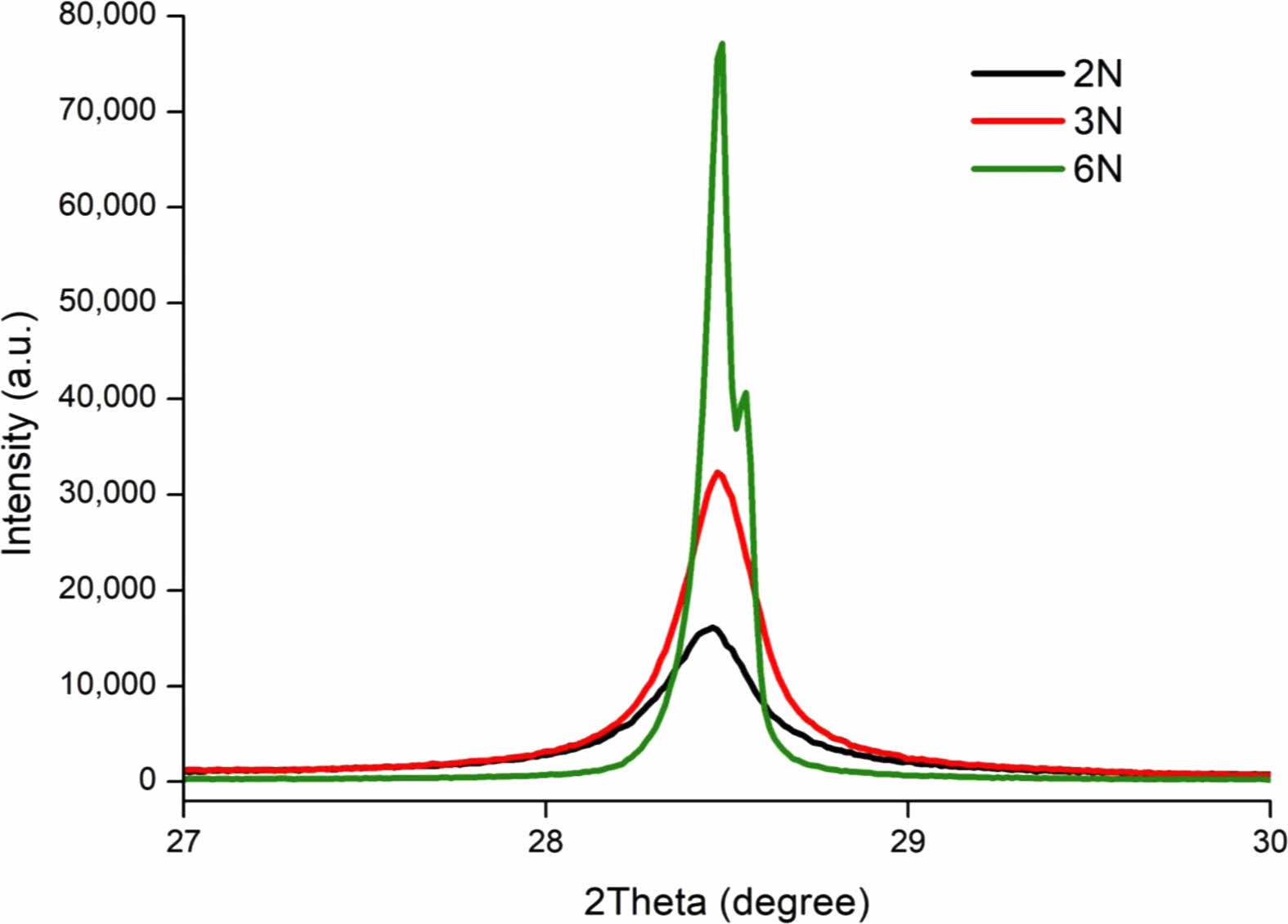
Higher Si crystallinity has higher Li ion storage capacity and has lower number of impurities to reduce the number of irreversible reactions in battery cell. Fig. 1. Is the XRD spectrograph results to identify the crystallinity levels in relation to purity. 99% (2N) Silicon Nano Particles (SiNP) display the lowest XRD peak intensity while 99.9999% (6N) shows the highest peak intensity. The higher peaks indicate higher crystallinity levels. Mono SiNP and Poly SiNP were used for their high initial crystallinity levels to obtain Si with high crystallinity. The first milling process was done with the gyromixer milling and the second milling process was done with planetary milling. XRD was used to observe the effects of milling on crystallinity Fig. 2, increasing crystallinity leads to high capacity and cycle efficiency properties [58-60].
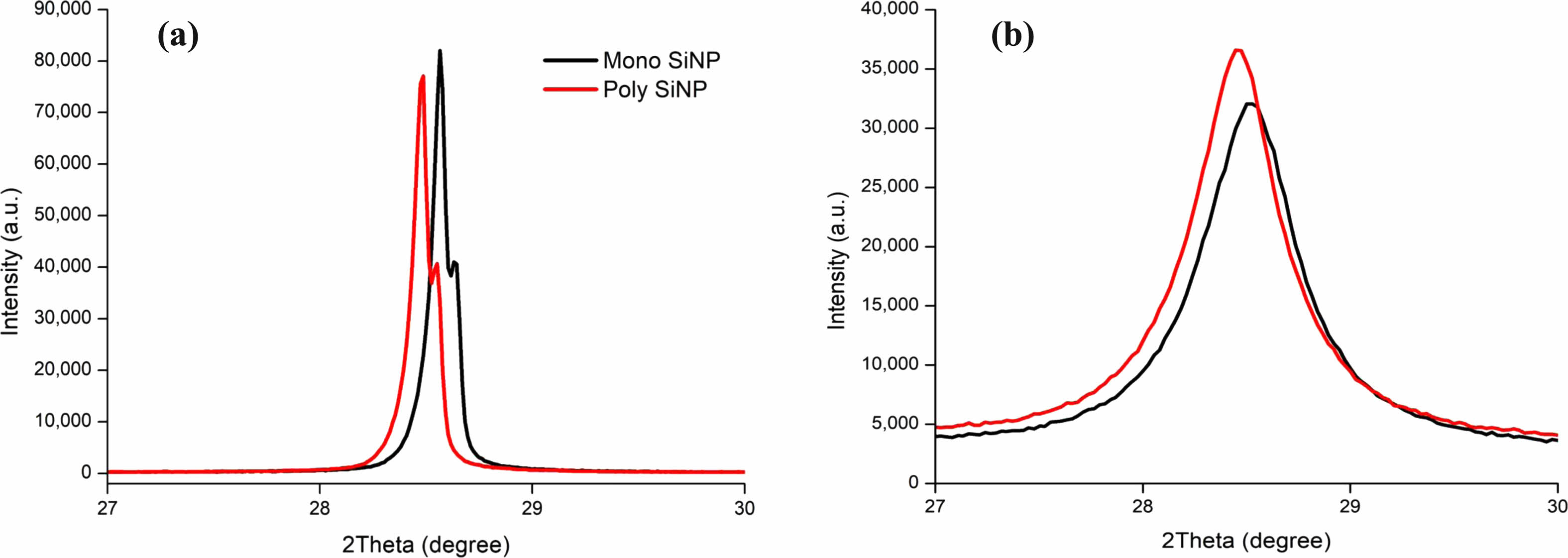
The result of the first milling process showed the XRD peak having near identical levels of height, but Mono silicon resulted in a 7% higher peak. Full width half maximum (FWHM) values indicate Mono SiNP has a value of 0.103, and Poly SiNP has a value of 0.104 resulting a slightly less crystallinity level for Poly SiNP Fig. 2a. This result coincides with Shabir and Pokale’s research where they identified Mono Si has higher crystallinity levels to Poly Si by XRD peak’s intensity and the line’s smoothness. The first milling process showed us that samples with low crystallinity levels are affected more by the ball milling process. The pulverized particles were placed into planetary milling with higher RPM and smaller Zirconia Oxide (ZrO2) balls for further miniaturizing Fig. 2b. The 12 hours of high RPM milling damaged the high crystallinity properties and Mono SiNP that had higher crystallinity levels was more affected by the process. The resulting FWHM values for Mono SiNP and Poly SiNP are 0.552 and 0.535, respectively.
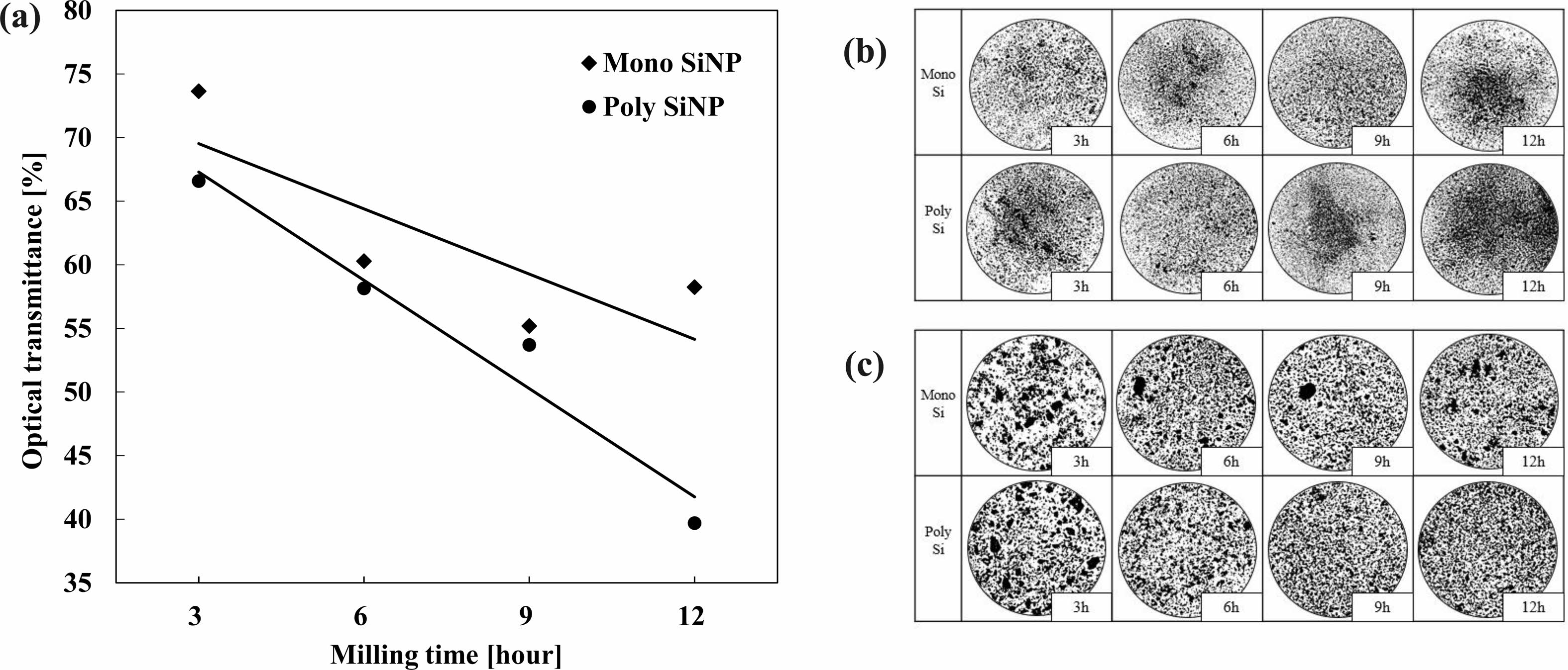
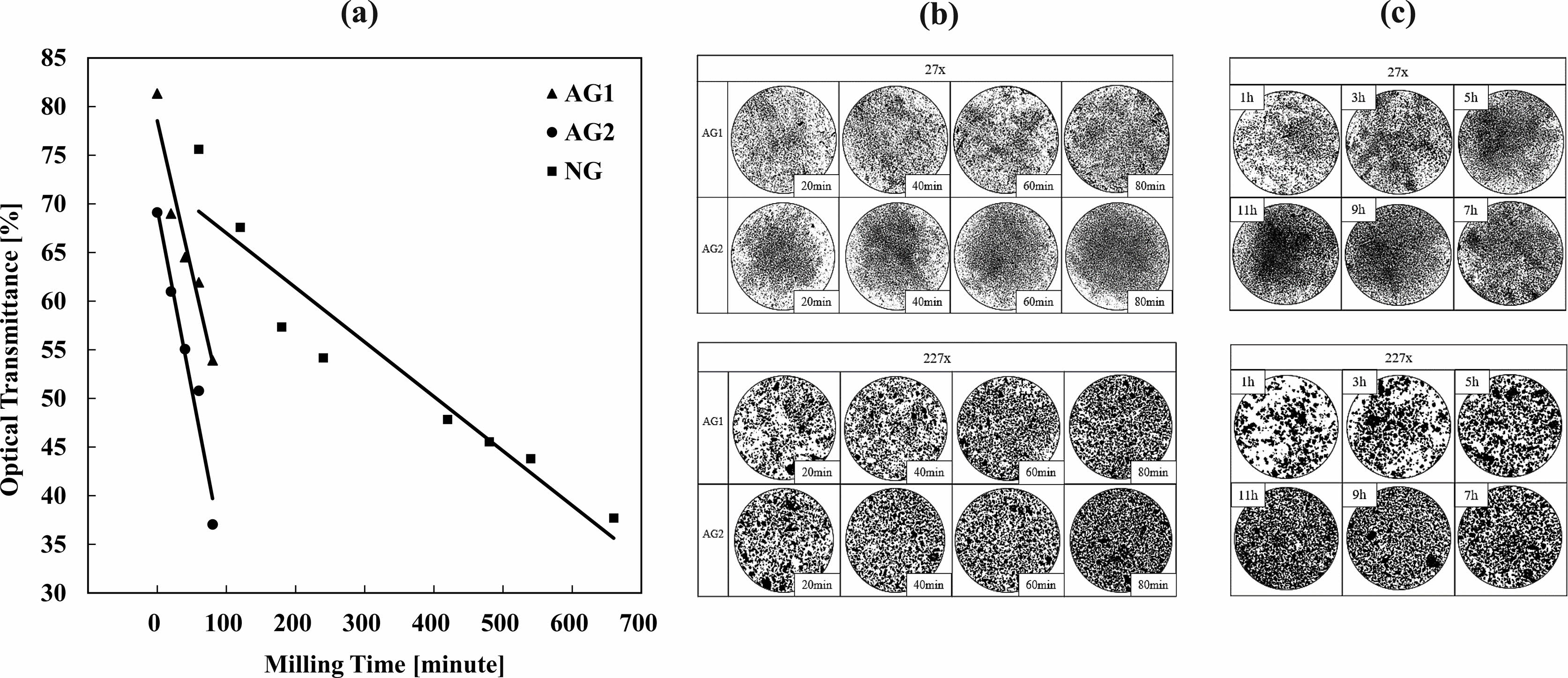
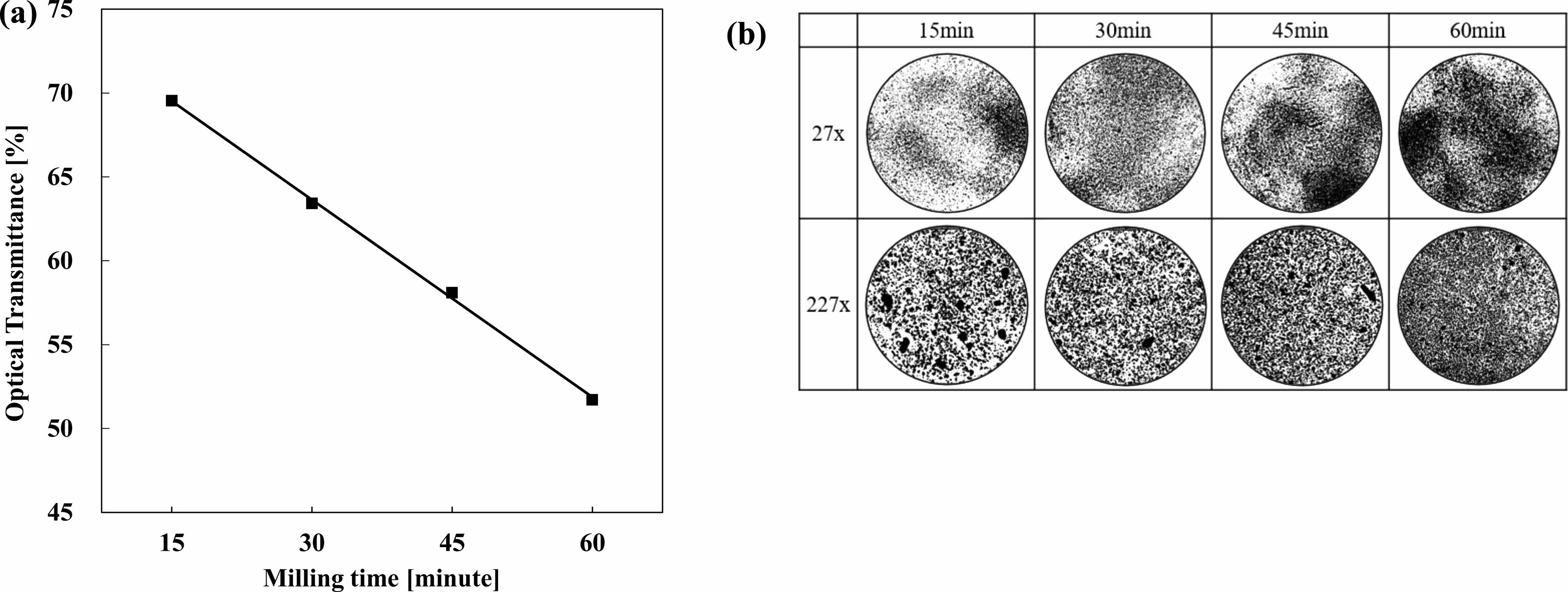
Fig. 3a, we observed the change of the particle sizes via optical transmittance rates. We observed the transmittance rates through the particle’s increasing surface area though miniaturization blocking the light source given the same weight [61, 62]. Mono SiNP and Poly SiNP have the optical transmittance rate difference of 5% after 3 hours of milling and 12% after 12 hours of milling, difference increasing coming from milling time increasing. Fig. 3b, the picture of the particle distribution with an optical microscope, magnification (27x) shows Poly SiNP has darker contrast than Mono SiNP. Magnification (227x) shows Poly SiNP had uniform distribution of particles while Mono SiNP has occasional clustered or congealed particles. Under the same milling conditions, Poly SiNP with slightly lower crystallinity has more pulverization, and confirms crystallinity affects the particle sizes.
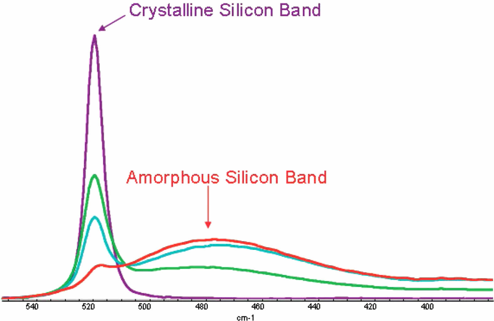
Deschaines and Hodkiewicz’s research on using Raman spectrograph to research Si gives a clear example of the difference between the crystalline Si bands and Amorphous Si bands Fig. 4 [63]. Silicon created with CVD methods are an example of low crystallinity. Laser driven chemical vapor pyrolysis is used to improve crystallinity from amorphous to polycrystalline for higher electrical capacity [32].
Heat treatment has two different stages of effect onto the material Fig. 5. The first stage is when the XRD peak’s intensity increases from the removal of impure materials and the second stage is when the high temperature begins to anneal Si and potentially form different crystalline as suggested by Merchri and Chihi [64]. Heating experiments are conducted in vacuum which excludes the possibility to add other impure substances, for example oxygen, though the heating process [65].
Crystallinity of Graphite Particles
Graphite is composed of layers of carbon atoms that are arranged in six sided hexagonal rings. These rings are attached to other rings on their edges and form infinite patterns. The higher the crystallinity of graphite, the higher amounts of layered structures develop. Leading to feasible formation of stable carbon lithium electron pair bonds. Higher crystallinity means higher amount of lithium ions inserted between the carbon layers results in a higher discharge capacity [66, 67]. Graphite crystallinity in the experimentation progress greatly affects electrical capacity, similarly the crystallinity of SiNP affects the capacity of the battery. Welham and Berbenni show that the longer the milling time, the Raman graph’s 1D peak intensity grows, it indicates the presence of amorphous graphite [68]. Emphasizing the milling time in which needs to be taken careful consideration due to the sharp reduction in graphite crystallinity when extended milling time [69, 70].
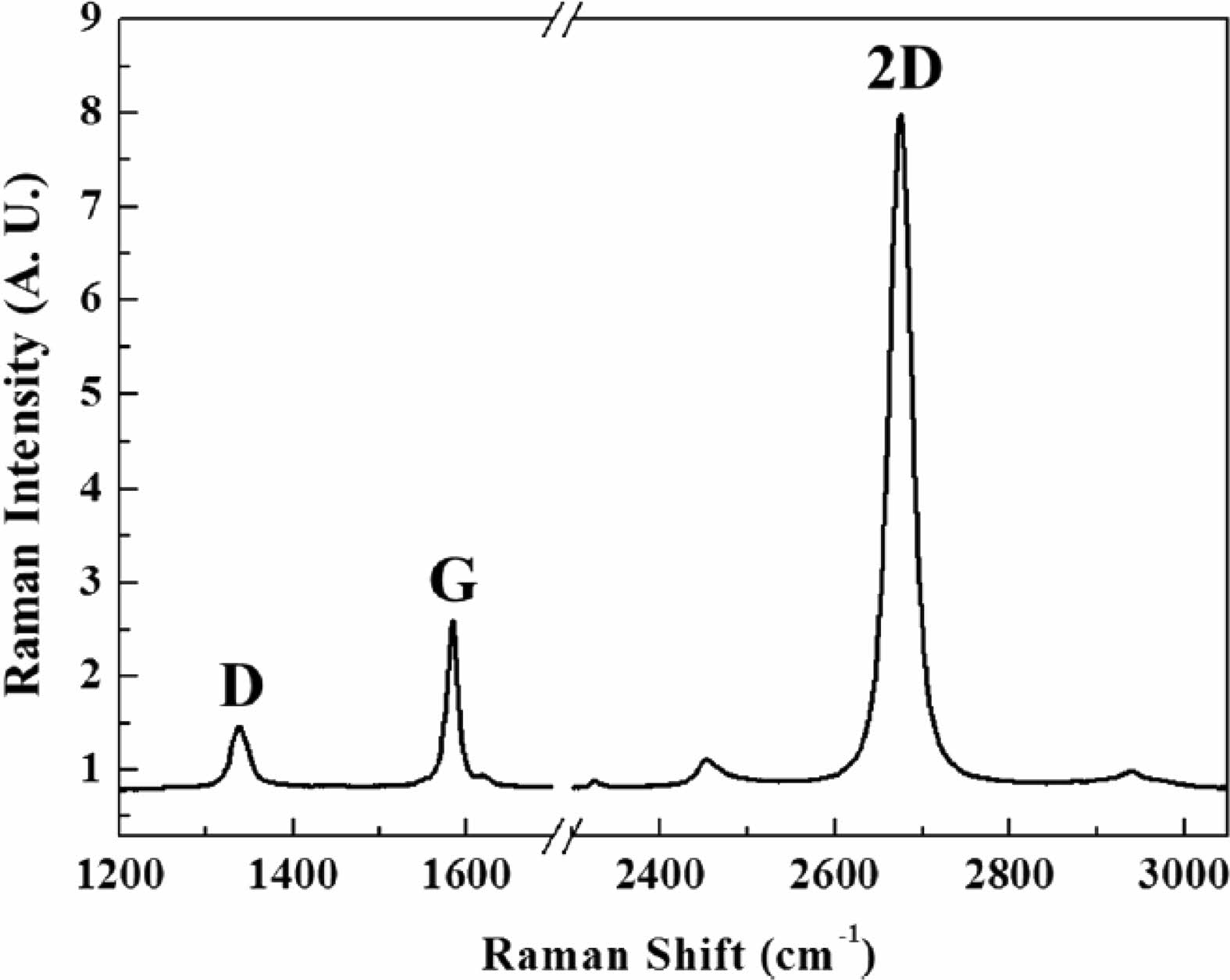
The presence of conductive graphene scaffolding greatly enhanced the kinetics of charge transfer presented by Wenyu Zhang and Yi Zeng [71] giving reason for the advantages of milling and providing a graphene shell. Graphene nanosheets provided similar improvement the conductive network suggested by Li Wang and Haibo Wang [72, 73]. Where the graphene layer greatly reduces interfacial diffusion and for the formation of silicide [74]. For this reason, we conducted experimentations in graphite milling time periods and examined their XRD and Raman peaks. The ratio between the 1G and 2D peaks will suggest the potential formation of graphene through the process. Confirming this to be true will assist in the integrity of the silicon shell as shown by the difference in Raman spectrum provided by Yufeng Tang as the absence in graphene resulted in the peak heights of the XRD lower than the results with graphene [75].
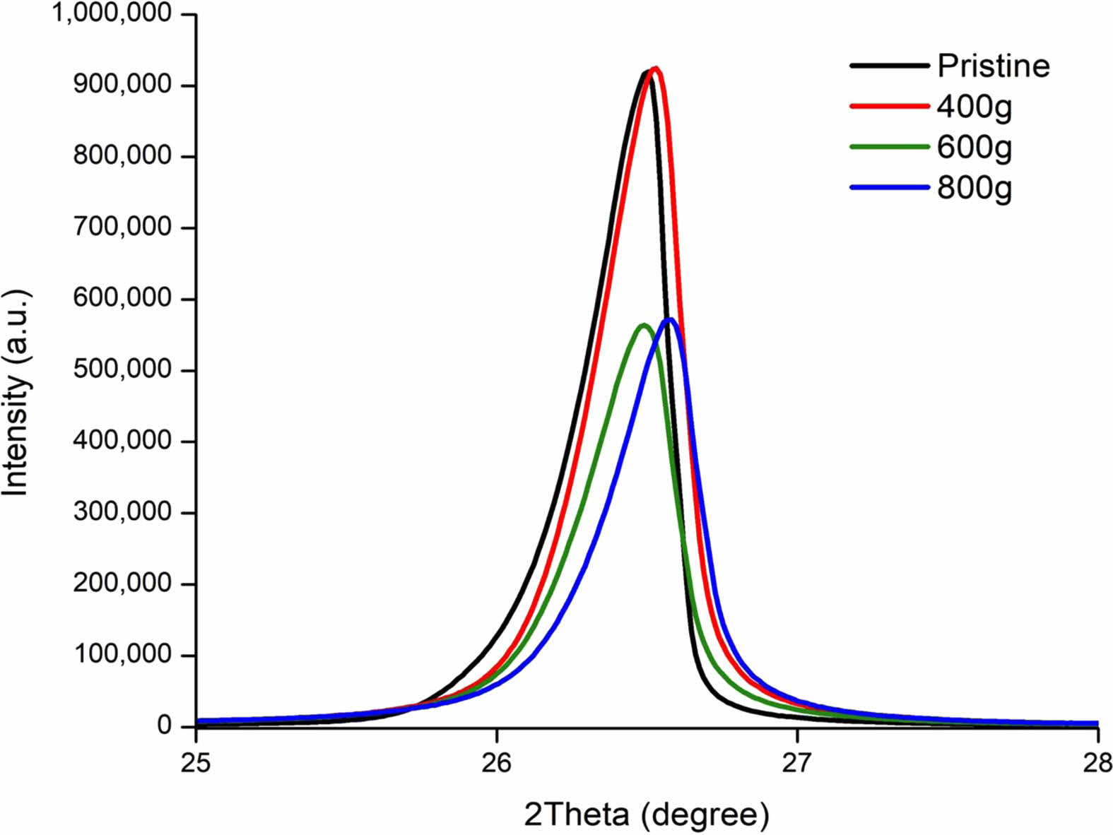
400 g of Zirconia balls was placed with 5 g of Natural Graphite (NG). After 100 minutes of milling, the congealed particles that could be seen prior to milling were crushed and dissipated into smaller particles. The miniaturization of particles became more apparent when the amount of the balls increased to 600 g and 800 g respectively seen on Fig. 6. 400g of Zirconia balls minorly increased the crystallinity peak. Park and Lee’s research suggests this miniaturization will contribute to the increase of cycle life and initial charge capacity (ICE) [76]. However, increasing the Zirconia ball load to 600 grams resulted in a sharp 39% decrease of the crystallinity peak. This concluded that the crystallinity of NG can stably withstand certain levels of pressure but the structure collapses once the threshold has been exceeded. In all cases, NG crystal structure is proven to be more robust and gave the possibility to be a sufficiently protective material to keep the carbon shell intact during lithiation [77-80].
The optical transmittance rate of NG, Artificial Graphite (AG1) and AG2 by milling time are shown on Fig. 7a. When AG1 and AG2 were milled for 80 minutes, the optical transmittance rate decreased by 15% and 22% in comparison to 20 minutes of milling time. AG2 showed more significant change than AG1 when milled in identical conditions, indicating it is more appropriate in making smaller particles in shorter time. Comparison between NG and AG shows the optical transmittance rate decreased by 10%, AG2 requires 40 minutes of milling time while NG requires 180 minutes of milling time. AG2 has lower crystallinity values than NG and needs shorter milling time for the optical transmittance rate to drop by 1%. This gives us insight into the effect of crystallinity on the optical transmittance rate and how high crystallinity requires longer milling time for the particle sizes to decrease.
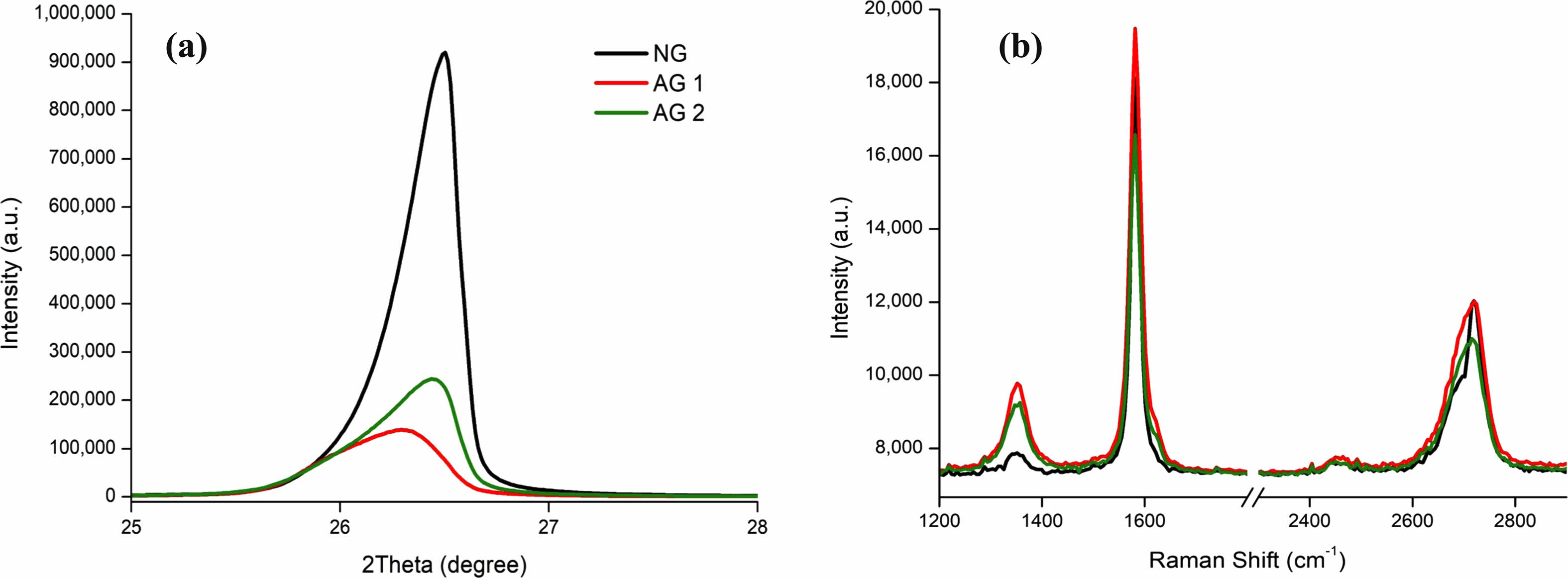
Three samples of NG, AG1, and AG2 were observed in their pristine state with both XRD and Raman spectra. NG shows the highest crystallinity with the XRD spectrum Fig. 8a that supports the results from Fig. 7. The relationship between 1D, 1G, and 2D peaks were calculated to identify the average number of potential graphene layers. The results were similar across the board with a 2D/G ratio of 0.66. Resulting in several the potential of several unorderly graphene layers Fig. 8b. The Raman spectra confirmed by having a low 1D peak in comparison to AG1 and AG2, indicating the amount of amorphous carbon is low [81] while exhibiting a high 1G peak height similar to other graphite samples. This leads back to the XRD spectrum where the higher crystallinity implies the presence of graphene.
The XRD spectrum of AG1 and AG2 when milled for 0, 40, 60, and 80 minutes are shown on Fig. 9b and Fig. 9d. Both AG1 and AG2’s XRD spectrum, intensity greatly increases as it is milled showing large contrast to the steady decrease in transmittance rates Fig. 7a. The decrease in transmittance rates can also be confirmed by Fig. 7b and 7c where the amount of white space decreases with the increase of milling time. The results from Fig. 7 indicate the particle sizes are not necessarily related to the XRD spectrum and the crystallinity levels.
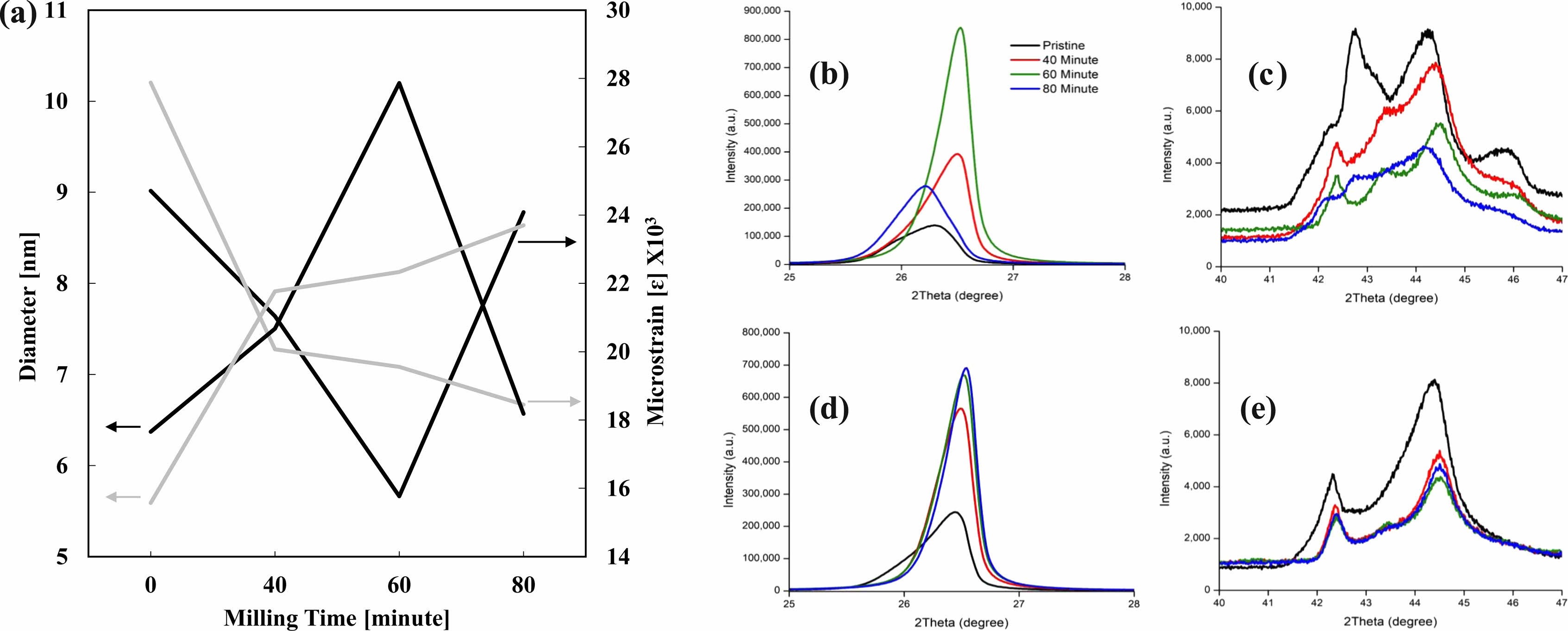
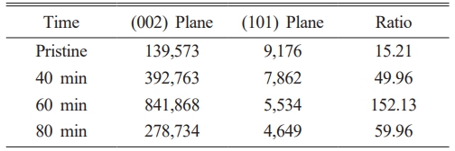
The detail was observed by calculating the internal strain value of each crystallite to identify the cause Fig. 9a. The XRD spectrum’s behavior is attributed to the energy and heat created by the milling process that puts energy onto the crystals, increasing its crystallinity and decreasing the FWHM value of the XRD spectrum. A similar example is mentioned in Zhang and Zhifu’s research with the FWHM value of Mo decreasing and increasing according to different milling times [82]. It’s noticeable how the XRD peak increases until the 60-minute mark and shows a sharp decline at 80 minutes from the collapse of its crystal structure. The energy put towards the crystal collapses the crystal structure from too much energy. When the crystallite’s size reaches critical at the 60-minute mark, it collapses with the XRD spectrum showing a significant drop as well Fig. 9b. The detailed values of the XRD peaks are given in Table 1.
Natural Graphite particle size (D50) decreased from 20 um to 5 um Fig. 10. However, no change in Raman Spectra indicating there was no effect of milling to its crystallinity. AG1 particle size (D50) decreased from 20 um to 8 um. AG2 particle size (D50) decreased from 12 um to 2 um. AG1 and AG2 displayed a decrease in the 1G peak’s intensity Fig. 10a & Fig. 10b. This indicates the decrease in crystallinity levels. AG1 showed no change in 1D peak’s intensity whereas AG2 showed a visible decrease in 1D peak, it allows us to conclude AG2 potentially formed graphene during milling process as the 1D peak represents the amorphous.
We took Raman spectra samples from NG, AG1, and AG2 Fig. 10 and compared them with the mono layer graphene sample Fig. 11 [83]. We applied the four different categories of determining the formation of graphene suggested by Jung and Jeong [84] assuming the provided sample has graphene. The 2D peak location, the ID/IG ratio, the I2D/IG ratio, and the intensity levels of XRD peaks are the four factors observed to determine the presence of graphene on second milled samples. The 2D peak for the mono layer graphene is 2680 cm-1. The milled result of NG, AG1, and AG2 are close to this result respectively. The ratio between ID/IG ratio which indicates the number of defects in the graphite sample lands on 0.491, 0.593, and 0.454 which is close to the mono layer’s ratio of 0.576 indicating a low number of potential defects. This ratio has close relations to the potential capacity of the anode, with lower values having better capacity [85]. The increase in this ratio causes decrease in the structural stability of the graphite as experimented by Murugaesan and Gopal with 6-hour milling having the harness of 77.4 but 12-hour milling having the hardness of 46.2 [86].
The I2D/IG ratio indicates the potential layers of graphene. The values of 0.676, 0.715, and 0.653 are indicators of multiple layers of graphene. The higher this number is, the more likelihood of the sample having fewer layers of graphene.
As the ball milling time increases, the intensity levels of the diffraction peaks decrease at 2θ=44.4°, 50.6°, and 59.8°, corresponding to (101), (102), and (003) planes, while the peaks increase at 2θ=26.3° and 54.6°, assigned to (002) and (004) planes of graphite (JCPDS card No. 75-1621). This is due to sliding between the graphene layers in graphite in an in-plane direction due to the ball milling.
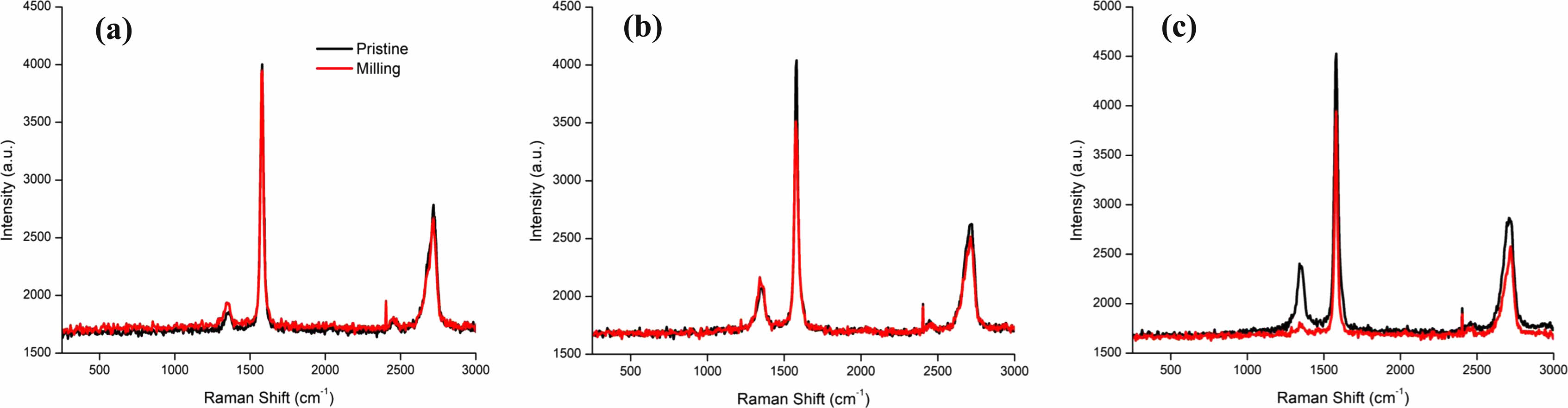
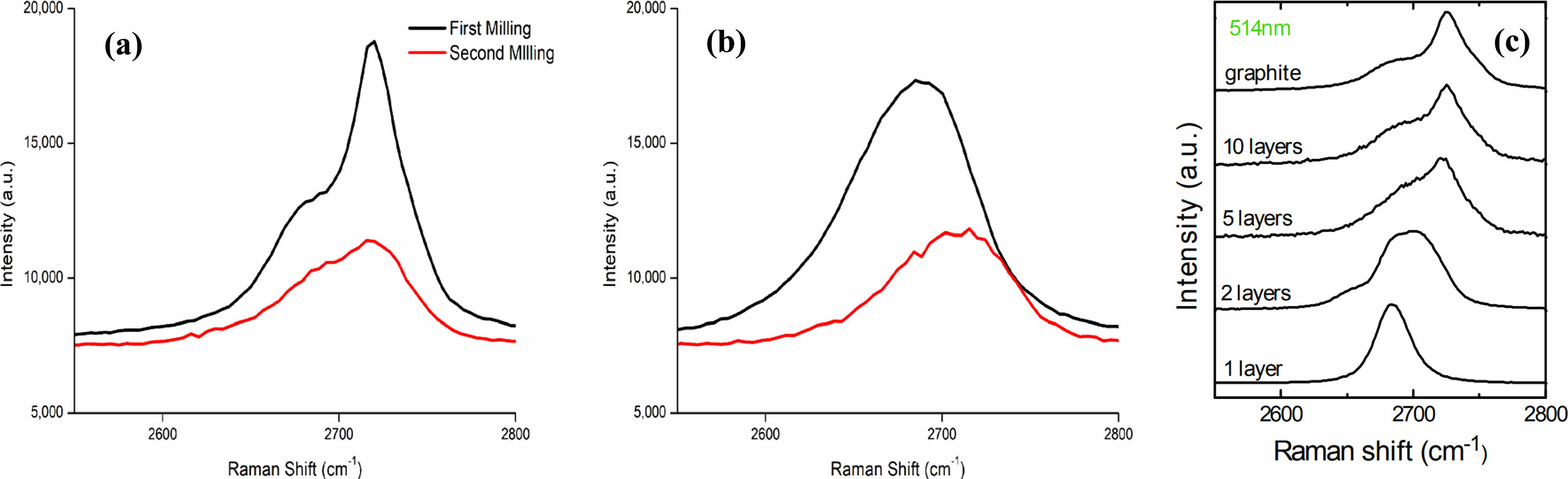
The Raman spectrograph of the 2D peaks of Natural and Artificial Graphite samples that were milled for 12 h are shown on Fig. 12a, Natural Graphite (NG) showed a peak shift from 2719 cm-1 to 2715 cm-1. Fig. 12b, Artificial Graphite (AG) showed a peak shift from 2684 cm-1 to 2701 cm-1. The 2D-band at 2660-2680 cm−1, assigned to the second order of the D-band, shifts due to ball milling for 72 hr. The shift in the peak of the 2D band is attributed to the thickness of the ordered graphite. This can be cross examined with Fig. 12c, from Ferrari and Basko’s research. Indicating the 2D peak location of milled graphite is in close location to the known location of graphene formation [87]. The evidence above can suggest the planetary milling process resulted in the formation of graphene from milling graphite. Among these three samples, AG2 showed the most promising potential of forming graphene.
The confirmation of the presence of graphene is an important detail since graphene is used as an additive to improve charging speeds of Li ion batteries. While the previously emphasized limitation of graphene is their preparation methods and cost [88], we were able to solve this aspect by confirming the formation during the milling process. Eliminating the concern of cost and process as there is no requirement to separate pure graphene.
Crystallinity of Carbon Particles
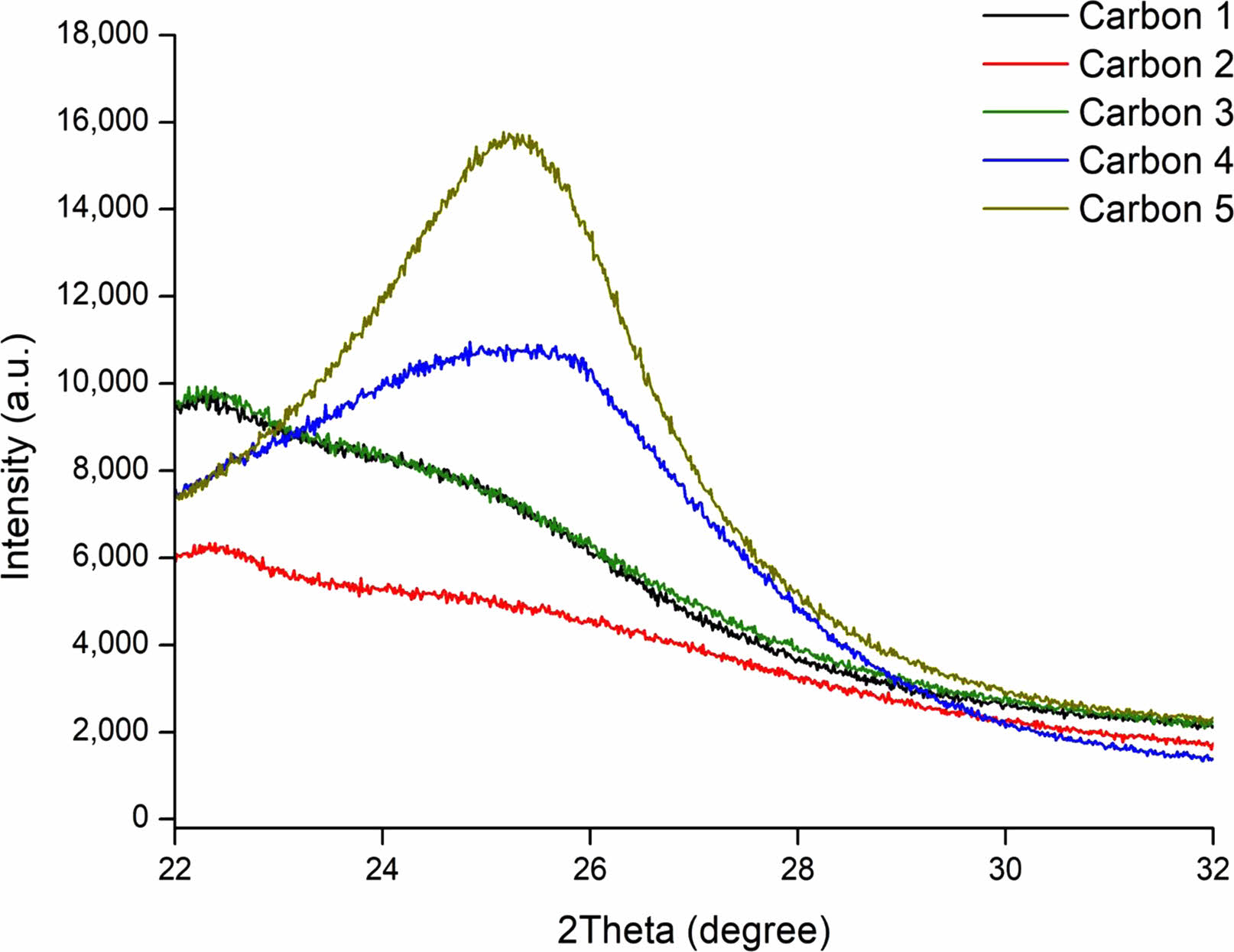
Some examples of coating amorphous carbon into crystalline silicon forming robust carbon shell showed high-capacity results [89]. With the protective carbon shell preventing the Si core from getting in touch with electrolytes around it. Graphite or coated carbon layers in large quantities accommodate the volume change and prevents the quick loss of capacity as well as extending the cycle stability [90-93]. Carbon nano fiber, nano Si with nano fiber composite, and carbon nano tubes exhibit a high initial capacity because of its porous web like structure as well as strong encapsulation of the silicon particles provides ample room to volume changes and provide cyclability [94-99]. This structure is coated with a unique carbon material Lemon Energy devised named NanoMollisAdamasTM (NMA) that will form the robust protective shell.
Our NMA sample shows the highest carbon peak in Fig. 13 with the label of Carbon 5. This shows its superior crystallinity against other reference materials shown in comparative XRD spectrum. Extracted amorphous carbon has its max peak between 22θ and 23θ as shown by Rajan and Sampath’s research [100]. This coincides with the example with glassy carbon A and M indicating that A and M are amorphous examples. Carbon 4 and Carbon 5 on the other hand are from CVD methods. The results of these procedures placed the two samples onto 24 theta which is the XRD spectrum for crystallite carbon. We have established previously in the paper that higher XRD peak results in higher purity samples though crystallinity. Electrical capacity, initial coulombic efficiency, and rate performance will improve due to the higher crystallinity of NMA carbon shell. Pitch carbon is commonly used as carbon material in graphite and silicon anode materials. Carbon 3 in Fig. 13, XRD spectrum of pitch carbon, which shows low crystallinity levels due to its amorphous nature. Pitch carbon is made from various sources such as coal or petrol tar and has properties close to soft carbon [101]. While also providing the benefits of elasticity and acting as a bonding agent [102].
Hard carbon with high temperature treatment is capable of greatly extending its capacity retention rate for up to 79% for 700 cycles, commonly used in capacitor applications [103-105]. The XRD spectrum as seen on Zhu and Gu’s research shows sharp XRD peaks that show similar carbon formation to Carbon 1 through 4 [106]. This comparison signifies the significantly higher crystallinity levels of the NMA sample coating which leads to higher hardness levels of the carbon shell. Particle size can also affect electrical conductivity as experimented by Pramono and Rahman, as their experiment addresses the ratio of carbon within a composite. In composites with low percentage of carbon composition, smaller particle sizes showed an increase of conductivity [107].
Soft carbon shows contrast to hard carbon for lower potential capacity but higher cycling rates due to lack of crystallinity [108]. However, higher temperatures shift its properties closer to commercial graphite [109-110]. Soft carbon made from pitch at high softening temperatures displays an increase in its crystallinity levels thus increasing its initial capacity and rate performance. The experimentation results show heat treated soft carbon at high and low temperatures. This displays low irreversible reactions but low capacity if it was treated at high temperatures. In contrast low temperature heat treatment results in high initial capacity but low cyclability due to irreversible reactions [111]. There were contrasting results where the higher heat treatment temperature has the effect of decreasing the potential capacity with Boron doped carbon [112].
Carbon Nanotubes (CNT) are unique in their structural strength combining multiple advantages such as tensile strength and high rigidity. Though these relative traits over graphite, it can demonstrate higher potential capacity in comparison to commercial graphite anode materials as seen in Jin and Sun’s research. The inclusion of 5 wt% and 10 wt% CNT into LiFePO4 displayed a steady cycling performance in higher C rates [113, 114]. The example the CNT provided by Ngoma and Mathaba shows that it has high XRD peaks [115]. It can be utilized as an additive material to increase the robustness and higher electrical conductivity for all cases of silicon anode material structures [116-119].
Graphene has a web like composition that can consist of single to multiple layers. The fewer layers give graphene has more flexible and robust structure. The creation process results in high crystallinity leading to high potential electric conductivity. Like CNTs, it can be utilized as additive materials to increase the robustness of Si anode material structures [120].
Crystallinity of Silicon/Carbon Composite Particles
Silicon and graphite were milled together to observe the effects of milling towards compounds. The results from milling experiments were tested with light transmittance rates and XRD spectrum. Overall, longer milling times show the decrease of particle sizes as seen in Fig. 14. This can be compared with Fig. 7 where it held only graphite. The decrease of transmittance rate is similar as it decreased by 20 over 60 minutes, which indicates that the rate is not affected by the presence of silicon particles.
In contrast, the inclusion of SiNP into graphite milling greatly affected the XRD spectrum as shown in Fig. 15b. In comparison to Fig. 9b, the relative height of the peaks greatly diminished to less than 1%. This is because the harder silicon particles collide into the graphite particles during milling process, causing more direct energy onto the graphite particles even in short milling times [121-123].
In contrast to the sharp fall of the graphite XRD peaks, SiNP peaks increased the longer it was milled. This can be attributed to the sealed environment and the High Energy Ball Milling (HEBM) removing the impurities from the surface of the SiNP. This result is in contrast to the result from Parajina and Pascal’s or Patino and Tellez’s research. However, this research utilized chrome steel as the bowl and stearic acid or cyclohexane as mediums and longer milling time while our research was done within sealed normal atmosphere in shorter duration [124].
Chemical Vapor Deposition (CVD) method was used to pyrolyze methane (CH4) gas into carbon and hydrogen. CH4 being a reliable carbon source supporting 33% of carbon contents. This method provides stability and high conductivity through a uniform distribution of materials and provides the ability to fine tune the input rate, temperature, and the thickness of the applied material [125-127].
The amount of C coated onto Si is affected by multiple factors. Temperature is a major factor from the pyrolysis rate of methane gas as it exponentially increases with temperature [128-130]. Internal pressure of the chamber is also a key factor as the pyrolysis rate of methane steeply drops at high pressure. The Back Pressure Regulator (BPR) assists in making sure the internal pressure of the chamber does not hinder the pyrolysis rate.
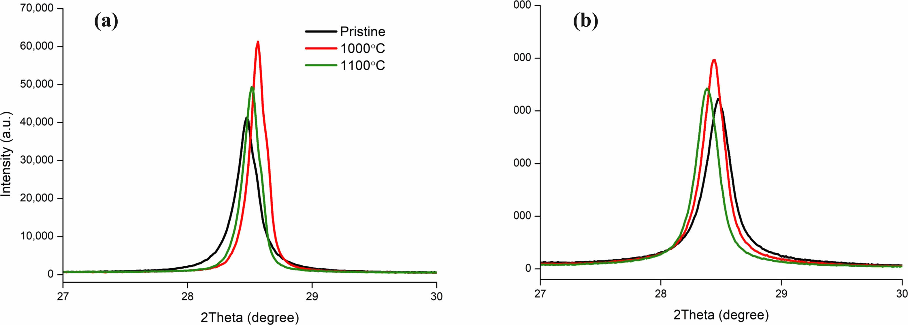
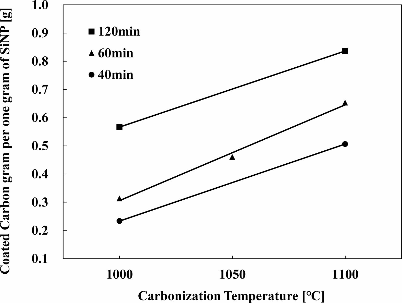
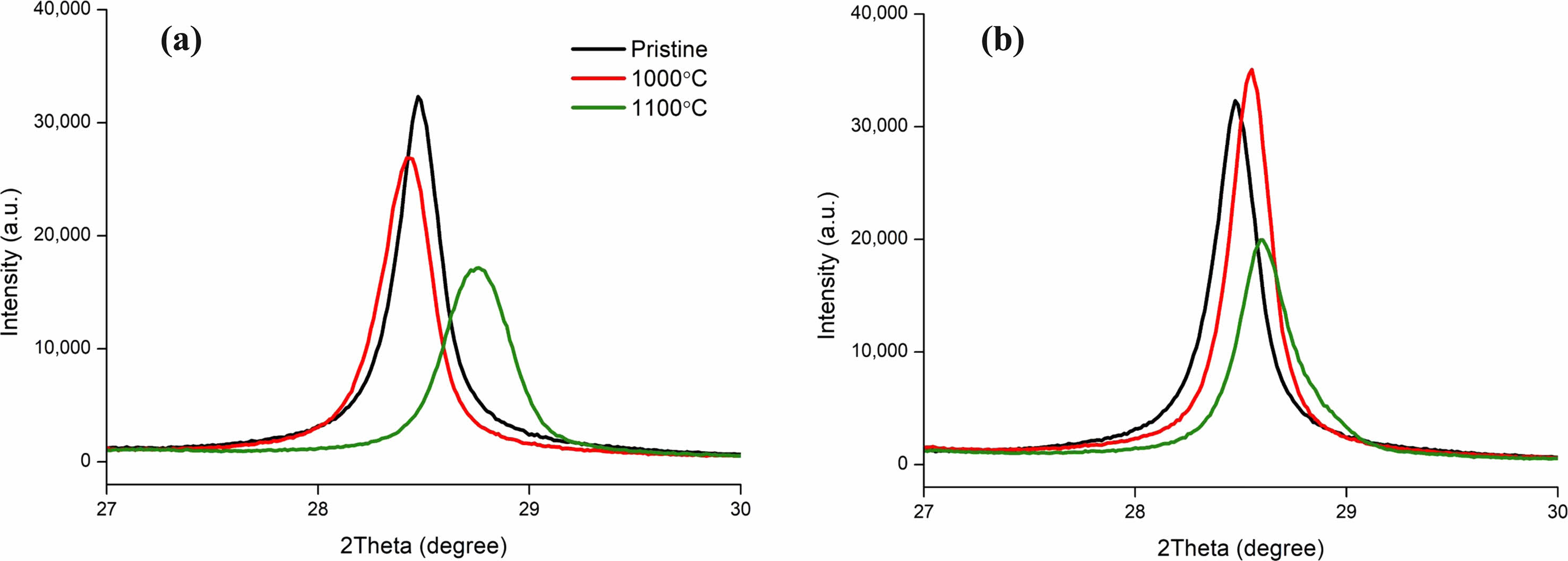
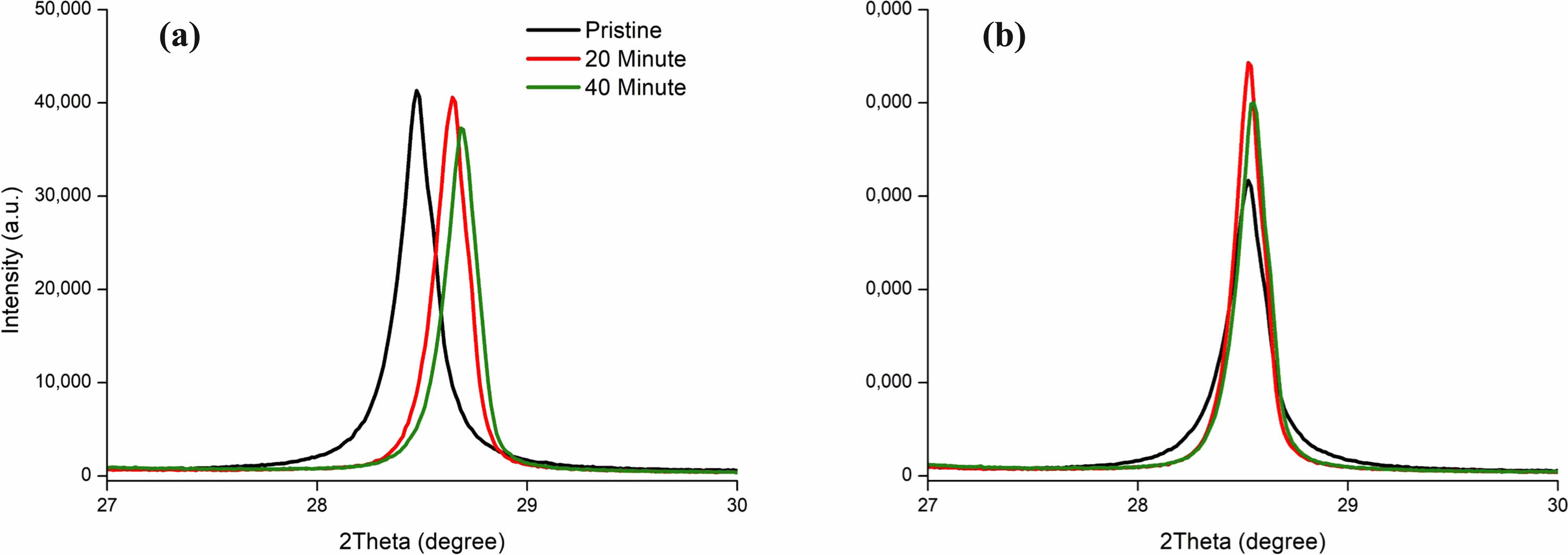
The temperature of the tube furnace was increased to 1000 ℃, 1050 ℃, and 1100 ℃ to test the effects of temperature. Methane gas was injected into the quartz tube at a pressure of 0.5 SLPM (Standard Liter Per Minute) for 40, 60, 120 minutes to test the effects of temperature Fig. 16 [131-133]. The result of the above process is a nanostructure encapsuling silicone with carbon [94]. The thickness of the coating was measured by grams of carbon per 1 gram of silicon particles. 1100 ℃ showed the thickest carbon layer in a set amount of time. Comparable results are presented in the paper written by Son and Park as it displays how time and temperature affects the carbon coating. Pristine Si has been exposed to H2 and CH4 at a temperature of 1000 ℃ and 1100 ℃. The difference can be seen in the XRD spectrum that for 1000 ℃, while the SiOx peak predominately shows itself, the carbon peak is not visibly present. The XRD spectrum provided for 1100 ℃ displays the increasing XRD peak of carbon between 10 and 30 minutes [134].
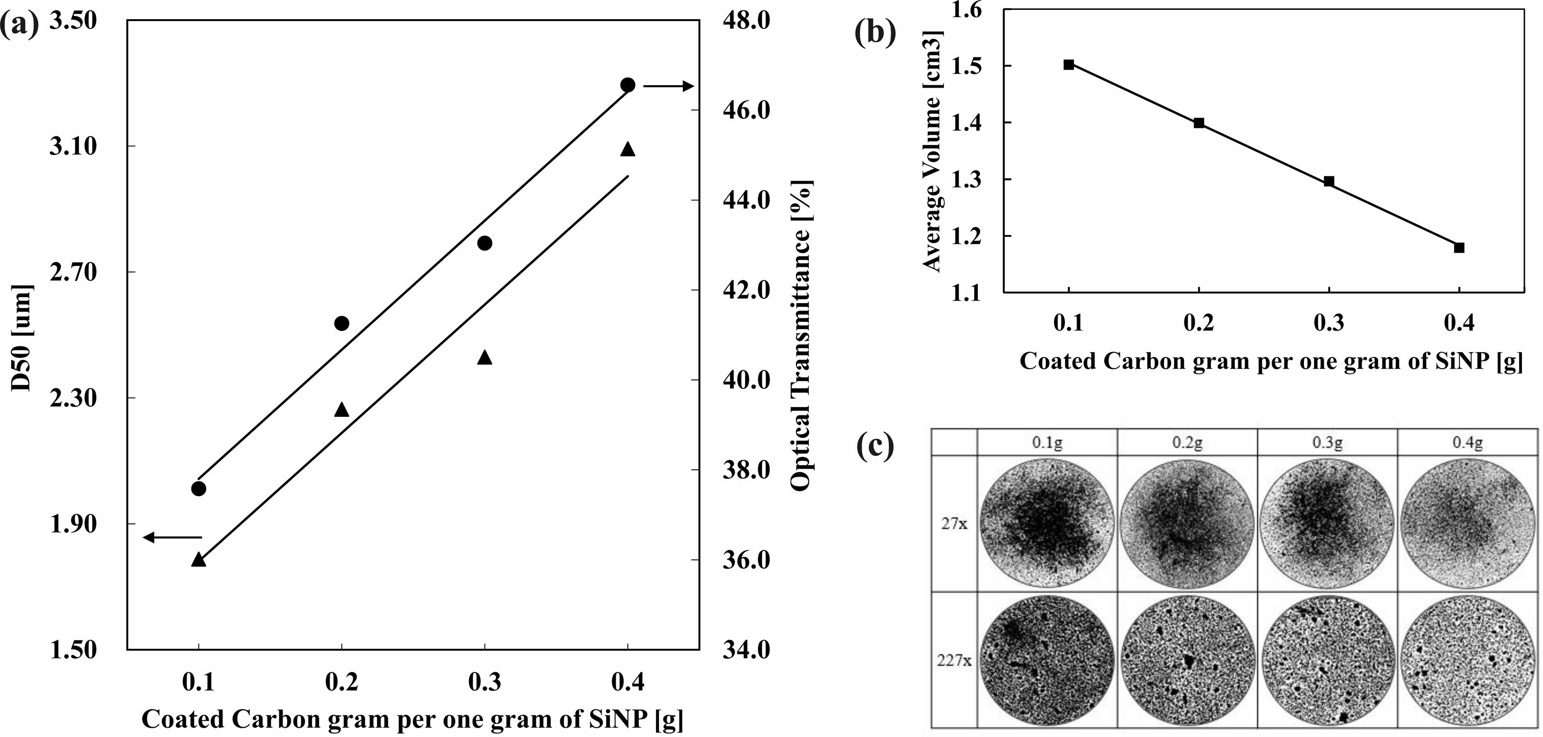
The correlation between the amount of carbon coating with particle’s D50 size can be observed on Fig. 17. The increase of carbon coating amount on to Si particles results in the increase of D50 sizes and transmittance rates. This graph can relate to Fig. 16 to see the increased amount of carbon coated per gram is proportional to the time coated. The steep increase of transmittance rate from 0.3 g to 0.4 g implies the increase of particle size and the thickness increase of the carbon shell is much faster with the increase of temperature.
High temperature during processing leads to an increase in the SiNP’s XRD patterns [135-139]. While the example given was for silicon nanosheets, this can be proven the same for SiNP with XRD graphs of our experiments Fig. 18. This result suggested that a temperature range between 1000 ℃ and 1100 ℃ was ideal for our experiments as 1000 ℃ showed higher crystallinity than 1100 ℃ thus a higher chance to be a more suitable solution in protecting the core shell. Mikito and Humihiko research also shows Si’s XRD intensity increasing when annealed at high temperatures.
The shifts in the XRD spectrum of the milled silicon material in Fig. 19 can be attributed to the defects introduced during planetary milling. According to the research of Takashi Sawabe and Masafumi Akiyoshi, the higher temperatures of heat treatment could recover the shifts to their original locations [140]. However, we observed shifts in the XRD spectrum peak after carbon coating. We added graphite into the silicon mix before milling because graphite reduces surface friction [141-143]. The addition of graphite to SiNP reduced the shift of the XRD spectrum as seen in Fig. 19b. The SiNP that included graphite shifted much less than the SiNP that did not include graphite. Giving us the insight that the addition of graphite protects the integrity of the SiNP.
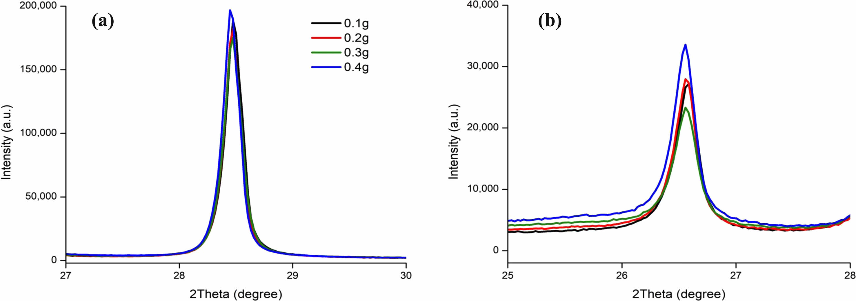
Silicon and graphite peaks showed no meaningful change in the XRD spectrum peak with the increase of the thickness of the carbon coating Fig. 20. This would indicate that the amorphous carbon added to SiNP does not impact crystallinity.
The Raman spectra result of the carbon coated sample SiNP (99%) is shown in Fig. 21b. The first peak at 520 cm-1 represents Si, the 1D peak at 1351 cm-1 represents the presence of amorphous carbon layer made from CH4 gas. The presence of the relatively lower 1G peak supports the higher ratio of amorphous carbon like the example of faulty graphene samples.
However, the 2D peak that can be seen in Fig. 21 is different to Raman spectra examples where it displays graphite with complete absence of graphene and the shown Raman spectra peaks are much lower in comparison [144]. It has been established there is a high chance of graphene forming through the milling process, the 2D peak represents the presence of graphene even after the carbon coating process [145].
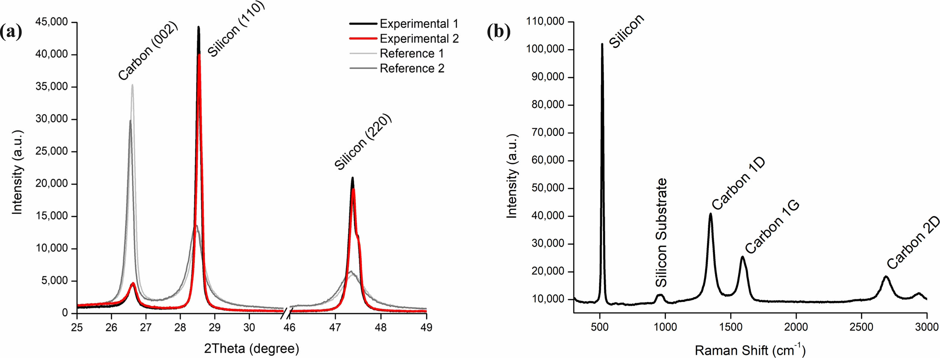
The comparisons among silicon carbon composite anode materials, Lemon Energy’s experimental products 1, 2 and market products 3, 4 are shown in Fig. 21a. The significantly higher silicon peaks, experimental 1&2, represent high purity SiNP has good crystallinity. Fig. 21b represents the Raman Spectra of Experimental 1 sample. G peak means sp2 bonding of graphite, and D peak is related to disordered structure such as diamond-like or amorphous carbon, so the degree of structural disorder can be quantified as ID/IG ratio [146]. Experimental 1 has an ID/IG of 1.61, indicating that very amorphous carbon is coated on silicon. The relative height of the 1G and 2D peak suggests that the graphene formation prior to the carbon coating process, which is diminished in intensity due to amorphous layer. However, the presence of the 2D peak signifies the existence of graphene, which will be expected to improve the robustness of anode materials and its electrochemical performance.
|
Fig. 1 XRD Spectrum of Silicon (111) by Silicon Nano Particles (SiNP) purity |
|
Fig. 2 XRD Spectrum of Silicon (111) by Silicon Nano Particles (SiNP) by crystallite types. (a) Drying milling for 12 hours with Gyro Mixer, 100RPM, 10 mm Zirconia balls, (b) Wet milling for additional 5 hours with Planetary Mixer, 300 RPM revolution+690 RPM rotation, 0.6 mm Zirconia balls. |
|
Fig. 3 Mono Silicon (Mono SiNP) and Poly Silicon (Poly SiNP) comparison by Milling time (a) Optical Transmittance, Optical Microscope (b) 27x, (c) 227x. |
|
Fig. 4 Raman Spectra of silicon samples ranging from pure crystalline to one containing predominantly amorphous silicon. [63] |
|
Fig. 5 XRD Spectrum of Silicon (111) Silicon Nano Particles (SiNP) by Heat Treatment and Carbon Coating Temperature at 1000 ℃ and 1100 ℃, (a) 99% Purity SiNP Heat Treated for 1 hour, (b) 99.9% Purity SiNP Heat Treated for 1 hour. |
|
Fig. 6 XRD Spectrum of Graphite (002) plane, Natural Graphite (NG) for 100 minutes milling by the Zirconia Balls weight. |
|
Fig. 7 Artificial Graphite 1 (AG1), Artificial Graphite 2 (AG2) and Natural Graphite (NG) by Milling time. (a) Optical Transmittance, Optical Microscope of (b) Artificial Graphite 1 (AG1), Artificial Graphite 2 (AG2) and (c) Natural Graphite (NG). |
|
Fig. 8 Pristine Graphite of Artificial Graphite 1 (AG1), Artificial Graphite 2 (AG2) and Natural Graphite (NG). (a) XRD Spectrum of Graphite (002) plane, (b) Raman Spectrum. |
|
Fig. 9 (a) The Crystallite and Micro strain of Graphite by Milling Time. (a) XRD Spectrum of (002) plane and (b) XRD Spectrum of (101) Plane of Artificial Graphite 1 (AG1), (d) XRD Spectrum of (002) plane and (e) XRD Spectrum of (101) plane of Artificial Graphite 2 (AG2). |
|
Fig. 10 Raman Spectrum of Graphite by milling with 100RPM, 5 mm Zirconia balls, (a) Natural Graphite (NG) for 13 hours milling, (b) Artificial Graphite 1 (AG1) for 80 minutes milling, (c) Artificial Graphite 2 (AG2) for 80 minutes milling. |
|
Fig. 11 Raman Spectrum of the monolayer graphene. [83] |
|
Fig. 12 (a) Raman Spectrum of Natural Graphite (NG) before and after milling, (b) Raman Spectrum of Artificial Graphite 2 (AG2) before and after milling, (c) Dependence of the Raman spectra on number of layers and disorder. [87] |
|
Fig. 13 XRD Spectrum of carbon materials. Carbon 1 through 3 represents carbons by methane, pitch, acetylene and Carbon 4 and 5 represents NanoMollisAdamas, Lemon Energy Inc. product. |
|
Fig. 14 Silicon Nano Particle (SiNP) and Artificial Graphite 1 (AG1) composite by Milling time, (a) Optical Transmittance, (b) Optical Microscope 27x, 227x. |
|
Fig. 15 XRD Spectrum of (a) Silicon (111) plane, and (b) Graphite (002) plane by Silicon Nano Particles (SiNP) and Artificial Graphite (AG1) composite by Milling time. |
|
Fig. 16 Silicon Anode materials, carbon coating weight by Carbonization Temperature, Methane used for the source of carbon and fixed gas pressure, Coating weight measured by carbon grams per one gram of SiNP. |
|
Fig. 17 Silicon Anode Materials, (a) Particle size and Optical Transmittance, (b) Average Volume at True density 2.44 g/cm3 , (c) Optical Microscope 27x, 227x. |
|
Fig. 18 XRD Spectrum of Silicon (111) plane of Silicon Anode materials at 1000 ℃ and 1100 ℃ Carbon Coating Temperature, (a) 1 hour coating, (b) 2 hours coating. |
|
Fig. 19 XRD Spectrum shift of Silicon (111) plane by Graphite presence. Carbon coated at 1100 ℃ and coating time has 20 and 40 minutes on Silicon Nano Particles (SiNP), (a) Without Graphite, (b) With Graphite. |
|
Fig. 20 XRD Spectrum of (a) Silicon (111) plane, and (b) Graphite (002) plane carbon coated weight from 0.1 to 0.4 grams on one gram of SiNP. |
|
Fig. 21 Silicon anode materials (a) XRD pattern, (b) Raman Spectrum. |
|
Table 1 The intensity peak of Artificial Graphite 1 (AG1) at (002) and (101) planes, and the ratio of (002) and (101) plane |
Higher purity of silicon results in a naturally higher crystallinity. If the purity of the sample is identical, monocrystalline Si proved to have higher crystallinity than polycrystalline Si. Natural Graphite (NG) has higher crystallinity than Artificial Graphite (AG) and show more resistant properties to the crystallinity breaking down by milling time inspected by the particle size analyzer, optical transmission rates, and optical microscope. We reached a milling method of getting small particle sizes yet high crystallinity. The composites prepared with this method showed higher XRD and Raman spectra peaks than reference materials indicating their crystallinity is higher. We concluded how crystallinity used in silicon carbon composite anode materials show high electrical capacity potential with integrity of cycle efficiency in rechargeable battery. Going forward from this research, we will observe the electrochemical properties and performance by using half-cell and full-cell to confirm crystallinity dependence.
The authors declare no conflict of interest.
- 1. C. Niu, H. Pan, W. Xu, J. Xiao, J.G. Zhang, L. Luo, C. Wang, D. Mei, J. Meng, X. Wang, Z. Liu, L. Mai, and J. Liu, Nat. Nanotechnol. 14[6] (2019) 594-601.
-

- 2. M.W. Joe, Y.K. Han, K.R. Lee, H. Mizuseki, and S.C. Kim, Carbon 77 (2014) 1140-1147.
-
- 3. X. Zuo, J. Zhu, P. Müller-Buschbaum, and Y.J. Cheng, Nano Energy 31 (2017) 113-143.
-
- 4. B. Wang, X. Li, X. Zhang, B. Luo, M. Jin, M. Liang, S.A. Dayeh, S.T. Picraux, and L. Zhi, ACS Nano 7[2] (2013) 1437-1445.
-
- 5. M.H. Park, M.G. Kim, J.B. Joo, K.T. Kim, J.Y. Kim, S.H. Ahn, Y. Cui, and J.P. Cho, Nano Lett. 9[11] (2009) 3844-3847.
-
- 6. M. Ashuri, Q. He, and L.L. Shaw, Nanoscale 8[1] (2016) 74-103.
-
- 7. W.J. Yu, C. Liu, P.X. Hou, L. Zhang, X.Y. Shan, F. Li, and H.M. Cheng, ACS Nano 9[5] (2015) 5063-5071.
-
- 8. Z. Yang, S.E. Trask, X. Wu, and B.J. Ingram, Batteries 9[2] (2023) 138.
-
- 9. W. Wei, G. Wang, S. Yang, X. Feng, and K. Müllen, J. Am. Chem. Soc. 137[16] (2015) 5576-5581.
-
- 10. V.G. Khomenko, and V.Z. Barsukov, Electrochim. Acta 52[8] (2007) 2829-2840.
-
- 11. Z. Luo, D. Fan, X. Liu, H. Mao, C. Yao, and Z. Deng, J. Power Sources 189[1] (2009) 16-21.
-
- 12. H.J. Kim, B.H. Han, J.B. Choo, and J.P. Cho, Angew. Chem. 120[52] (2008) 10305-10308.
-
- 13. N. Yao, Y. Zhang, X. Rao, Z. Yang, K. Zheng, K. Świerczek, and H. Zhao, Int. J. Miner. Metall. Mater. 29[4] (2022) 876-895.
-
- 14. A. Hohl, T. Wieder, P.A. van Aken, T.E. Weirich, G. Denninger, M. Vidal, S. Oswald, C. Deneke, J. Mayer, and H. Fuess, J. Non-Cryst. Solids 320[1-3] (2003) 255-280.
-
- 15. H.J. Kim, M.H. Seo, M.H. Park, and J.P. Cho, Angew. Chem. Int. Ed. 49[12] (2010) 2146-2149.
-
- 16. M. Sasidharan, D. Liu, N. Gunawardhana, M. Yoshio, and K. Nakashima, J. Mater. Chem. 21 (2011) 13881-13888.
-
- 17. J. Tu, Y. Yuan, P. Zhan, H. Jiao, X. Wang, H. Zhu, and S. Jiao, J. Phys. Chem. C 118[14] (2014) 7357-7362.
-
- 18. Q. Sun, B. Zhang, and Z.-W. Fu, Appl. Surf. Sci. 254[13] (2008) 3774-3779.
-
- 19. W.S. Chang, C.M. Park, J.H. Kim, Y.U. Kim, G. Jeong, and H.J. Sohn, Energy Environ. Sci. 5 (2012) 6895-6899.
-
- 20. B. Jarulertwathana and T. Sarakonsri, J. Ceram. Process. Res. 15[6] (2014) 389-392.
-
- 21. J.K. Lee and J.R. Yoon, J. Ceram. Process. Res. 21[5] (2020) 533-538.
-
- 22. L. Wang, B. Gao, C. Peng, X. Peng, J. Fu, P.K. Chu, and K. Huo, Nanoscale 7[33] (2015) 13840-13847.
-
- 23. H. Li, and H. Zhou, Chem. Commun. 48[9] (2012) 1201-1217.
-
- 24. C. Guo, D. Wang, T. Liu, J. Zhu, and X. Lang, J. Mater. Chem. A 2 (2014) 3521-3527.
-
- 25. M. Li, Y. Yu, J. Li, B. Chen, A. Konarov, and P. Chen, J. Power Sources 293 (2015) 976-982.
-
- 26. Y. Ren, X. Wu, and M. Li, Electrochim. Acta 206 (2016) 328-336.
-
- 27. J. Shu, H. Li, R.Z. Yang, Y. Shi, and X.J. Huang, Electrochem. Commun. 8 (2006) 51-54.
-
- 28. T.S. Song, J. Xia, J.H. Lee, D.H. Lee, M.S. Kwon, J.M. Choi, J. Wu, S.K. Doo, H. Chang, W.I. Park, D.S. Zang, H.S. Kim, Y.G. Huang, K.C. Hwang, J.A. Rogers, and U. Paik, Nano Lett. 10[5] (2010) 1710-1716.
-
- 29. X. Ji, K.T. Lee, and L.F. Nazar, Nat. Mater. 8[6] (2009) 500-506.
-
- 30. Y. Zhang, W. Wang, P. Li, Y. Fu, and X. Ma, J. Power Sources 210 (2012) 47-53.
-
- 31. H.Y. Park and J.K. Lee, Clean Technol. 27[3] (2021) 223-231.
-
- 32. J. Sourice, A. Quinsac, Y. Leconte, O. Sublemonitier, W. Porcher, C. Haon, A. Bordes, C.D. Vito, A. Boulinequ, S.J.S. Larbi, N. Herlin-Boime, and C. Reynaud, ACS Appl. Mater. Interfaces 7[12] (2015) 6637-6644.
-
- 33. J. Sourice, A. Bordes, A. Boulineau, J.P. Alper, S. Franger, A. Quinsac, A. Habert, Y. Leconte, E.D. Vito, W. Porcher, C. Reynaud, N. Herlin-Boime, and C. Haon, J. Power Sources 328 (2016) 527-535.
-
- 34. J. Xie, L. Tong, L. Su, Y. Xu, L. Wang, and Y. Wang, J. Power Sources 342 (2017) 529-536.
-
- 35. H.J. Kim, J.H. Baek, J.Y. Kim, J.H. Park, M.S. Kim, and G.B. Lee, J. Energy Eng. 31[4] (2022) 43-51.
-
- 36. H. Duan, H. Xu, Q. Wu, L. Zhu, Y. Zhang, B. Yin, and H. He, Molecules 28[2] (2023) 464.
-
- 37. S.Y. Lim, Solid State Sci. 93 (2019) 24-30.
-
- 38. A. Magasinski, P. Dixon, B. Hertzberg, A. Kvit, J. Ayala and G. Yushin, Nat. Mater. 9 (2010) 353-358.
-
- 39. C.H. Kim, M.S. Ko, S.M Yoo, S.J. Chae, S.H. Choi, E.H. Lee, S.H. Ko, S.Y. Lee, and J.P. Cho, Nanoscale 6 (2014) 10604-10610.
-
- 40. R. Epur, M. Ramanathan, M.K. Datta, D.H. Hong, P.H. Jampani, B. Gattu, and P.N. Kumta, Nanoscale 7[33] (2015) 3504.
-
- 41. M. Holzapfel, H. Buqa1, F. Krumeich, P. Novák, F.-M. Petrat, and C. Vei, Electrochem. Solid-State Lett. 8 (2005) A516.
-
- 42. M.S. Ko, S.J. Chae, J.Y. Ma, N.H. Kim, H.W. Lee, Y. Chi, and J.P. Cho, Nat. Energy 1 (2016) 16113.
-
- 43. M.S. Ko, P.G. Oh, S.J. Chae, W.R. Cho, and J.P. Cho, Small. 11[33] (2015) 4058-4073.
-
- 44. W. He, H. Tian, F. Xin, and W. Han, J. Mater. Chem. A 3 (2015) 17956-17962.
-
- 45. T. Li, Y.L. Cao, X.P. Ai, and H.X. Yang, J. Power Sources 184 (2008) 473-476.
-
- 46. J.M. Yan, H.Z Huang, J. Zhang, and Y. Yang, J. Power Sources 175 (2008) 547-552.
-
- 47. S.-M. Hwang, H.-Y. Lee, S.-W. Jang, S.-M. Lee, S.-J. Lee, H.-K. Baik, and J.-Y. Lee, Electrochem. Solid-State Lett. 4 (2001) A97-A100.
-
- 48. J. Wolfenstine, J. Power Sources 124 (2003) 241-245.
-
- 49. C.H. Doh, H.M. Shin, D.H. Kim, Y.D. Jeong, S.I. Moon, B.S. Jin, H.S. Kim, K.W. Kim, and D.H. Oh, J. Alloy. Compd. 461 (2008) 321-325.
-
- 50. C.-M. Hwang, C.-H. Lim, J.-H. Yang, and J.-W. Park, J. Power Sources 194 (2009) 1061-1067.
-
- 51. M.R. Jo, Y.U. Heo, Y.C. Lee, and Y.M. Kang, Nanoscale 6 (2014) 1005-1010.
-
- 52. S.B. Son, S.C. Kim, C.S. Kang, T.A. Yersak, Y.C. Kim, C.G. Lee, S.H. Moon, J.S. Cho, J.T. Moon, K.H. Oh, and S.H. Lee, Adv. Energy Mater. 2 (2012) 1226-1231.
-
- 53. Y.T. Park and K.T. Lee, J. Ceram. Process. Res. 19[3] (2018) 257-264.
-
- 54. S.K. Jeong, J.P. Lee, M.S. Ko, G.T. Kim, S.J. Park, and J.P. Cho, Nano Lett. 13[7] (2013) 3403-3407.
-
- 55. M. Li, X. Hou, Y. Sha, J. Wang, S. Hu, X. Liu, and Z. Shao, J. Power Sources 248 (2014) 721-728.
-
- 56. Z. Yan and J. Guo, Nano Energy 63 (2019) 103845.
-
- 57. Y. Wang, C. Yuan, K. Li, D. Li, and A. Ju, ACS Appl. Energy Mater. 5[9] (2022) 11462-11471.
-
- 58. C. Jin, G. xu, L. Liu, Z. Yue, X. Li, F. Sun, H. Tang, H. Huang, and L. Zhou, Appl. Phys. 123 (2017) 578.
-
- 59. K. Kong, G. Xu, C. Jin, P. Ouyang, X. Yang, B. Liu, Z. Yue, X. Li, F. Sun, H. Huang, and L. Zhou, Appl. Phys. 444 (2019) 444.
-
- 60. A. Ulvestad, A.H. Reksten, H.F. Andersen, P.A. Carvalho, I.J.T. Jensen, M.U. Nagell, J.P. Mæhlen, M. Kirkengen, and A.Y. Koposov, ChemElectroChem 7 (2020) 4349.
-
- 61. L. Latu-Romain, M. Ollivier, A. Mantoux, G. Auvert, O. Chaix-Pluchery, E. Sarigiannidou, E. Bano, B. Pelissier, C. Roukoss, H. Roussel, F. Dhalluin, B. Salem, N. Jegenyes, G. Ferro, D. Chaussende, and T. Baron, J. Nanopart. Res. 13 (2011) 5425-5433.
-
- 62. M.J. Kim, J.S. Ahn, J.H. Kim, H.Y. Kim, and W.C. Kim, J. Adv. Prosthodont. 5[2] (2013) 161-166.
-
- 63. T. Deschaines, J. Hodkiewicz, and P. Henson, Thermo Scientific (2009) 51735.
-
- 64. M.L. Mechri, S. Chihi, N. Mahdadi, and S. Beddiaf, Silicon 9[6] (2017) 933-941.
-
- 65. P. Colombo, T.E. Paulson, and C.G. Pantano, J. Sol-Gel Sci. Technol. 2 (1994) 601-604.
-
- 66. S.E. Lee, J.H. Kim, Y.S. Lee, and J.S. Im, J. Appl. Electrochem. 51 (2021) 1407-1418.
-
- 67. C.H. Lee, Y.J. Han, Y.D. Seo, K. Nakabayashi, J. Miyawaki, R. Santamaria, R. Menendez, S.H. Yoon, and J. Jang, Carbon 103 (2016) 28-35.
-
- 68. N.J. Welham, V. Berbenni, and P.G. Chapman, J. Alloys Compd. 349[1-2] (2003) 255-263.
-
- 69. T.D. Shen, W.Q. Ge, K.Y. Wang, M.X. Quan, J.T. Wang, W.D. Wei, and C.C. Koch, Nanostruct. Mater. 7[4] (1996) 393-399.
-
- 70. T. Xing, L.H. Li, L. Hou, X. Hu, S. Zhou, R. Peter, M. Petravic, and Y. Chen, Carbon 57 (2013) 515-519.
-
- 71. W. Zhang, Y. Zeng, C. Xu, N. Xiao, Y. Gao, L.J. Li, X. Chen, H.H. Hng, and Q. Yan, Beilstein J. Nanotechnol. 3 (2012) 513-523.
-
- 72. L. Wang, H. Wang, Z. Liu, C. Xiao, S. Dong, P. Han, Z. Zhang, X. Zhang, C. Bi, and G. Cui, Solid State Ionics 181[37-38] (2010) 1685-1689.
-
- 73. B. Wang, X. Li, B. Luo, L. Hao, M. Zhou, X. Zhang, Z. Fan, and L. Zhi, Adv. Mater. 27[9] (2015) 1526-1532.
-
- 74. S. Chen, P. Bao, X. Huang, B. Sun, and G. Wang, Nano Res. 7 (2014) 85-94.
-
- 75. Y. Tang, F. Huang, H. Bi, Z. Liu, and D. Wan, J. Power Sources. 203 (2012) 130-134.
-
- 76. Y.T. Park and K.T. Lee, J. Ceram. Process. Res. 17[1] (2016) 1-4.
-
- 77. W. Pan, X. Cai, C. Yang, and L. Zhou, J. Electron. Mater. 50[5] (2021) 2584-2593.
-
- 78. Y.P. Wu, C. Jiang, C.Wan, and R. Holze, Solid State Ionics 156 (2003) 283-290.
-
- 79. H. Wang and M. Yoshio, J. Power Sources 93 (2001) 123-129.
-
- 80. H. Wang, T. Ikeda, K. Fukuda, and M. Yoshio, J. Power Sources 83 (1999) 141-147.
-
- 81. G. Rantitisch, W. Lämmerer, E. Fisslthaler, S. Mitsche, and H. Kaltenböck, Int. J. Coal. Geol. 159 (2016) 48-56.
-
- 82. L. Zhang, Z. Huang, Y. Liu, Y. Shen, K. Li, Z. Cao, Z. Ren, and Y. Jian, Mater. 12[12] (2019) 1926.
-
- 83. G. Heo, Y.S. Kim, S.H. Chun, and M.J. Seong, Nanoscale Res. Lett. 10[45] (2015) 1-5.
-
- 84. D.W. Jeong. J.H. Jeong, B.C. Cha, J.B. Kim, B.S. Kong, J.K. Lee, and E.S. Oh, Met. Mater. Int. 17 (2011) 1021-1026.
-
- 85. B. Xing, C. Chang, Y. Cao, G. Huang, Q. Liu, C. Zhang, Z. Chen, G. Yi, L. Chen, and J. Yu, Fuel Process. Technol. [172] (2018) 162-171.
-
- 86. R. Murugesan, M. Gopal, and G. Murali, J. Ceram. Process. Res. 20[5] (2019) 505-511.
-
- 87. A.C. Ferrari and D.M. Basko, Nat. Nanotechnol. 8[4] (2013) 235-246.
-
- 88. L. Li, D. Zhang, J. Deng, Y. Gou, J. Fang, H. Cui, Y. Zhao, and M. Cao, Carbon 183 (2021) 721-734.
-
- 89. B. Hertzberg, A. Alexeev, and G. Yushin, J. Am. Chem. Soc. 132[25] (2010) 8548-8549.
-
- 90. Y.S. He, P. Gao, J. Chen, X. Yang, X.Z. Liao, J. Yang, and Z.F. Ma, RSC Adv. 1[6] (2011) 958-960.
-
- 91. Q. Cao, H.P. Zhang, G.J. Wang, Q. Xia, Y.P. Wu, and H.Q. Wu, Electrochem. Commun. 9[5] (2007) 1228-1232.
-
- 92. C. Su, X. Bu, L. Xu, J. Liu, and C. Zhang, Electrochim. Acta 64 (2012) 190-195.
-
- 93. P. Li, H. Kim, S.T. Myung, and Y.K. Sun, Energy Storage Mater. 35 (2021) 550-576.
-
- 94. T.H. Kim, Y.H. Mo, K.S. Nahm, and S.M. Oh, J. Power Sources 162[2] (2006) 1275-1281.
-
- 95. L. Ji and X. Zhang, Electrochem. Commun. 11[6] (2009) 1146-1149.
-
- 96. Q. Si, K. Hanai, T. Ichikawa, A. Hirano, N. Imanishi, Y. Takeda, and O. Yamamoto, J. Power Sources 195[6] (2010) 1720-1725.
-
- 97. Q. Xiao, Y. Fan, X. Wang, R.A. Susantyoko, and Q. Zhang, Energy Environ. Sci. 7[2] (2014) 655-661.
-
- 98. J.S. Yun, B. Jang, S.S. Kim, and H.Y. Kim, J. Korean Inst. Electr. Electron. Mater. Eng. 32[3] (2019) 179-186.
-
- 99. X. Sun, J. Li, C. Shi, Z. Wang, E. Liu, C. He, X. Du, and N. Zhao, J. Power Sources 220 (2012) 264-268.
-
- 100. A.S. Rajan, S. Sampath, and A.K. Shukla, Energy Environ. Sci. 7[3] (2014) 1110-1116.
-
- 101. K.S. Kim, J.S. Im, J.D. Lee, J.H. Kim, and J.U. Hwang, Appl. Chem. Eng. 30[3] (2019) 331-336.
-
- 102. J. Wu, Y. Cao, H. Zhao, J. Mao, and Z. Guo, Carbon Energy 1[1] (2019) 57-76.
-
- 103. X. Sun, X. Zhang, W. Liu, K. Wang, C. Li, Z. Li, and Y. Ma, Electrochim. Acta 235 (2017) 158-166.
-
- 104. J. Jiang, Y. Zhang, Z. Li, Y An, Q. Zhu, Y. Xu, S. Zang, H. Dou, and X. Zhang, J. Colloid Interface Sci. 567 (2020) 75-83.
-
- 105. M. Arnaiz, M.C. Rodriguez, D. Carriazo, A. Villaverde, J. Ajuria. Electrochim. Acta 437 (2023) 141456.
-
- 106. Y.E. Zhu, H. Gu, Y.N. Chen, D. Yang, and J. Wei, Ionics 24[4] (2018) 1075-1081.
-
- 107. A.E. Pramono, H. Rahman, P.M. Adhi, and N. Indayaningsih, J. Ceram. Process. Res. 23[5] (2022) 638-646.
-
- 108. H. Zhu, F. Shen, W. Luo, S. Zhu, M. Zhao, B. Natarajan, J. Dai, L. Zhou, X. Ji, R.S. Yassar, T. Li, and L. Hu, Nano Energy 33 (2017) 37-44.
-
- 109. H.B. Wang, Q. Yu, and J. Qu, Russ. J. Phys. Chem. A 91 (2017) 1152-1155.
-
- 110. F.C. Tai, C. Wei, S.H. Chang, and W.S. Chen, J. Raman Spectrosc. (2020) 933-937.
-
- 111. M. Endo, C. Kim, K. Nishimura, T. Fujino, and K. Miyashita, Carbon 38 (2000) 183-197.
-
- 112. J.G. Kim, F. Liu, C.W. Lee, Y.S. Lee, and J.S. Im, Solid State Sci. 34 (2014) 38-42.
-
- 113. B. Jin, G.E. Sun, H.B. Gu, and Q. Jiang, J. Ceram. Process. Res. 11[5] (2010) 533-538.
-
- 114. R.A. Adams, A. Varma, and V.G. Pol, Adv. Energy Mater. 9[35] (2019) 1900550.
-
- 115. M.M. Ngoma, M. Mathaba, and K. Moothi, Scientific Reports 11[1] (2021) 23805.
-
- 116. X. Zhu, S.H. Choi, R. Tao, X. Jia, and Y. Lu, J. Alloys Compd. 791 (2019) 1105-1113.
-
- 117. C. Lu, Y. Fan, H. Li, Y. Yang, B.K. Tay, E. Teo, and Q. Zhang, Carbon 63 (2013) 54-60.
-
- 118. L. Xue, G. Xu, Y. Li, S. Li, K. Fu, Q. Shi, and X. Zhang, ACS Appl. Mater. Interfaces 5[1] (2012) 21-25.
-
- 119. Q. Wei, G.C. Liu, C. Zhang. X.J. Hong, C.L. Song, Y. Yang, M. Zhang, W. Huang, and Y.P. Cai, Electrochim. Acta 317 (2019) 583-593.
-
- 120. W.G. Chong, F. Xiao, S. Yao, J. Cui, Z. Sadighi, J. Wu, M.I.U. Haq, M. Shao, and J.K. Kim, Nanoscale 11[13] (2019) 6334-6342.
-
- 121. M.K. Datta, and P.N. Kumta, J. Power Sources 158[1] (2006) 557-563.
-
- 122. Y. Yao, M.T. McDowll, I. Ryu, H. Wu, N. Liu, L. Hu, W.D. Nix, and Y. Cui, Nano Lett. 11[7] (2011) 2949-2954.
-
- 123. M. Cabeza, I. Feijoo, P. Merino, G. Pena, M.C. Pérez, S. Cruz, and P. Rey, Powder Technol. 321 (2017) 31-43.
-
- 124. P. Bhattacharya, P. Bellon, R.S. Averback, and S.J. Hales, J. Alloys Compd. 368[1-2] (2004) 187-196.
-
- 125. H. Jia, X. Li, J.H. Song, X. Zhang, L. Luo, Y. He, B. Li, Y. Cai, S. Hu, X. Xiao, C. Wang, K.M. Rosso, R. Yi, R. Patel, and J.G. Zhang, Nat. Commun. 11[1] (2020) 1474.
-
- 126. Z.J. Fan, J. Yan, T. Wei, G.Q. Ning, L.J. Zhi, J.C. Liu, D.X. Cao, G.L. Wang, and F. Wei, ACS Nano. 5[4] (2011) 2787-2794.
-
- 127. X. Wang and G. Yushin, Energy Environ. Sci. 8[7] (2015) 1889-1904.
-
- 128. V.I. Homichenko, S.S. Sigaeva, and P.G. Cyrul’nikov, Procedia Eng. 113 (2015) 138-143.
-
- 129. D.K. Lee, Y.S. Kim, and K.Y. Ahn, KHNES. 33[1] (2022) 1-7.
-
- 130. H. Jang, B.G. Lee, and J.S Lim, Clean Technol. 10[4] (2004) 203-213.
- 131. J. Wang, L. Liao, Y. Li, J. Zhao, F. Shi, K. Yan, A. Pei, G. Chen, G. Li, Z. Lu, and Y. Cui, Nano Lett. 18[11] (2018) 7060-7065.
-
- 132. F. Xia, S.S. Kwon, W.W. Lee, Z. Liu, S.H. Kim, T.S. Song, K.J. Choi, U.G. Paik, and W.I. Park, Nano Lett. 15[10] (2015) 6658-6664.
-
- 133. S. Talapatra, S. Kar, S.K. Pal, R. Vajtai, L. Ci, P. Victor, M.M. Shaijumon, S. Kaur, O. Nalamasu, and P.M. Ajayan, Nat. Nanotechnol. 1[2] (2006) 112-116.
-
- 134. I.H. Son, J.H. Park, S.H. Kwon, J.W. Choi, and M.H. Rummeli, Small. 12[5] (2016) 658-667.
-
- 135. K. Fu, O. Yildiz, H. Bhanushali, Y. Wang, K. Stano, L. Xue, X. Zhang, and P.D. Bradford, Adv. Mater. 25[36] (2013) 5109-5114.
-
- 136. R. Yi, F. Dai, M.L. Gordin, H. Sohn, and D. Wang, Adv. Energy Mater. 3[11] (2013) 1507-1515.
-
- 137. D. Mazouzi, Z. Karkar, C. Reale Hernandez, P. Jimenez Manero, D. Guyomard, L. Roue, and B. Lestriez, J. Power Sources 280 (2015) 533-549.
-
- 138. K. Shimoda, T. Hinaku, H. Kishimoto, and A. Kohyama, Compos. Sci. Technol. 71[3] (2011) 326-332.
-
- 139. M. Mamiya, H. Takei, M. Kikuchi, and C. Uyeda, J. Cryst. Growth. 229[1-4] (2001) 457-461.
-
- 140. T. Sawabe, M. Akiyoshi, K. Yoshida, and T. Yano, J. Nucl. Mater. 417[1-3] (2011) 430-434.
-
- 141. A. Venu Gopal and P. Venkateswara Rao, Mater. Manuf. Processes 19[2] (2004) 177-186.
-
- 142. R.I.R. Blyth, H. Buqa, F.P. Netzer, M.G. Ramsey, J.O. Besenhard, P. Golob, and M. Winter, Appl. Surf. Sci. 167[1-2] (2000) 99-106.
-
- 143. K.S. Kim, H.J Lee, C.G. Lee, S.K. Lee, H. Jang, J.H. Ahn, J.H. Kim, and H.J. Lee, ACS Nano 5[6] (2011) 5107-5114.
-
- 144. M. Zhou, T. Cai, F. Pu, H. Chen, Z. Wang, H. Zhang, and S. Guan, ACS Appl. Mater. Interfaces 5[8] (2013) 3449-3455.
-
- 145. B. Tang, H. Guoxin, and H. Gao, Appl. Spectrosc. Rev. 45[5] (2010) 369-407.
-
- 146. Y.T. Park, Y.K. Hong, and K.T. Lee, J. Ceram. Process. Res. 18[7] (2017) 488-493.
-
 This Article
-
2023; 24(6): 1010-1024
Published on Dec 31, 2023
- 10.36410/jcpr.2023.24.6.1010
- Received on Oct 17, 2023
- Revised on Nov 13, 2023
- Accepted on Nov 13, 2023
Services
Shared
Correspondence to
- Sihyun Lee
-
aLemon Energy Inc., 225, Yeolumul-ro, Seo-gu, 22825, Korea
bKyonggi University, 154-42, Gwanggyosan-ro, Yeongton-gu, Suwon-si, Kyonggi-do 16227, Korea
Tel : +82-32-717-7500 Fax: +82-32-717-7501 - E-mail: petesihyun.lee@hanmail.net
Clean-Energy Research Institute(CRI), Hanyang University, 222, Wangsimni-ro, Seongdong-gu, Seoul, 04763, Korea
E-mail: jcpr@hanyang.ac.kr