


- Structural and electrical properties of K(Ta,Nb)O3 thin film prepared by sol-gel method for electrocaloric devices
Min-Su Kwona, Ji-Won Kima, Joo-Seok Parkb and Sung-Gap Leea,*
aDept. of Materials Engineering and Convergence Technology, RIGET, Gyeongsang National University, Jinju 52828, Korea
bBusiness Cooperation Center, Korea Institute of Ceramic Engineering and Technology, Jinju 52851, Korea
This study investigated the
structural and electrical properties of thin K(Ta0.6Nb0.4)O3
films for their applicability to electrocaloric devices. Both of the sol-gel
and spin coating methods were used to fabricate thin films. Those sintered at
650 oC showed a KTN phase with pyrochlore of K2Ta2O6,
but those sintered at 750 oC showed pure polycrystalline phase
without a pyrochlore phase. The lattice constants observed were a= 3.990nm. The
dielectric constant rapidly decreased due to decrease in polarization of space
charge approximately at an applied frequency of 10 kHz. The dielectric constant
and loss at 30 oC of the thin films sintered
at 750 oC were 3,617 and 0.264. The dielectric constant of the
specimen sintered at 750 oC decreased to about -8.27 %/V
according to the applied DC field. The remanent polarization and coercive field
at 36 oC of the specimen sintered at 750 oC were 20.0 μC/cm2 and 122.6 kV/cm. When
the electric field of 247 kV/cm was applied to the specimen sintered at 750 oC, the highest electrocaloric property of 3.02 oC
was obtained.
Keywords: K(Ta,Nb)O3 thin films, Ferroelectric, Electro-caloric effect, Sol-gel method
The K(Ta,Nb)O3 materials with a crystal
structure of ABO3 perovskite is one of the example materials with ferroelectric
properties. These exhibit changes in crystal structure
and various electrical properties according to a
composition ratio of Ta and Nb ions [1, 2]. In general,
the K(Ta,Nb)O3 materials have been studied for their structural
and electrical properties according to fabrication conditions
and composition ratios [3, 4]. By using their excellent crystallographic
and ferroelectric properties, many studies have been conducted on
their applicability to piezoelectric transducers,
capacitors, infrared sensors, and electro-optical devices [5-8].
Recently, the integration and miniaturization of
electronic components has been accelerated by the increasing demand
for more miniaturized multifunctional electronic devices.
Consequently, the heat generated from individual elements or
substrates are recognized as an important issue that needs addressing. Not only
does this heat have an impact on the components, but it also effects the
performance of the electronic devices. Until now, studies on
the heat generation problem in such electronic devices have
mainly focused on the improvement of the heat dissipation characteristics of
the substrates. Still, a small number of studies on the cooling of
devices have been carried out [9-11]. Recently, feasibility of
using the ferroelectric materials of Pb(Zr,Ti)O3 as a cooling device
has been reported [12]. However, the Pb(Zr,Ti)O3-based materials are
limited in practical use due to the environmental problems surrounding the Pb element
and the characteristics of a high phase transition temperature.
This study investigated the applicability of thin
lead-free ferroelectric films of K(Ta0.6Nb0.4)O3
(KTN) as a cooling device. After the films were fabricated by the sol-gel and
screen printing methods, structural and electrical characteristics were
measured by sintering temperature conditions.
In this study, thin ferroelectric films of K(Ta,Nb)O3
were maded by the sol-gel and spin coating methods that are simple to manufacture
without requiring any expensive equipment. A phase transition temperature with
a composition of Ta:Nb = 60:40 near room temperature was selected to investigate
the availability of these films as a cooling device. In an advanced study [13],
potassium ethoxide was used to make the K(Ta0.60Nb0.40)O3
coating solution, but the results were not good. So, in this study, the
experiments were performed using potassium acetate. And, the sol-gel
method used in this study is a simple fabrication process,
and it is easy to control stoichiometric composition. Potassium acetate (Sigma
Aldrich, USA), tantalum ethoxide (Alfa aesar, USA) and niobium ethoxide (Alfa
aesar, USA) were used as starting materials with 2-methoxyethanol (Alfa aesar,
USA) as the solvent. The metal alkoxides used in the
experiment were susceptible to moisture, so the solution was
manufactured in a nitrogen atmosphere. 10mol% potassium was added to compensate
for the volatilization of potassium. Dissolved potassium
acetate in 2-methoxyethanol first, then added tantalum
ethoxide and niobium ethoxide mixed in 2-methoxyethanol in advance according to
the molar ratio 60:40. The three mixed solutions were stirred for 24 h near
100 oC. After 24 h, acetylacetone was added to stabilize the
solution, completing a homogeneous precursor solution. The KTN coating solution
was deposited on Pt/Ti/SiO2/Si substrate, and conducted dried
process at 200 oC for 15 min, pyrolysis process at 400 oC
for 15 min. The previous coating and drying process were repeatd three to six
times and finally sintered at 750 oC for 2 h. The
microstructure of the resultant thin film was observed by the field-emission scanning
electron microscope (FE-SEM, Philips XL30S FEG) and the
crystal structure was determined by X-ray diffraction (XRD)
analysis. The electrical properties of films were measured using
Pt on the KTN films as the top electrode by using dc sputtering method.
Dielectric properties and polarization hysteresis loops were analyzed
using a LCR meter (PM-6036, Fluke) and ferroelectric test system (RT66B, NM,
USA), respectively.
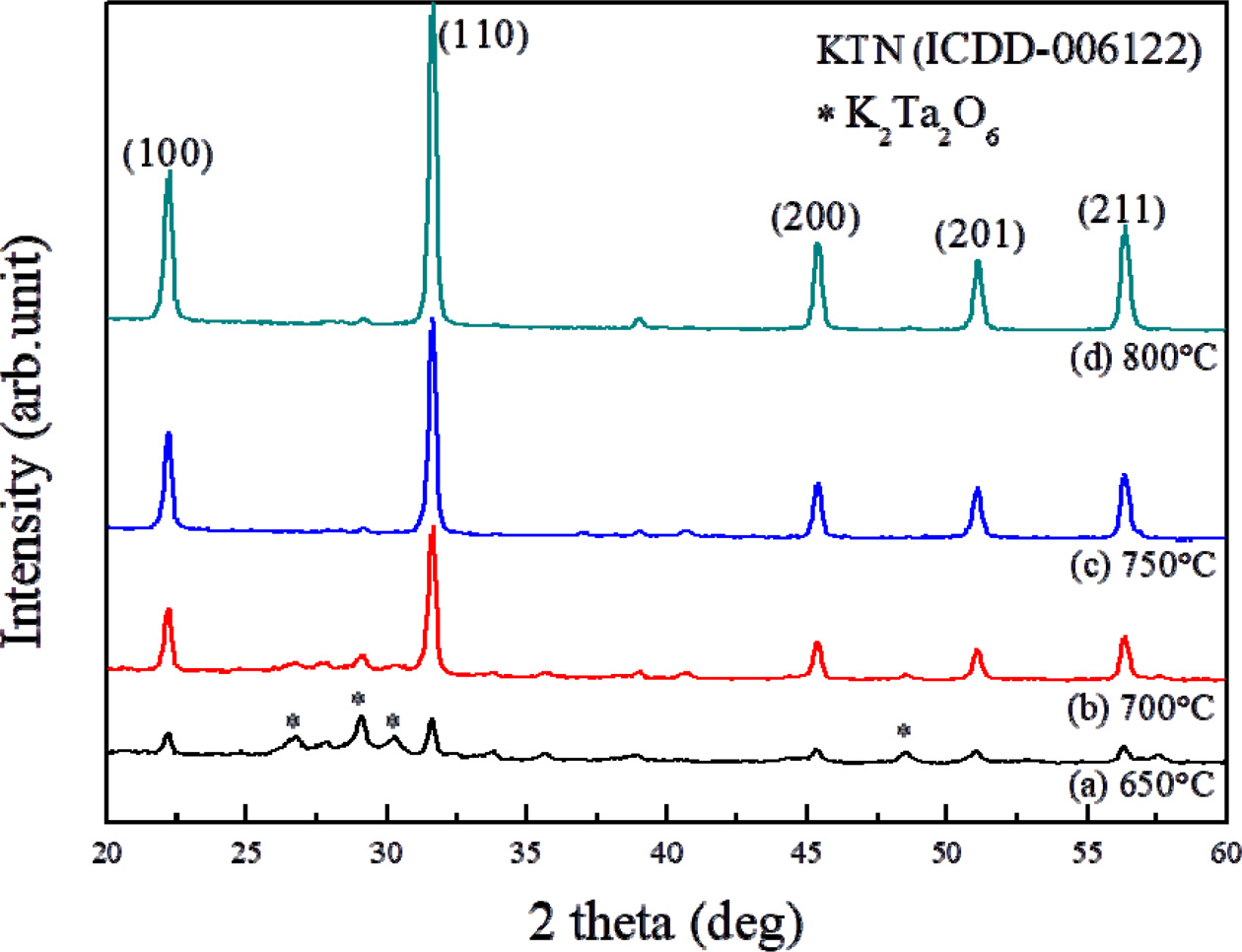
Fig. 1 shows the X-ray diffraction patterns of KTN thin
films according to sintering temperatures. The KTN thin films sintered at 650
degrees exhibited a coexistence of KTN crystal and K2Ta2O6
pyrocholre phases at an initial stage of crystallization. At a sintering
temperature of 700 oC, the peak of pyrochlore phase was greatly
reduced. In the thin films sintered at 750, 800, 850 oC, only
pure KTN phase were observed. The XRD peak’s intensity increased
and FWHM values decreased to 1.369, 0.364, 0.334, and 0.329 when
the sintering temperatures were raised. The thin films sintered at 750 oC
showed a cubic crystal structure with the lattice constants of a = 3.990 nm [14, 15].
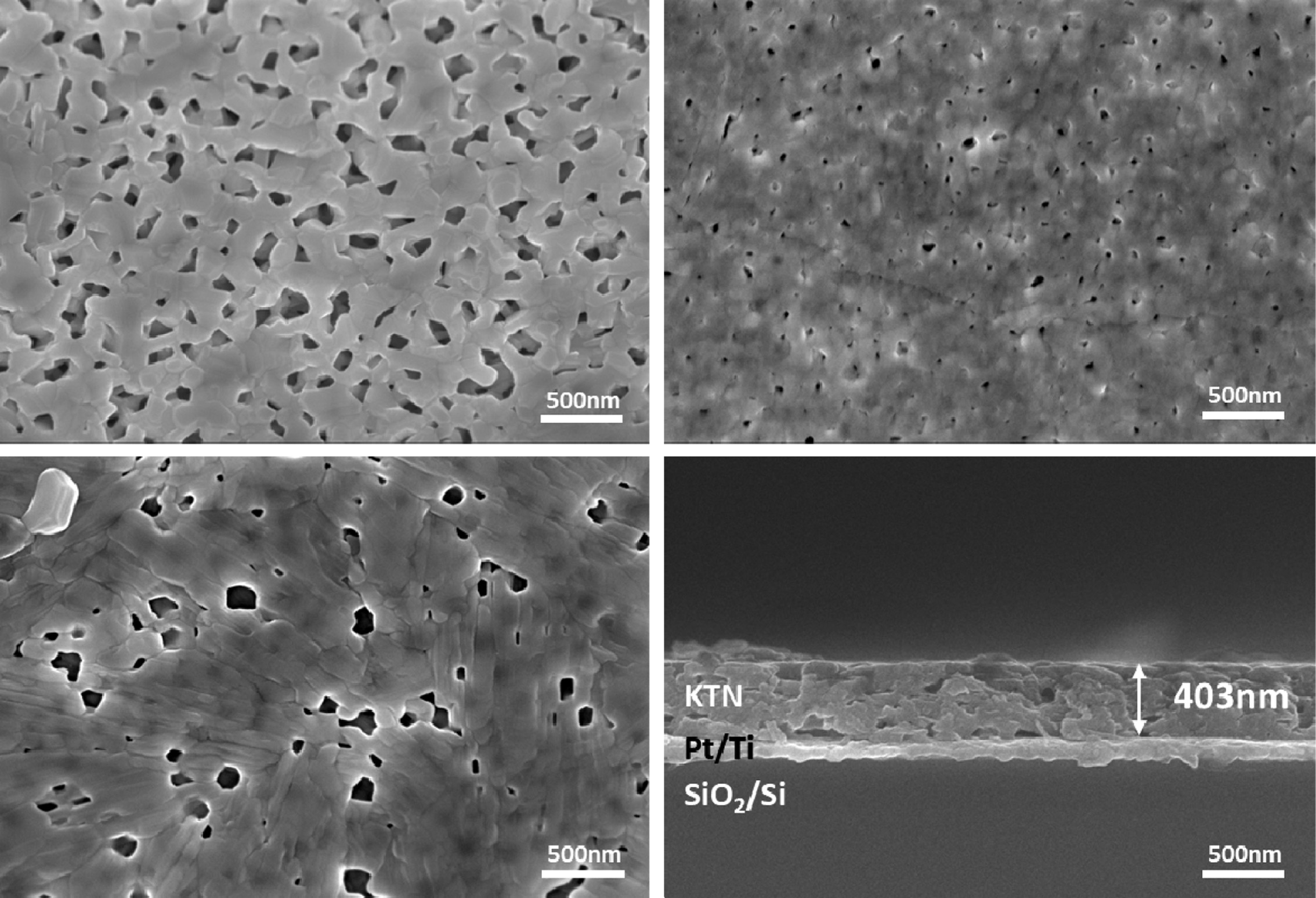
Fig. 2 shows the surface and cross-sectional micro- structures of thin KTN films by
sintered temperature. The thin films sintered at 650 oC showed
many pores and the secondary phase of K2Ta2O6
due to a low sintering temperature. In the specimen sintered at 700 degrees
(Fig. 2(a)), no secondary phase was observed. As the sintering temperature
increased, the pores decreased while the microstructure
was relatively dense. However, pores were distributed in
all thin films. In particular, the specimens sintered at 800 oC
(Fig. 2(c)) exhibited an increase in porosity due to volatilization of K
ion. The thin films sintered at 750 oC showed a dense and
flat cross-sectional microstructure (Fig. 2(d)). The average thickness of thin
KTN films was about 410 nm.
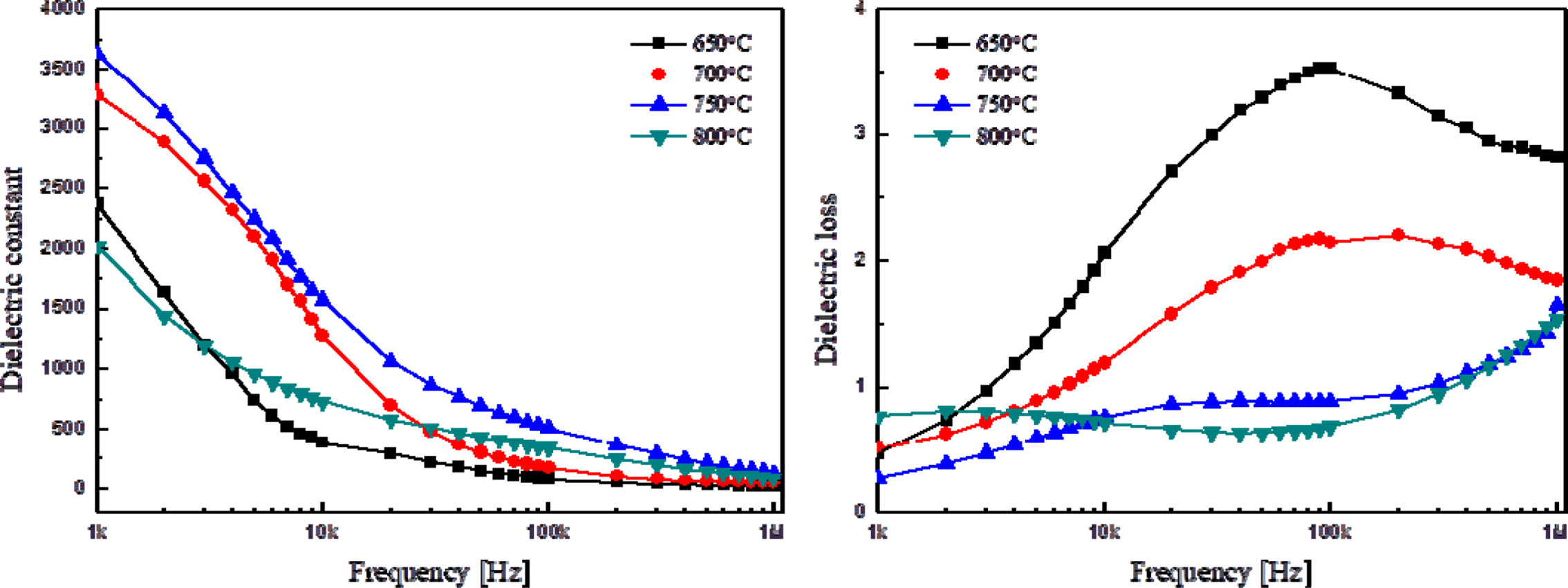
Fig. 3 shows the relative dielectric constant and loss of
thin KTN films by applied frequency. It shows the typical characteristic of
dielectric relaxation [16] in which the dielectric constant decreased when the frequency
was raised. The dielectric constant could have abruptly
decreased at an applied frequency of around 10 kHz due to the reduced
polarization of an internal space charge. The thin films sintered at 750 oC
showed good dielectric constant and loss properties. This is attributed to the
reduction of the pyrochlore phase and pores, as shown in Fig. 2 [17].
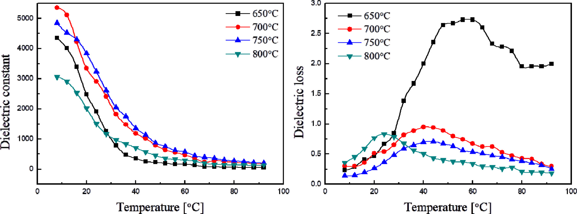
Fig. 4 shows the relative dielectric constant and loss of
KTN films at different temperatures. The relative dielectric constant decreased
when the temperature was raised within the range of 10 oC~90 oC,
while the maximum dielectric loss was around 20~40 oC. From
these properties, the phase transition temperature was considered to be
slightly lower than 10 oC. The phase transition temperature of
thin KTN films slightly increased when compared to that of bulk specimens of
the same composition (Tc=30 oC [18]). This seems to
have been caused by the stress generated at the interface between thin films
and substrates. The thin films sintered at 650 oC showed a high
dielectric loss due to the distribution of secondary phase and pores. The
relative dielectric constant and loss at 30 oC of the specimens
sintered at 750 oC showed excellent properties
of 3617 and 0.264, respectively.
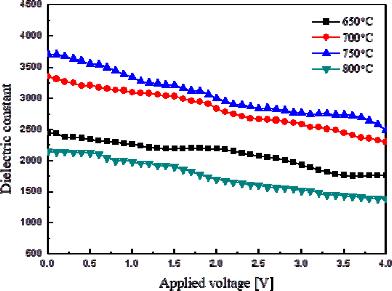
Fig. 5 shows the relative dielectric constant of thin KTN
films by applied DC voltage. The dielectric constant decreased
when the applied DC voltages was raised. This is
because the rotation and displacement of dipoles in the unit
lattice were suppressed by the applied DC voltage. The slope of dielectric
constant according to the DC voltage of the thin films sintered at 750 oC
was about -8.27 %/V.
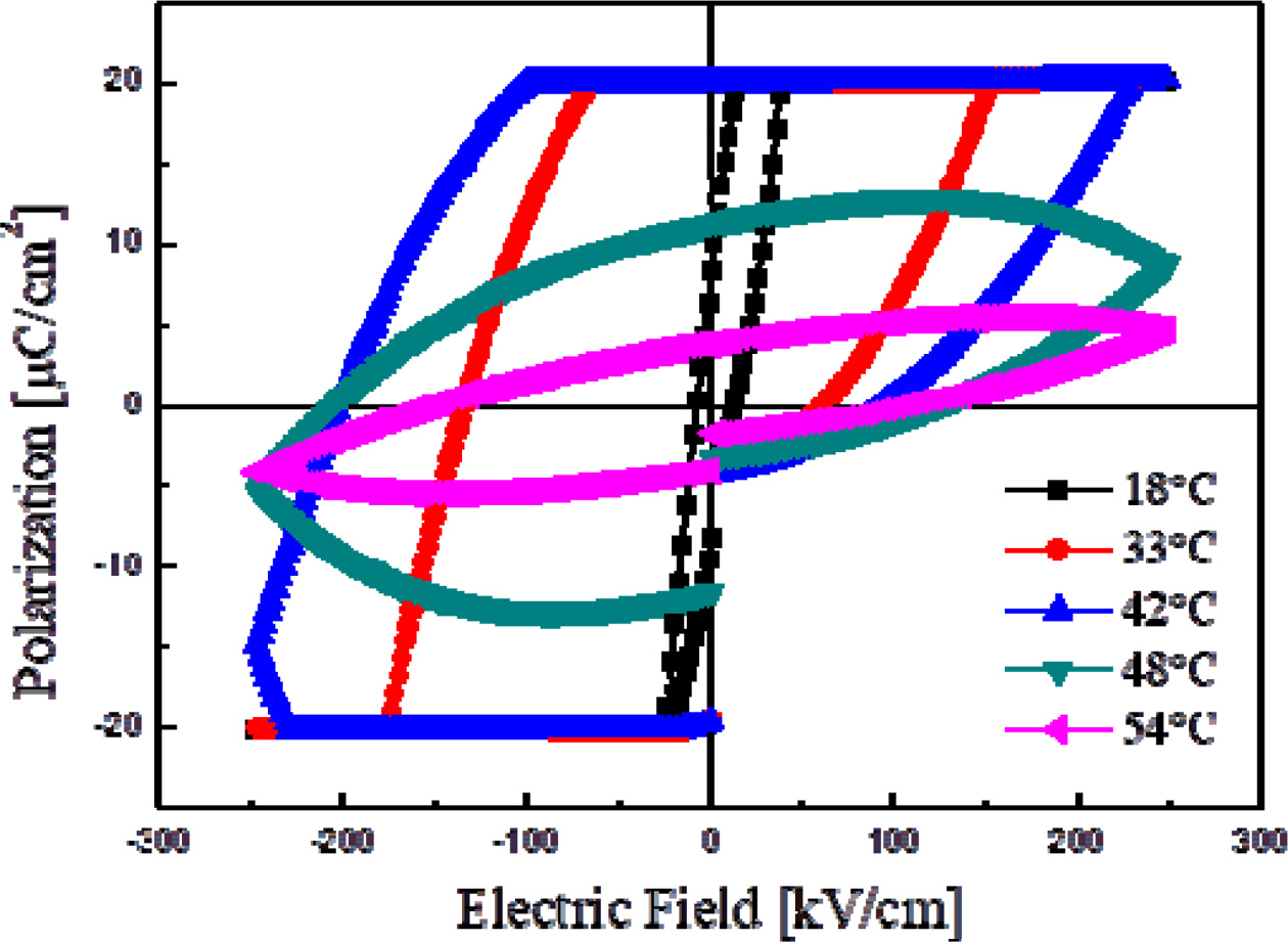
Fig. 6 shows the hysteresis loops of thin KTN films
sintered at 750 oC as a functional temperature. In the thin
films sintered at 650 oC, crystallization was not performed
due to a low sintering temperature, as shown in the XRD
properties of Fig. 1. The thin films sintered at 750 oC showed
the highest remanent polarization as well as coercive field properties of 20.0 μC/cm2,
and 122.6 kV/cm at 36 oC, respectively. When
the measured temperature became higher, the remanent
polarization and coercive fields decreased, while disorder in the dipole
arrangement increased. The ferroelectric properties of thin KTN
films were greatly influenced by pores and crystallinity in the secondary
phase.
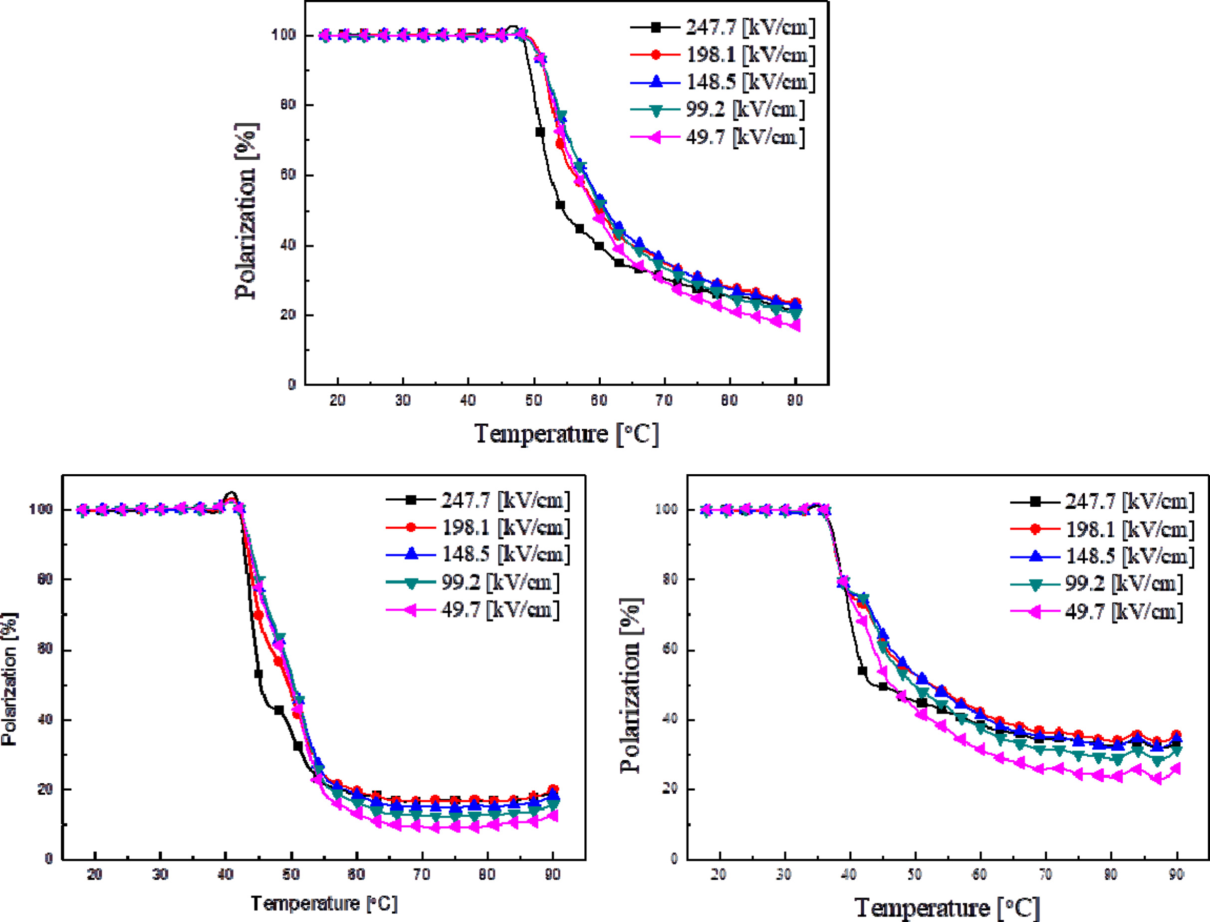
Fig. 7 shows the remanent polarization of thin KTN films
by temperature and applied voltage. While the remanent
polarization at 10 oC were fixed at the maximum value,
this figure shows the relative change in properties at different
temperatures. In the thin films sintered at 750 oC (Fig. 7(b)),
an abrupt decrease in remanent polarization was observed when the temperature
was changed. According to temperatures, materials with higher
crystallinity seem to have more sensitive electrical characteristics.
This could also be observed when single ferroelectric
substances displayed transition characteristics of the first
phase.
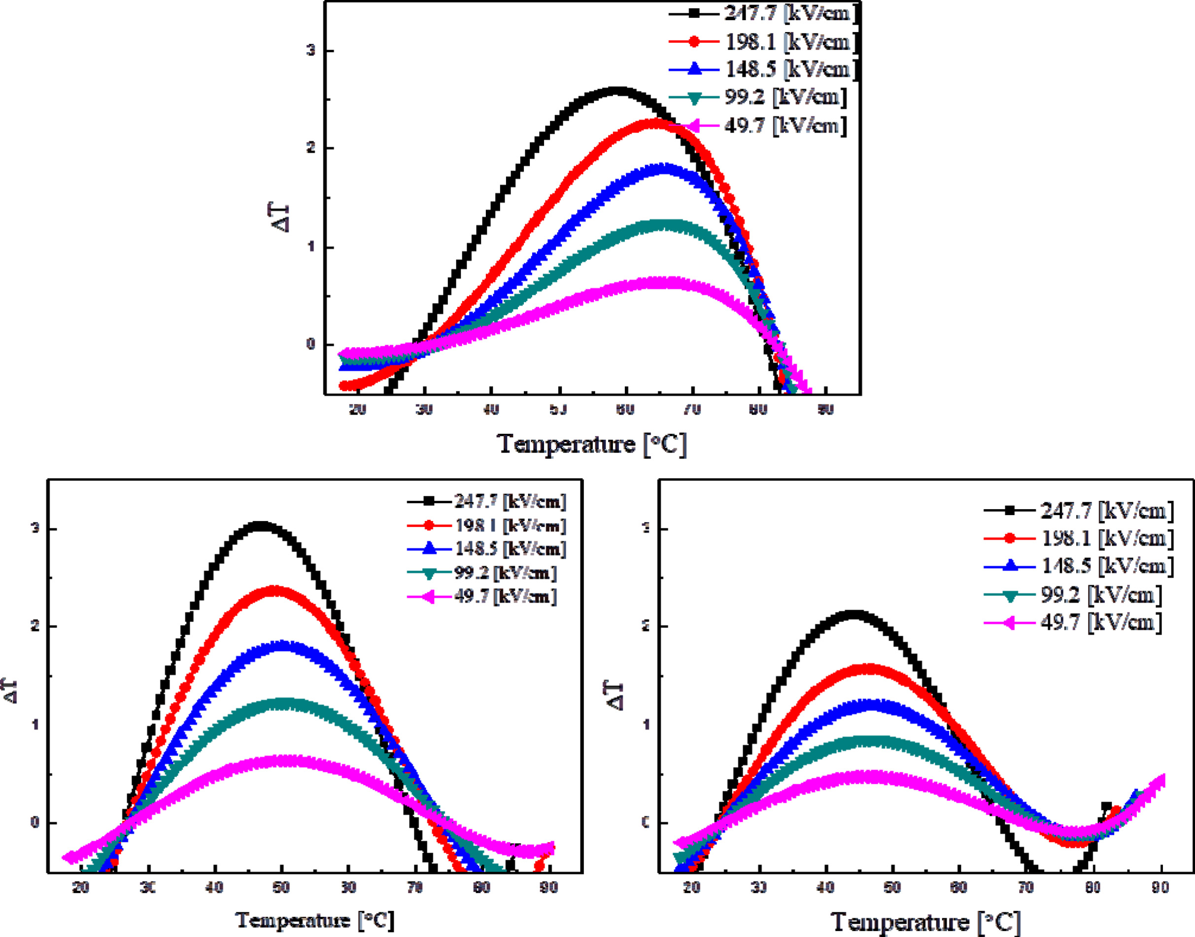
Fig. 8 shows the electrocaloric properties (ΔT) of thin
KTN films at different temperatures. When an electric field of 247 kV/cm was
applied to the specimens sintered at 750 oC, the highest electrocaloric
properties of 3.02 oC
was observed. In all specimens, the maximum
electrocaloric properties were obtained at the phase transition temperature of
around 50 oC,
which is higher than the Curie temperature. This could be attributed to
dipoles’ characteristics of field-induced polarization. This could also be
attributed to the application of an electric field close to the phase
transition temperature at which the ferroelectric and
dielectric phases coexisted [19]. The thin films sintered at 650 oC were not crystallized due to
a low sintering temperature and thus not applicable to a measurement of their
electrocaloric properties. The specimens sintered at 800 oC showed low electrocaloric
properties due to formation of pores caused by excessive sintering.
|
Fig. 1 X-ray diffraction patterns of K(Ta0.6Nb0.4)O3 thin films
according to the sintering temperature. |
|
Fig. 2 Surface and cross-sectional microstructures of K(Ta0.6Nb0.4)O3 thin films with the sintering temperatures; (a) surface, 700 o
C, (b)
surface, 750 o
C, (c) surface, 800 o
C and (d) cross-section, 750 o
C. |
|
Fig. 3 Relative dielectric constant and dielectric loss of K(Ta0.6Nb0.4)O3 thin films with the applied frequency. |
|
Fig. 4 Relative dielectric constant and dielectric loss of K(Ta0.6Nb0.4)O3 thin films. |
|
Fig. 5 Relative dielectric constant of K(Ta0.6Nb0.4)O3 thin films
with DC voltage applied. |
|
Fig. 6 Hysteresis loops of K(Ta0.6Nb0.4)O3 thin films sintered at
750 o
C. |
|
Fig. 7 Polarization of K(Ta0.6Nb0.4)O3 thin film with temperature and voltage application. |
|
Fig. 8 Electrocaloric properties (ΔT) of K(Ta0.6Nb0.4)O3 thin films with temperature changes. |
This study investigated the structural and electrical
properties of thin K(Ta0.6Nb0.4)O3 films for
their applicability to electrocaloric devices. In the specimen sintered at 650 oC, numerous pores and a
pyrochlore phase of K2Ta2O6 were observed.
Also, a peak of pure KTN crystalline was observed in the sintering at 750 oC. The porosity of specimens
sintered at 800 oC
increased due to the volatilization of K ion caused by an excessive
sintering temperature. The optimum sintering temperature of the
specimens was 750 oC. A rapid reduction of the dielectric constant at an
applied frequency of around 10 kHz could
have been caused by the decrease in polarization of space charge. According to
the temperatures, the higher crystallinity seems correlated to higher
ferroelectric properties. In all specimens,
the maximum electric energy was obtained at a temperature slightly higher than
the phase transition temperature.
This could be attributed to the dipoles characteristics of field-induced
polarization. This could also be attributed to the application of an electric
field close to the phase transition temperature at which the ferroelectric and
dielectric phases coexisted. Also, when an electric field of 247 kV/cm was
applied to the specimens sintered at 750 oC,
the highest electrocaloric properties of 3.02 oC
was observed.
This research was supported by Basic Science Research
Program through the National Research Foundation of Korea (NRF) funded by the
Ministry of Education (No. 2017R1D1A3 B03032164) and by Korea Institute of
Planning and Evaluation for Technology in Food, Agriculture, Forestry and
Fisheries (IPET) through Agriculture, Food and Rural Affairs Research Center
Support Program, funded by Ministry of Agriculture, Food and Rural Affairs
(MAFRA) (717001-7).
- 1. E. Jabry, G. Boissier, A. Rousset, R. Carnet, and A. Lagrange, J. Phys. Colloque. 47[Suppl.2] (1986) C1-843.
-

- 2. S. Guillemet-Fritsch, J.L. Baudour, C. Chanel, F. Bouree, and A. Rousset, Solid State Ionics 132 (2000) 63-69.
-
- 3. F.C.M. Driessens and G.D. Rieck, J. Inorg. Nucl. Chem. 28 (1966) 1593-1600.
-
- 4. J. Jung, J. Torfer, J. Murbe, and A. Feltz, J. Eur. Ceram. Soc. 6 (1990) 351-359.
-
- 5. H.J. Van Daal and A.J. Bosman, Phys. Rev. 158 (1967) 736-747.
-
- 6. S. Guillemet-Fritsch, C. Chanel, J. Sarrias, S. Bayonne, A. Rousset, X. Alcobe, and M.L. Martinez Sarrion, Solid State Ionics 128 (2000) 233-242.
-
- 7. J. Yang and X. Hao, J. Am. Ceram. Soc. 102[11] 6817-6826.
-
- 8. B. Liu, H. Zhang, Y. Zhang, X. Lv, Y. Yang, L. Wei, X. Wang, H. Yu, C. Zhang, and J. Li, Acta. Phys. Pol. A. 135 (2019) 396-400.
-
- 9. D. Fang, Z. Wang, P. Yang, W. Liu, and C. Chen, J. Am. Ceram. Soc. 89 (2006) 230-235.
-
- 10. J.L. Martin De Vidales, P. Garcia-Chain, R.M. Rojas, E. Vila, and O. Garcia-Martinez, J. Mater. Sci. 33 (1998) 1491-1496.
-
- 11. S.E. Shirsath, C. Cazorla, T. Lu, L. Zhang, Y.Y. Tay, X. Lou, Y. Liu, S. Li, and D. Wang, Nano. Lett. 20 (2019) 1262-1271.
-
- 12. M.N. Muralidharan, P.R. Rohini, E.K. Sunny, K.R. Dayas, and A. Seema, Ceramics International, 38 (2012) 6481-6486.
-
- 13. K.M. Kim, S.G. Lee, and M.S. Kwon, Journal of Ceramic Processing Research, 19 (2018) 302-305.
- 14. S. Hirano, T. Yogo, K. Kikuta, T. Morishita, and Y. Ito, J. Am. Ceram. Soc. 75[6] (1992) 1701-1704.
-
- 15. A.X. Kuang, C.J. Lu, G.Y. Huang, and S.M. Wang, J. Cryst. Growth. 149[1-2] (1995) 80-86.
-
- 16. E.L. Dereniak and D.G. Crowe, “Optical radiation detectors”, John Wiley & Sons (1984).
- 17. F.M. Pontes, E.R. Leite, E. Longo, J.A. Varela, E.B. Araujo, and J.A. Eiras, Appl. Phys. Lett. 76[17] (2000) 2433-2435.
-
- 18. V.M. Joseph, L.M. Adolph, W.S. Norman, B.C. Antonio, Y.L. Chen, A.W. Richard, and A.W. Curtis, J. Appl. Phys. 72[2] (1992) 615-619.
-
- 19. D. Hennings, A. Schnell, and G. Simon, J. Am. Ceram. Soc. 65[11] (1982) 539-544.
-
 This Article
-
2020; 21(6): 725-730
Published on Dec 31, 2020
- 10.36410/jcpr.2020.21.6.725
- Received on Jun 12, 2020
- Revised on Sep 3, 2020
- Accepted on Oct 6, 2020
Services
- Abstract
introduction
experimental
results and discussion
conclusions
- Acknowledgements
- References
- Full Text PDF
Shared
Correspondence to
- Sung-Gap Lee
-
Dept. of Materials Engineering and Convergence Technology, RIGET, Gyeongsang National University, Jinju 52828, Korea
Tel : +82-55-772-1687 Fax: +82-55-772-1689 - E-mail: lsgap@gnu.ac.kr
Clean-Energy Research Institute(CRI), Hanyang University, 222, Wangsimni-ro, Seongdong-gu, Seoul, 04763, Korea
E-mail: jcpr@hanyang.ac.kr