


- Phases and morphorlogy of CuFeS2 films prepared by electrodeposition
Ming Ji, Kegao Liu* and Nianjing Ji
School of Materials Science and Engineering, Co-Innovation Center for Green Building of Shandong Province, Shandong Jianzhu University, Fengming Road, Jinan 250101, China
This work reports one
low-priced ways for production of CuFeS2 films on conductive glass
surface. CuFeS2 films were prepared by electrodeposition and
post-sulfurization treatment at 220 oC for 30 h in N2
atmosphere for the first time. CuFeS2 films were prepared by
electrodeposition with sulfate, ascorbic acid, complexing agent sodium citrate
as raw materials. When the deposition potential is -1.0 V and the
deposition time is 20 min, CuFeS2 thin films with good phrase
formation can be obtained at pH 4 and 0.02M Na2S2O3·H2O.
The phase of samples were characterized using X-ray diffraction (XRD). The
morphology of samples were characterized via scanning electron microscopy
(SEM). The composition of samples were characterized by energy dispersive
spectrometer (EDS). The crystallinity of CuFeS2 thin films prepared
under these conditions are relatively good. The microcosmic morphology of the
samples is flaky crystal. It is shows that post-sulfurization method is helpful
for the phase formation of CuFeS2 films electrodeposited.
Keywords: CuFeS2, Thin film, Photoelectric, Electrodeposition, Solar energy
Recently, Chalcopyrite CuFeS2 was classified as
indispensable and multi-functional materials [1] due to their abundance [2],
their higher conversion efficiency [3], higher absorption
coefficients [3] and lower toxicity [2, 3] compared with other
semiconducting materials. It was found to be a semiconductor with a zero or
narrow band gap [4]. It has been considered as a prospective material
with wild applications including energy storage, solar
energy generation [5-8]. The preparation methods of optoelectronic materials
including chemical co-reducton [9], vacuum evaporation
[10], solution-chemical method [11-13], hydro-thermal
method [3, 5, 8, 14], electrodeposition [15], flash evaporation technique [4],
high energy ball milling [16, 17], thermal-injection synthesis [2] and so on.
Se Hoon Kim studied the influence of surface roughness on
the efficiency of a flexible organic solar cell [18]. At the same time,
Cuan-Lin Chiu researched the influence of doping iron ions into Cu(In,Ga)Se
films [19]. Thin-film batteries also has been studied for a long time. Kegao
Liu has prepared many kind of absorption layer films, such as CuInSe2
[20], CuInS2 [21] and ZnS [22] successfully, for example. As a kind
of ternary optoelectronic material, CuFeS2 has strict technological
requirements in the preparation process, and the process parameters of
electrodeposition have great influence on the properties of CuFeS2
preparation [15], so it is necessary to explore an optimum techno- logical condition.
Eelectrodeposition method has the advantages of non-vacuum
and low cost, the deposition process can be carried out at room temperature,
and a uniform and dense film can be prepared [15]. The thin film can be
crystallized by the sulfurization treatment, and the film is
crystal structure of chalcopyrite. The electrodeposited CuFeS2
is often prepared by sulfurization treatment to improve the composition and
crystallization, thus improving the photoelectric performance of the film.
This work used CuSO4·5H2O, (NH4)2Fe(SO4)·6H2O,
and Na2S2O3·H2O as the basic raw
material, CuFeS2 thin films were prepared by using the constant
potential method. The effects of the pH value and the con- centration of Na2S2O3·H2O
on the phase formation and morphology of the
films were investigated and characterized.
Solution preparation: 0.01 M CuSO4·5H2O,
0.01 M (NH4)2Fe(SO4)·6H2O,
0.01 M ascorbic acid, 0.01 M complexing agent sodium citrate and a
certain con- centration of Na2S2O3·H2O.
The CuFeS2 thin films were electrodeposited at different pH and
concentra- tions of Na2S2O3·H2O
on the FTO-coated glass surface. The deposition time was 20 min and
deposition potential was -1.0 V. The films were prepared via using
electrodeposition and post-sulfurization at 220 oC for
30 h in an N2 atmosphere. The electrodeposition of thin films
was obtained via the PARSTAT 2273 electroche-mical workstation. All the experiments can be guaranteed
to be variable unique.
The crystal structure of samples were analyzed by the
Bruker D8 Advance XRD system with Nifiltered Cu-Kα (λ=1.5059 Å).
The samples’ surface morphology were analyzed by using
scanning electron microscope (SEM) with a model of JSM-7610F made by Japan
Electronics Co., Ltd. The composition of the film was detected by using energy
dispersive spectrometer (EDS) with a model of JSM-7610F made by Japan
Electronics Co., Ltd. The resistivity was measured by Four Probe Resistivity
Meter.
The
effect of pH of system on phase formation and morphology of CuFeS2
thin films
The crystal structures of the synthesized products were
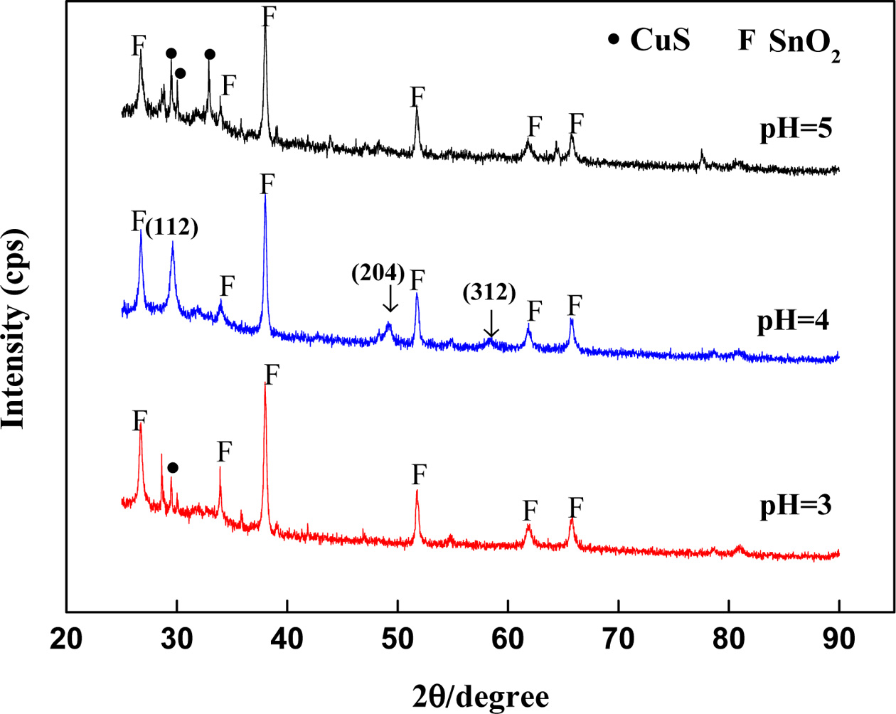
characterized by XRD. Fig. 1 shows the XRD patterns of
CuFeS2 thin films deposited on FTO substrate. FTO
substrate is one kind of conductive glass. Through the phase retrieval, it can
be seen that there are three peaks at 2θ angles with 29°, 48° and 57°. These
three peaks are matched with the three strong peaks of copper iron sulfide. The
peaks correspond to (112), (204) and (312) crystal planes of the chalcopyrite
structured CuFeS2 (Card No.74-1737) at pH 4, which is in consistent
with other reports [5]. Additional peaks resulting from FTO (mostly SnO2,
Card No.46-1088) have been identified as F. Each phase of the sample contains a
glass substrate. It may account for the thickness of the film. It can also be
observed from the Fig. 1 that the impurity phase CuS (Card No.75-2233) appears
in the other samples except the sample with pH 4. Only at pH 4 can the pure
phase of the target product be obtained. Therefore, the optimal pH value of the
system is 4.
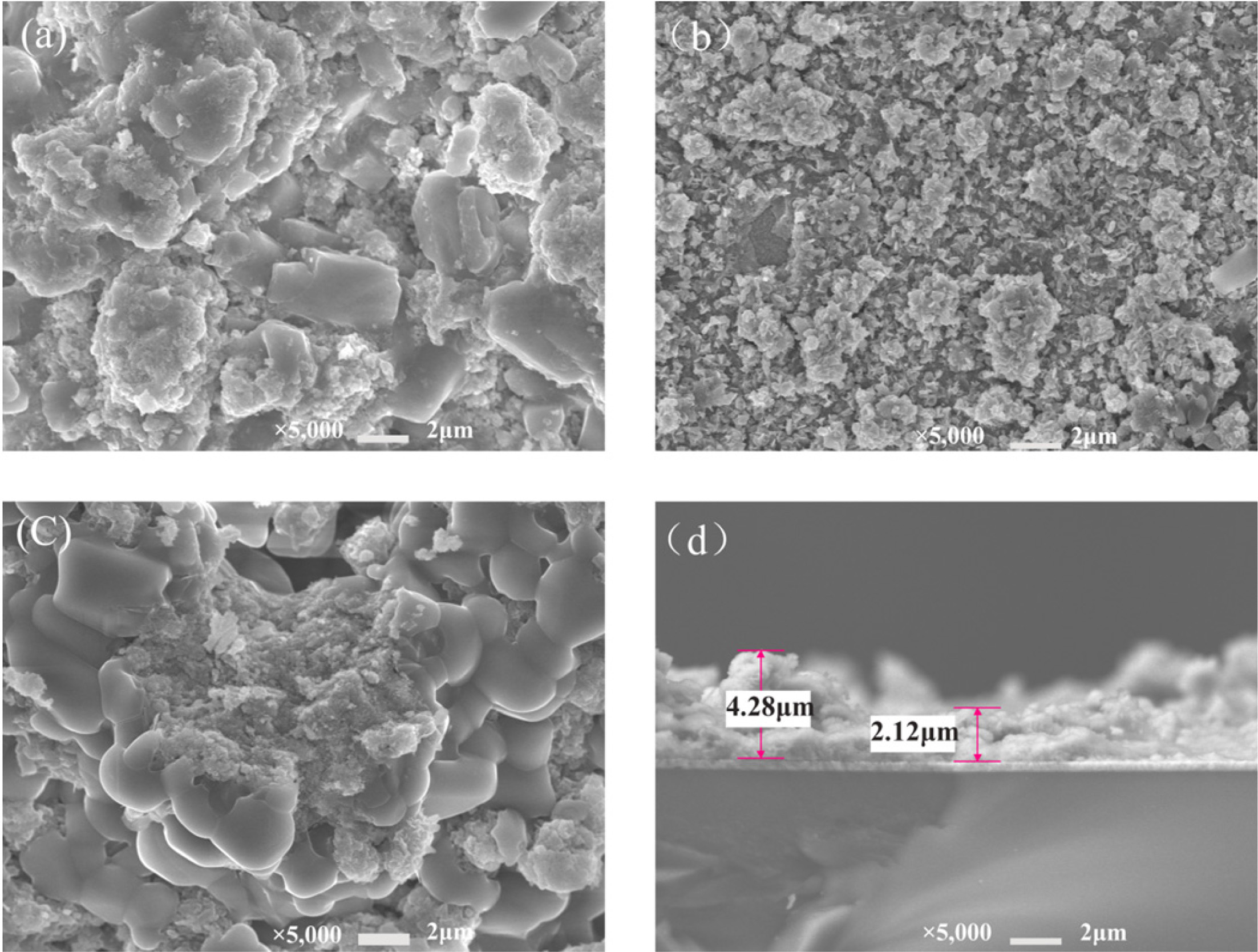
Fig. 2 shows the morphology of the synthetic CuFeS2
prepared by electrodeposition after sulfurization. It was found that the
surface of the film was relatively uniform, the degree of crystallization was
relatively good, and the particles were relatively small at pH 4. It can be
seen the microcosmic morphology of the samples is flaky crystal. The thickness
of the thin film varied from 1 to 5 μm.
For the above study, it is concluded that the structure
and morphology of films depend on pH mostly.
The
effect of concentration of Na2S2O3·H2O
on phase formation and morphology of CuFeS2 thin films
The crystal structures of the synthesized products were
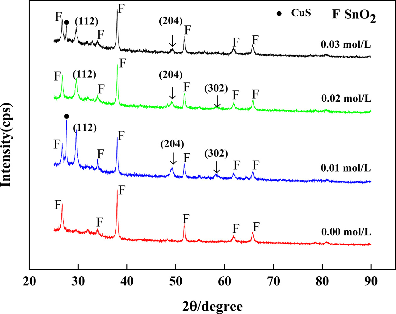
characterized by XRD. Fig. 3 shows XRD patterns of CuFeS2
thin films with different concentration of Na2S2O3·H2O
after sulfurization. It can be seen that there are three diffraction peaks at 2θ
angles with 29°, 48° and 57°, except that the concentration of Na2S2O3·H2O
is 0.00 M. These three peaks are matched with the three
strong peaks of copper iron sulfide. The diffraction peaks correspond to (112),
(204) and (312) crystal planes of the chalcopyrite structured CuFeS2
(Card No.74-1737), additional peaks resulting from FTO (mostly SnO2,
Card No.46-1088) have been identified as F. It can also be observed from the
Fig. 3 that the impurity phase CuS (Card No.74-1234) appears in sample of
0.01 M and 0.03 M. It is concluded that the purity phase could be
prepared when sample’s concentration of Na2S2O3·H2O
is 0.02 M. Therefore, the optimal concentration of Na2S2O3·H2O
is 0.02 M.
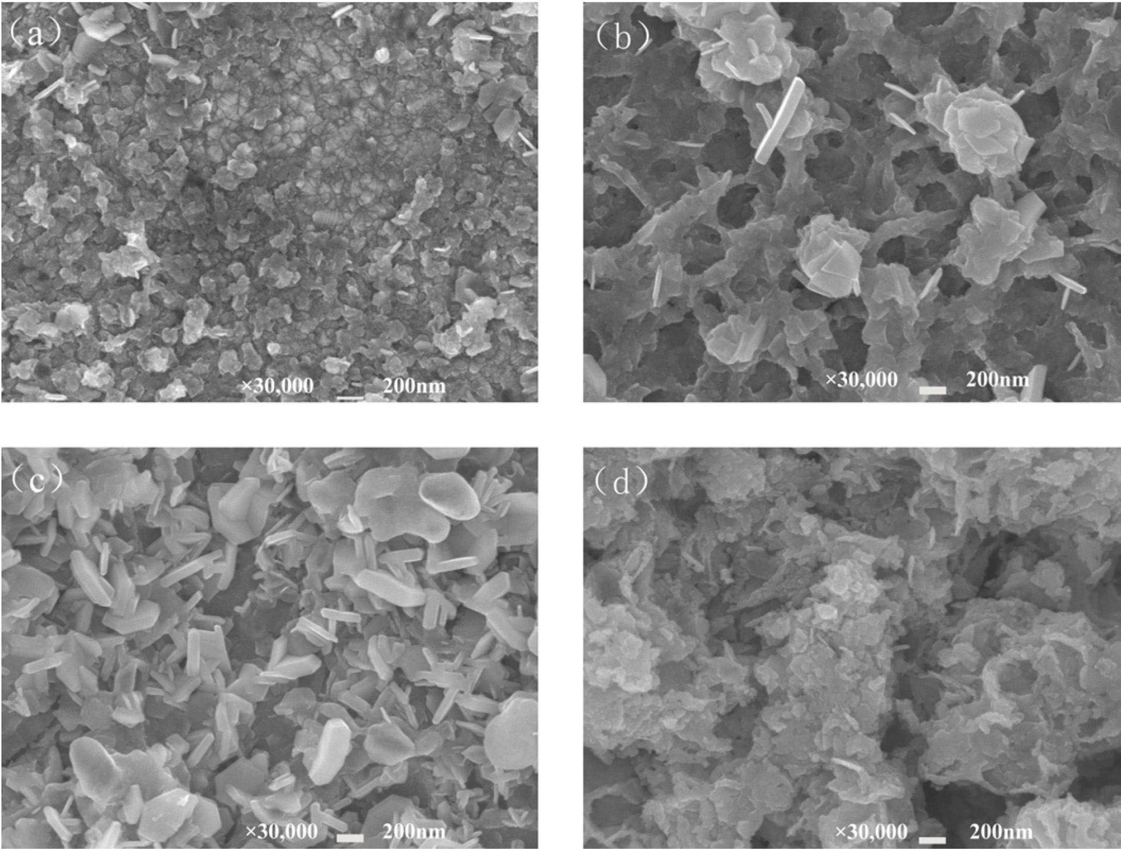
Fig. 4 shows the morphology of the synthetic CuFeS2
prepared by electrodeposition after sulfurization. It was found that all the
samples showed flake products except that the concentration of Na2S2O3·H2O
is 0.00 M. In order to determine the composition of the flake
product further, the energy spectrum of the flake target product was detected.
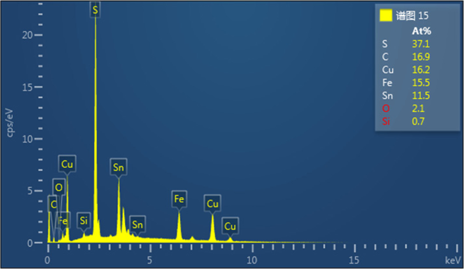
From Fig. 5, it was found that the ratio of copper - iron
- sulfur atom was roughly in accordance with the atomic ratio of the target
product 1:1:2. The thin film’s resistivity is 2.016 Ω·cm.
|
Fig. 1 XRD patterns of thin films prepared at pH 3-5 after sulfurization. |
|
Fig. 2 Morphology of samples prepared by electrodeposition after sulfurization. (a) pH = 3; (b) pH = 4; (c) pH = 5; (d) Cross section of thin film. |
|
Fig. 3 XRD patterns of thin films prepared with different of Na2S2O3·H2O after sulfurization. |
|
Fig. 4 Morphology of samples prepared by electrodeposition after sulfurization.(a) 0.00 M; (b) 0.01 M; (c) 0.02 M; (d) 0.03 M. |
|
Fig. 5 EDS spectrum showing the elemental composition of synthetic CuFeS2. |
In summary, CuFeS2 films has been prepared
successfully on conductive glass surface by two-step approach:
electrodeposition and post-sulfurization. CuFeS2
films were prepared by electrodeposition and post-sulfurization treatment at
220 oC for 30 h in N2 atmosphere. There are
four highlights in this work. The first one, when deposition potential is
-1.0 V and the deposition time is 20 min, CuFeS2 thin
films can be obtained at pH 4 and 0.02 M Na2S2O3·H2O.
Secondly, the crystallinity of CuFeS2 thin films prepared under
these conditions are relatively good. The microcosmic morphology of the samples
is flaky crystal by SEM. Furthermore, the sample’s phase has been confirmed as
chalcopyrite structure. At the same time, the ratio of copper - iron - sulfur
atom by EDS was roughly in accordance with the atomic ratio of the target
product. These results are meaningful for proving that post-sulfurization is a
useful measure for preparation of CuFeS2 films.
This work was financially supported by the National
Natural Science Foundation of China (No.51272140) and the Innovation Team of
the Co-Innovation Center for Green Building of Shandong Province in Shandong
Jianzhu University.
- 1. N. Wu, Y. Li, M. Zeng, J. Gao, Y. Tang, Z. Zeng, Y. Zheng. J. Solid State Chem. 271(2019) 292-297.
-

- 2. E. Bastola, K.P. Bhandari, I. Subedi, N.J Podraza, Randy J Ellingson. MRS Commun. 8[3] (2018) 970-978.
-
- 3. S. Sil, A. Dey, S. Halder, J. Datta, P.P. Ray. J. Mater. Eng. Perform. 27[6] (2018) 2649-2654.
- 4. B. Korzun, A. Galyas. J. Electron. Mater. 48[5] (2019) 3351-3354.
- 5. K.M. Deen, E. Asselin. Electrochim. Acta. 297 (2019) 1079-1093.
-
- 6. Q. Jiang, R. Chen, X. Guo, Y. Zhu, W. Cheng, W. Li, X. Yang, H.C. Chen. Sol. Enrgy. 179 (2019) 59-66.
-
- 7. I.S. Lyubutin, C.-R. Lin, S.S.Y.-J. Siao, M.O. Shaikh, K.O. Funtov, S.C.S. Wang. ACTA Mater. 61[11] (2013) 3956-3962.
-
- 8. K.M. Deen, E. Asselin. Electrochimica. Acta. 212 (2016) 979-991.
-
- 9. K. Liu, J. Li, Y. Xu, H. Li, W. Gao. Results. Phys. 11 (2018) 749-754.
-
- 10. L. Barkat, N. Hamdadou, M. Morsli, A Khelil, J C Bernède. J. Cryst. Growth. 297[2] (2006) 426-431.
-
- 11. P. Kumar, S. Uma and R. Nagarajan. Chem. Commun. 49[66] (2013) 7316-7318.
-
- 12. Y.-H.A.Wang, N.Bao, A. upta. Solid State Sci. 12[3] (2010) 387-390.
-
- 13. D. Liang, J. Li, and G. Pang. J. Mater. Sci. 51[11] (2016) 5412-5420.
- 14. H. Yu, J. Xu, Y. Hu, H. Zhang, C. Zhang, C. Qiu, X. Wang, B. Liu, L. Wei, J. Li. J. Mater. Sci.: Mater. Electron. 30[13] (2019) 12269-12274.
- 15. J. Zhou, S. Yu, X. Guo, L. Wu, H. Li. Curr. Appl. Phys. 19[2] (2019) 67-71.
-
- 16. N. Poloko, G. Danha, T. Gaogane. Procedia Manufacturing. 35 (2019) 488-493.
-
- 17. A.O. Moghaddam, A. Shokuhfar, P. Guardia,Y. Zhang, A. Cabot. J. Alloy. Compd. 773 (2019) 1064-1074.
-
- 18. S.H. Kim, D.Y. Lee, Y.-J. Oh. J. Ceram. Process. Res. 21[1] (2020) 42-49.
- 19. C.-L. Chiu, T. Subburaj, S. Som, C.-Y. Ou, C.-H. Lu. J. Ceram. Process. Res. 18[10] (2017) 754-759.
- 20. K. Liu, Y. Xu, Q. Sun, H. Li, H. Wu. Results. Phys. 12 (2019) 766-770.
-
- 21. K. Liu, J. Li, Y. Xu, L. Shi, W. Gao. Cryst. Res. Technol. 53[2] (2018)1700203.
-
- 22. K. Liu, W. Song, Y. Xu, J. Li, Z. Wang. J. Ceram. Process. Res. 19[2] (2018) 146-149.
 This Article
-
2020; 21(4): 456-459
Published on Aug 30, 2020
- 10.36410/jcpr.2020.21.4.456
- Received on Feb 6, 2020
- Revised on Mar 24, 2020
- Accepted on Apr 2, 2020
Services
- Abstract
introduction
experimental details
results and discussion
conclusions
- Acknowledgements
- References
- Full Text PDF
Shared
Correspondence to
- Kegao Liu
-
School of Materials Science and Engineering, Co-Innovation Center for Green Building of Shandong Province, Shandong Jianzhu University, Fengming Road, Jinan 250101, China
Tel : ++86 15610183153 - E-mail: liukg163@163.com
Clean-Energy Research Institute(CRI), Hanyang University, 222, Wangsimni-ro, Seongdong-gu, Seoul, 04763, Korea
E-mail: jcpr@hanyang.ac.kr