


- High-Electric-Field-Induced strain at a low driving field in lead-free 0.78Bi0.5Na0.5TiO3-0.22SrTiO3 ceramics modified with KNbO3
Duc Thang Le, Seong Won Kim, Subramanian Sasikumar and Jeong Ho Cho*
Electronic Convergence Materials Division, Korea Institute of Ceramic Engineering & Technology, Jinju-si, Gyeongsangnam-do 52851, South Korea
This article is an open access article distributed under the terms of the Creative Commons Attribution Non-Commercial License (http://creativecommons.org/licenses/by-nc/4.0) which permits unrestricted non-commercial use, distribution, and reproduction in any medium, provided the original work is properly cited.
Toward the development of piezoelectric actuators, single-perovskite-structure 0.78Bi0.5Na0.5TiO3-(0.22-x)SrTiO3-xKNbO3 (BNT-ST-xKN, withx=0–0.03) lead-free piezoelectric ceramics were prepared by a conventional solid-state reaction method, and the effects of KN substitution on the microstructure and electrical properties were investigated. FE-SEM observations revealed that the grain size of the sintered specimens decreased upon KN replacement. The temperature dependence of the relative dielectric permittivity (εr–T) curves showed that the ferroelectric-to-relaxor transition temperature (TF-R) decreased from 55 oC for x=0 to below room temperature for x≥0.01. The hysteresis loop became slim, with the strain initially increasing and then decreasing with an increase in the KN content. Notably, at x= 0.01, a large unipolar field-induced strain (Smax) of up to 0.157% with corresponding normalized strain d33* (Smax/Emax) of 785 pm/V was achieved at 2 kV/mm. The high strain under an ultra-low electric field was attributed to the local chemical inhomogeneity of the constituent elements, which was further confirmed by backscattered electron (BSE) and EDX mapping analyses.
Keywords: Actuator, Bismuth-based, Electromechanical strain, Lead-free, Piezoelectric.
The importance of electronic materials has been increasing alongside the development of the electronic industry. Piezoelectric ceramics play important roles in sensors, actuators, ultrasonic motors, and energy storage devices [1, 2]. Thus far, most piezoelectric devices have utilized lead-based materials such as Pb(Zr1-xTix)O3 (PZT) ceramics due to their superior piezoelectric responses [3, 4]. However, the evaporation of lead oxide (PbO), which is harmful to both the global environment and human health, has led to the implementation of regulations restricting the use of such hazardous materials in electronic products [3, 5]. Therefore, considering the environmental and health concerns associated with lead-based materials, it is of great importance to develop environmentally friendly lead-free piezoelectric materials. Hence, lead-free ceramics with an ABO3 perovskite structure, such as (Na, K)NbO3 (NKN), (Bi, K)TiO3 (BKT), BaTiO3 (BT), (Ba, Zr)TiO3 (BZT), and (Bi, Na)TiO3 (BNT), have been studied extensively [6-8]. In terms of actuator applications, BNT with a relatively high TC (~300 °C) and a large strain is a promising substitute for lead-based ceramics [9-11]. However, in experimental works, the electrical and electromechanical properties of BNT solid compounds have been found to be inferior to those of lead-based materials. Another challenge is that while most PZT-based piezo-actuators operate under an electric field of 2-3 kV/mm, BNT ceramics typically require a higher driving electric field (~6 kV/mm) due to their large coercive field and high conductivity [5, 12-14]. Thus, lowering the triggering field in BNT-based ceramics while maintaining their substantial piezoelectric response is of vital importance for practical applications.
It is widely accepted that the electrical properties of piezoceramics can be improved by the formation of morphotropic phase boundaries (MPB) between two solid solutions [15-17]. Particularly, combinations of other perovskite compounds such as BT, BZT and BKT with BNT-based materials within MPB region have revealed significantly improved electrical performance capabilities compared to pure BNT [17-22]. For instance, by adding BT into BNT ceramics and adjusting the sintering conditions, a displacement larger than 1 µm was demonstrated by Choet al. [23]. Similarly, a large normalized strain (d33*) value of 767 pm/V was reported for 0.82BNT–0.18BKT system, synthesized by a conventional solid reaction route [22]. Nevertheless, such electromechanical properties commonly require high triggering fields (4–5 kV/mm), remaining a great issue for practical applications.
Recent findings have shown that SrTiO3 (ST) is more symmetric and suitable for incorporation with BNT, as ST-modified BNT ceramics exhibit high electromechanical strain (referred to as incipient piezoelectricity) under a relatively low electric field [24]. Consequently, over the past decade, much attention has been devoted to the development of BNT-ST with a low triggering field for industrial actuators. For example, a d33* value of 600 pm/V under an electric field of 4 kV/mm for BNT-25ST bulk materials was reported by Acosta et al. in 2014 [18, 19]. Later, Zhou et al. demonstrated a d33* value of 850 pm/V at 3 kV/mm for a NaNbO3-doped BNT-ST system, comparable to that of PZT-based ceramics [20]. In a study of (0.99-x)Bi1/2Na1/2TiO3-0.01KTaO3-xSrTiO3 (BNT-KT-100xST), a d33* value of 793 pm/V under an identical driving field was reported by Lee et al. [25]. Furthermore, an exceedingly high d33* value of 880 pm/V at 2 kV/mm was highlighted by his research group in a recent publication [26]. Although the mechanism of high piezoresponses remains to be clarified, these experimental results demonstrate a potential approach by which to achieve high electromechanical strains under relatively low external electric fields by incorporating appropriate modifiers into the BNT-ST host system.
KNbO3 (KN) is considered to be an excellent candidate as a lead-free ferroelectric material due to its large spontaneous polarization (Ps~30 µC/cm2) and high TC (> 400 ℃) [27]. It has also been reported that the addition of KN to BNT significantly enhances the electric-field-induced responses [28]. Therefore, with the aforementioned objective, we sought to modify BNT-ST with KN in this study. The effects of KN doping on the phase, microstructural and electro-strain properties of BNT-ST-based ceramic materials were investigated.
0.78Bi0.5Na0.5TiO3-(0.22-x)SrTiO3-xKNbO3 (x=0.00, 0.01 and 0.03) ceramics (abbreviated as BNT-ST-xKN) were prepared via a solid-state reaction method. High-purity raw materials of Bi2O3 (99.99%), Na2CO3 (99%), TiO2 (rutile; 99.99%), SrCO3 (99.9%), K2CO3 (99.99%) and Nb2O5 (99.9%) sourced from Kojundo Chemical Laboratory Co., Ltd., Japan, were chosen as the raw materials. These powders were weighed precisely to the aforementioned stoichiometric formula and were ball-milled for 24 h with ethanol using zirconia balls. The resulting slurries were subsequently dried at 100 ℃ (24 h), following by calcination at 850 ℃ for 2h. After grinding and sieving using a sieving apparatus with an aperture size of 75 µm, the calcined powders were pressed into disk-shaped pellets with a diameter of 10 mm and a thickness of 1.3 mm. All specimens were then sintered in covered alumina crucibles at 1150 ℃ for 2 h.
The crystallographic structure of the ceramics was examined using an X-ray diffractometer (XRD, RAD III, Rigaku, Japan). Field-emission scanning electron microscopy (FE-SEM, JSM-6700F, JEOL, Japan) was utilized to study the surface morphology of the sintered samples. To examine the electrical properties, the specimens were lapped to a thickness of 1 mm and an electrode was formed by printing silver paste onto both surfaces. The polarization-electric field (P-E) hysteresis loops and strain-electric field (S-E) curves were measured using a ferroelectric test system (Radiant P-LC-K, USA). An impedance analyzer (model HP4192A, Agilent Technologies, Inc., Japan) coupled with a temperature-controlled chamber (model 9023, Delta Design, UK) was employed to determine the relative dielectric permittivity (εr) and dielectric loss (tan δ) as functions of the frequency and temperature.
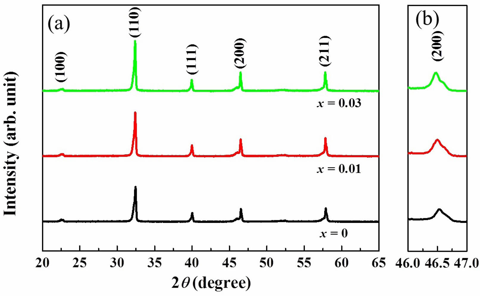
Fig. 1a shows XRD patterns in the 2θ range of 25–65o measured at room temperature (RT) for BNT-ST-xKN ceramics sintered at 1150 ℃. All specimens demonstrated a pure perovskite structure without any trace of a secondary phase. This pure perovskite phase confirmed that KN had completely diffused into the BNT-ST host lattice to form a new homogenous solid solution. For the core BNT-ST (x=0) ceramic, a single (200) peak is clearly observed in the range of 46º~47º (Fig. 1b), allowing classification as a pseudocubic structure. This XRD result is in agreement with those of previous studies of BNT-ST ceramics [18, 19, 29]. In BNT-ST compounds, the pseudocubic structure stems from the combination of a rhombohedral (BNT) structure and a cubic ST phase [18, 19, 25]. However, the enlarged XRD patterns in Fig. 1b indicate that the BNT-ST pseudocubic phase remains unchanged regardless of increases in the KN level (x), suggesting that the addition of KN has little effect on the phase transition, although its composition possesses an orthorhombic symmetry [30]. Otherwise, the net effect of KN modifier on the XRD patterns is revealed by a shift of (200) peak towards a lower angle (Fig. 1b). It is reasonable to accept that this shift is due to the replacement of the smaller ions (Sr2+~1.13 Å and Ti4+~0.61 Å) by the larger ions (K1+~1.33 Å and Nb5+~0.64 Å), respectively, which led a change in the lattice parameter of the perovskite [14]. In the previous studies, the pseudocubic phase was also reported for KN modified-BNT ceramics [27, 28, 31].
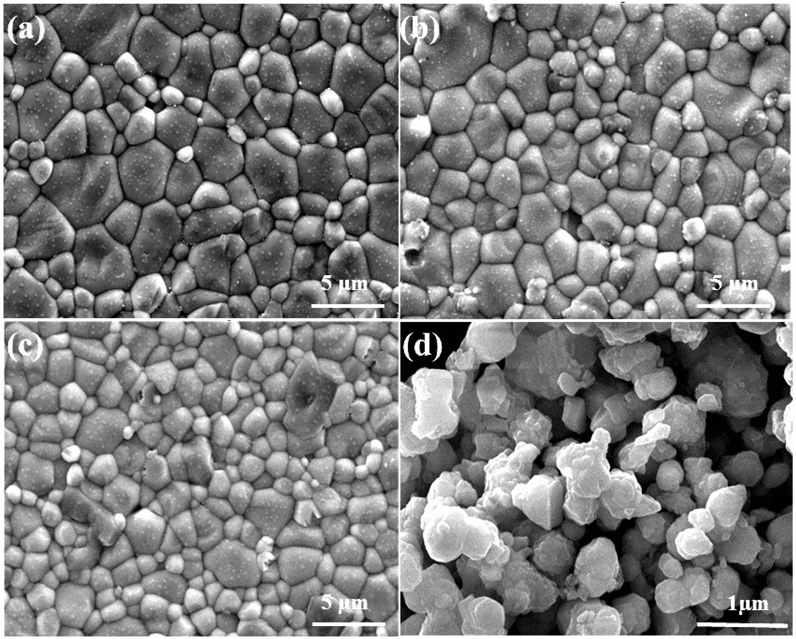
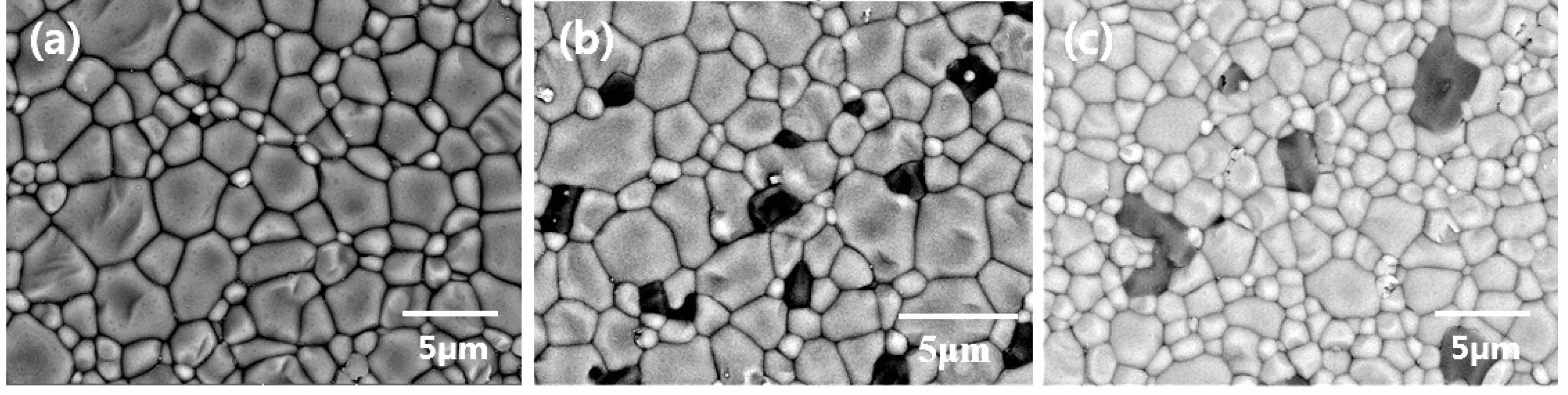
Fig. 2a-c depict surface FE-SEM images of BNT-ST-xKN specimens sintered at 1150 ℃. All samples exhibit a quite uniform and dense microstructure, confirming a high densification behavior, which ensures good electrical properties of these ceramics. The excellent sinterability can be attributed to the fine-sized particles (less than 1µm) and uniformity of the calcined powder, as shown in Fig. 2d. Sintered pellets with a relative density of over 95% prepared from the nano-sized BNT powders were also reported by Kang et al. [32]. Substitution of the KN resulted in finer grains. The average grain size of the ceramics studied here decreased from 2.2 µm for x=0 to 1.0 µm when x=0.03. This change in the BNT-ST grain size caused by the addition of KN is similar to the case of ST affecting the BNT system [18, 19, 25, 26].
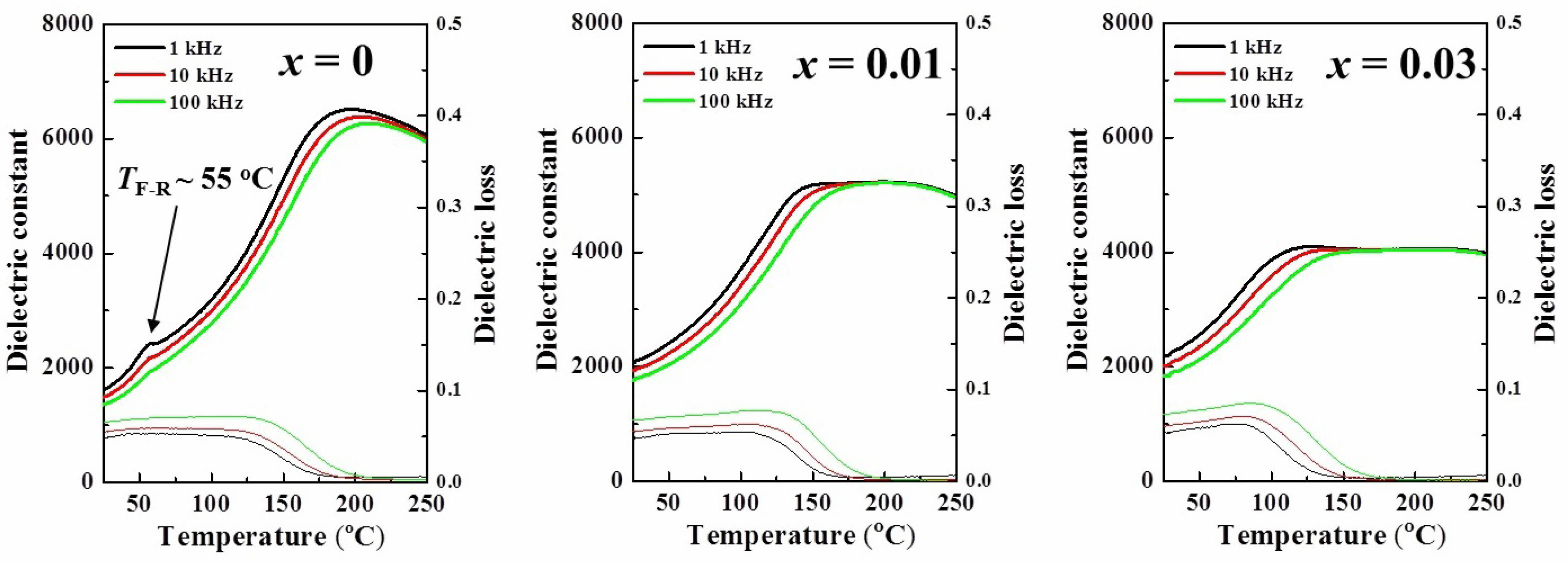
Fig. 3 presents plots of the temperature dependence (εr–T) of the relative dielectric permittivity (εr) and loss (tan δ) for BNT-ST-xKN ceramics, measured at different frequencies of 1 kHz, 10 kHz, and 100 kHz and in the temperature range of RT (25 oC)~250 oC. It is seen that all compositions exhibit a strong frequency dispersion and a broad temperature dependence of the εr peak near the maximum dielectric permittivity temperature (Tm). These phenomena imply that these ceramics can be categorized as relaxor materials. In general, the ferroelectric properties of BNT-ST-based ceramics are associated with a phase transition, known as the ferroelectric-to-relaxor (F-R) transition, where the electric-field-induced long-range order changes to a short range order [15, 33]. The occurrence of this F-R transition involves a repeating cycle of polarization and depolarization, which enables domain switching and frequency dependence [16, 18, 19]. In the εr–T dependence curve, the F-R transition temperature
(TF-R) corresponds to the peak at a low temperature, and the other anomaly at a higher temperature is related to Tm [20]. As shown in Fig. 3,upon the aforementioned addition of KN (x =0-0.03), Tm shifted toward a lower temperature (from 198 oC to 128 oC), accompanied by a decrease in εr. On the other hand, a TF-R value of around 55 oC was found for pure BNT-ST (x =0), consistent with findings reported by Lee et al. for the 0.78Bi0.5Na0.5TiO3-0.22SrTiO3 composition [34]. When x ≥ 0.01, TF-R cannot be observed in the εr–T curve, indicating that the F-R transition in such cases occurred below RT. This is clear evidence that the F-R transition was induced by the presence of KN. Numerous previous reports focusing on BNT–based relaxor materials also pointed out that the F-R transition can be induced by means of a compositional modification with various modifiers [35, 36].
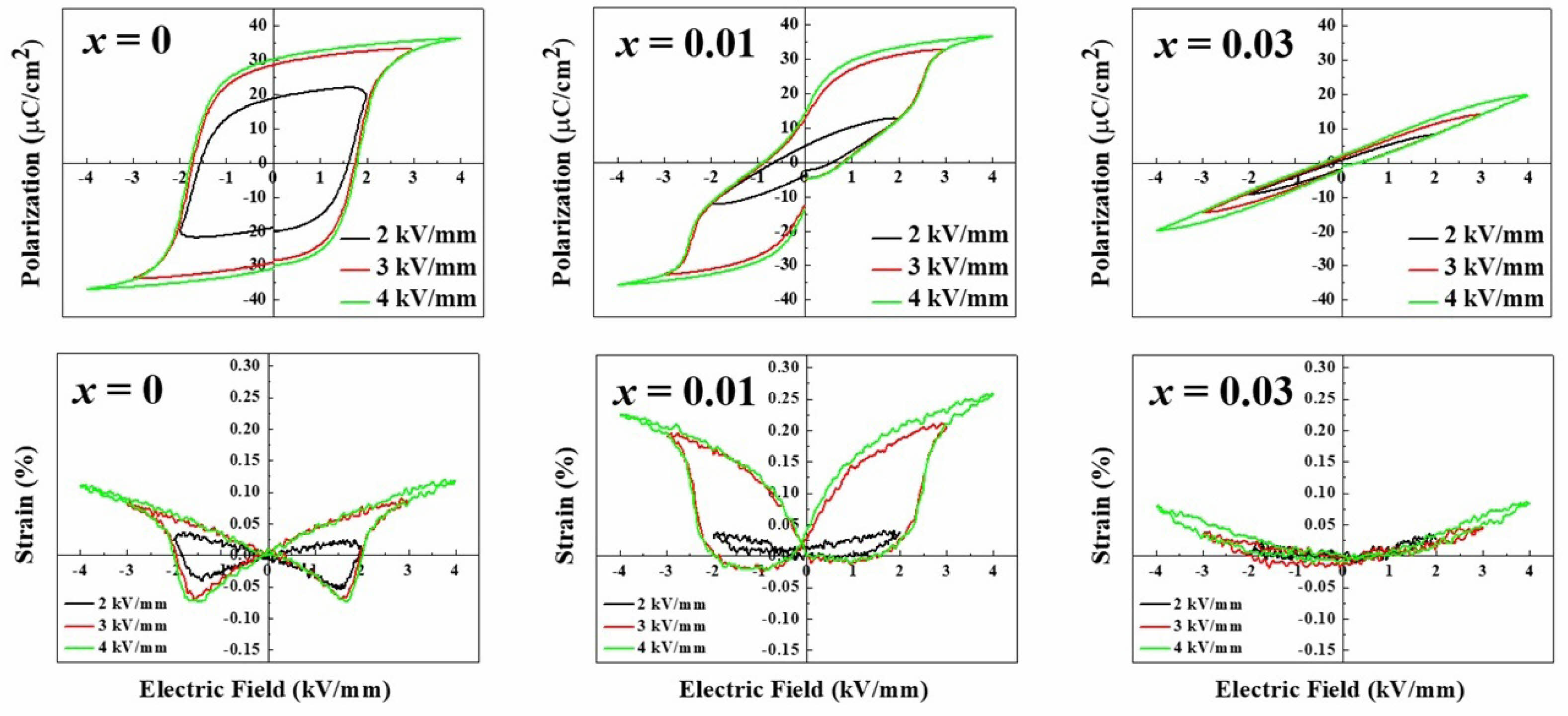
Bipolar P-E hysteresis loops and S-E strain curves of BNT-ST-xKN ceramics measured under an applied electric field in the range of 2-4 kV/mm at RT are presented in Fig. 4. Square–shaped polarization loops (Fig. 4a) together with butterfly–shaped strain curves (Fig. 4b) were revealed for pure BNT-ST (x=0). It should be noted that TF-R for pure BNT-ST is around 55 oC, meaning that it should be in a ferroelectric or a nonergodic relaxor (NER) state under this TF-R temperature. Thus, it is reasonable when this specimen possesses typical ferroelectric behavior under an applied electric field at RT. In this NER state (x=0), the S-E curve showed a large and deep negative strain (Sneg). However, in the presence of KN, Sneg was reduced and the P-E loops were pinched, being slim with a reduction in the remnant polarization (Pr) and the coercive field (EC), regardless of the strength of the applied electric field. These changes indicate that the introduction of KN weakened the ferroelectric behavior and that the ceramics were partially transformed to “non-polar” phases under a zero electric field. This result is in good agreement with the shift of TF-R to below RT, as shown in Fig. 3. Based on previous reports of BNT-based relaxor ceramics, such a weakly polar state of ceramics at RT is known as an ergodic relaxor (ER) phase [3, 16-19, 33-36]. Changes in the P-E and S-E curves here are mainly assigned to the phase transition behavior from NER to ER [37, 38], despite the decrease in the grain size shown in Fig. 2. As can be observed from Fig. 4, the maximum strain (Smax) increased and reached its highest value at x=0.01. This large strain is associated with simultaneous reductions in Pr, EC and Sneg, which is a common trade–off relationship in BNT–based relaxors [34]. When increasing the KN content further to x=0.03, however, Snegvanished in these ceramics and a flattened P-E loop was noted with sharp decreases in Pr and EC, suggesting an electrostrictive behavior.
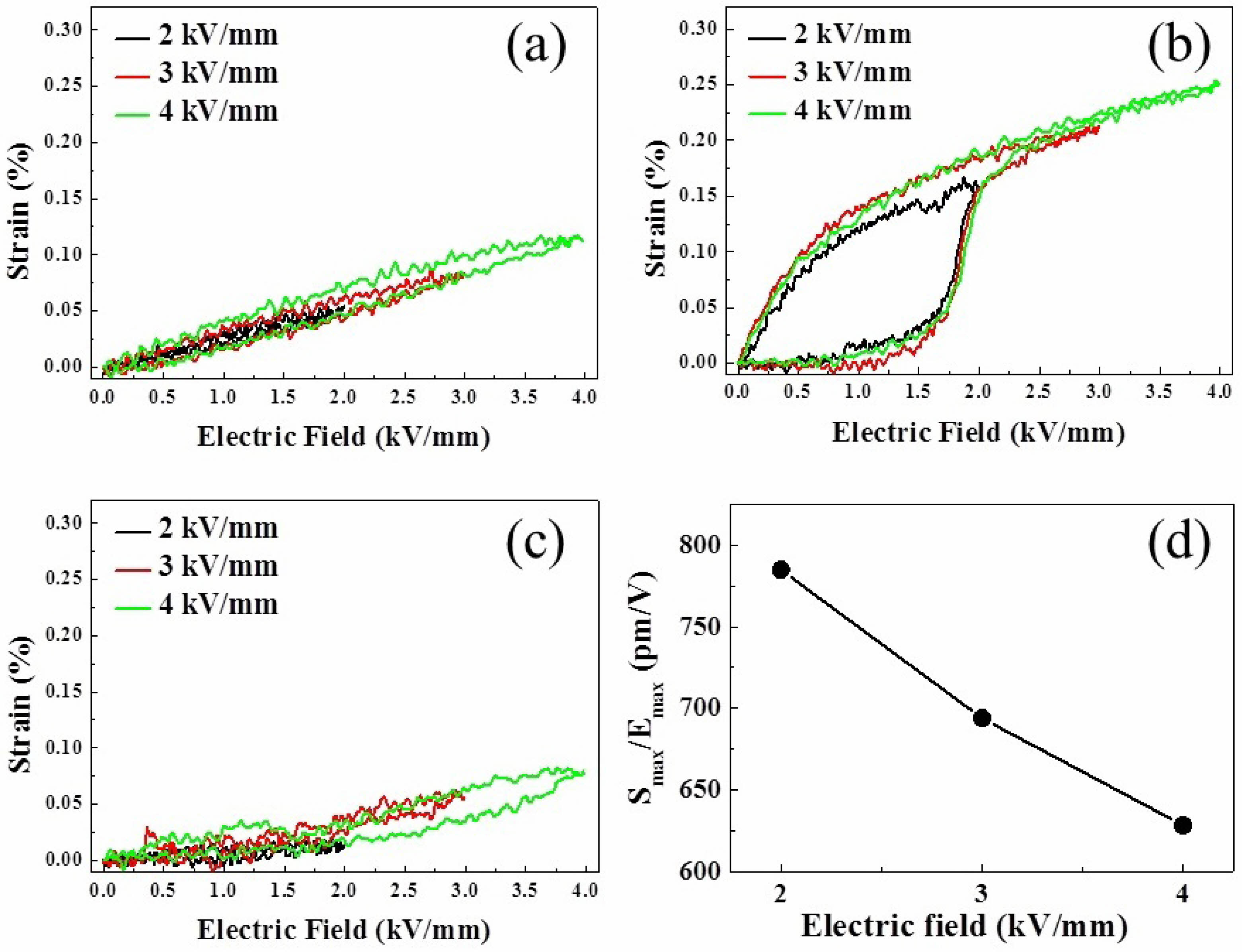
Fig. 5 shows the unipolar strain outcomes of the present ceramics measured under different electric fields (2-4 kV/mm). The strain initially increased, reaching its maximum value, and then decreased with the addition of KN, similarly to that observed for the bipolar strain (Fig. 4). An abnormally large strain (Fig. 5b) is revealed at x=0.01 regardless of the strength of the applied electric field. Notably, unipolar strain of 0.157% with a corresponding normalized strain value d33* (Smax/Emax) of 785 pm/V was achieved under an electric field of 2 kV/mm (Fig. 5d). This electro-strain is comparable to those of current commercial Pb-based compounds and ferroelectric/relaxor composites under even higher external fields [20, 22, 25, 34, 36]. Obviously, at 2 kV/mm the unipolar Smax of 0.157% is much larger than the bipolar Smax (~0.038%) in Fig. 4, but they are nearly same at 3 kV/mm (~0.216%) and 4 kV/mm (~0.251%). This behavior may be related to the difference in the poling field based on the mechanisms of the measurement modes. Given that the applied electric field for bipolar strain changes its direction periodically, the ceramic may move back to its de-poled state. In contrast, the ferroelectric domains are reoriented, and this polarized state can be continuously maintained under a unipolar field. As a result, the unipolar mode commonly requires a lower critical electric field to trigger a full response. Otherwise, the similar Smax values at 3 and 4 kV/mm mean that the applied fields are higher than the critical poling field in both of these measured modes.
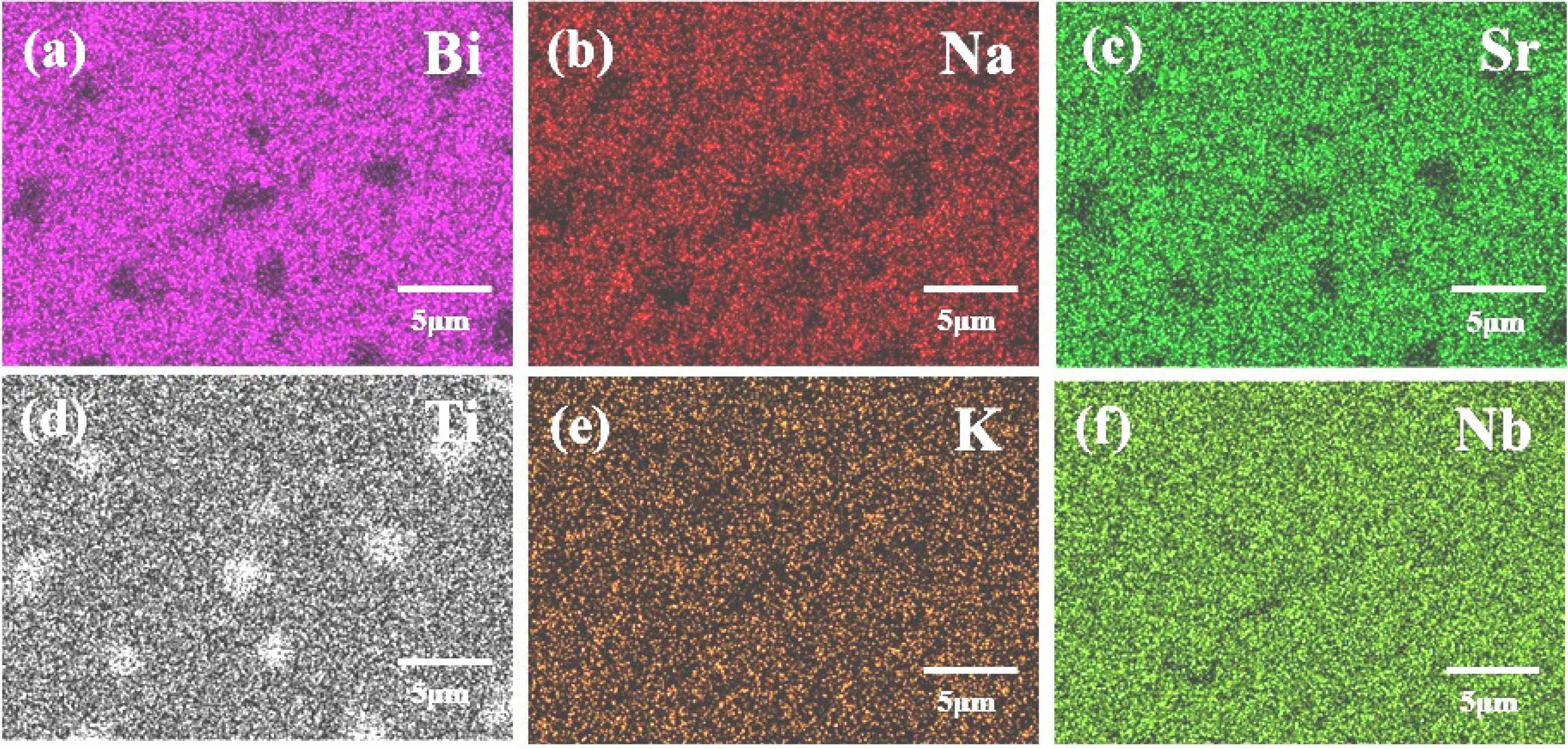
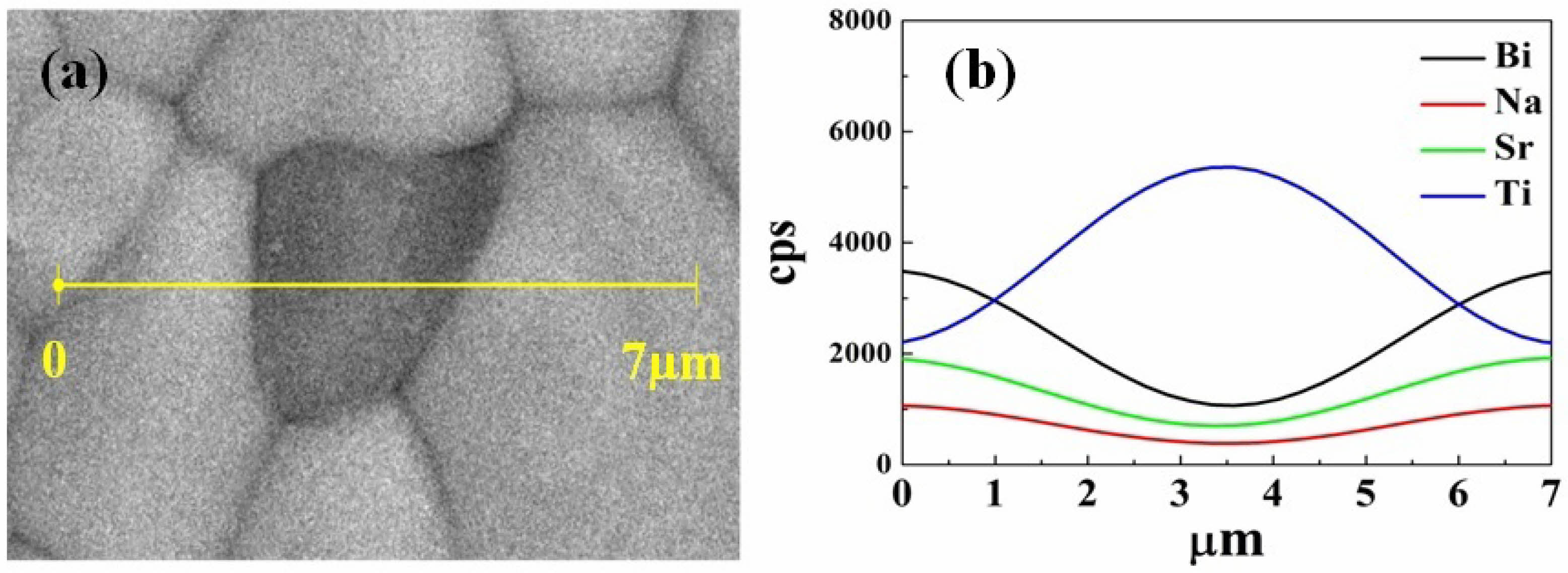
Unlike BNT-BT and BNT-BKT ceramic systems, where the coexistence of different phase structures are attributable to the enhanced piezoresponses, most researchers agree that the high strain characteristic in the BNT-ST system is associated with the F-R phase transition [3, 15, 18-20, 35]. The F-R phase transition was reported as not strictly related to changes in the lattice symmetry but rather involving a state of local chemical inhomogeneity [39-41]. Here, we examined the distribution of constituent elements on the surfaces of ceramic pellets by FE-SEM via the BSE mode and EDX mapping. Fig. 6 shows the result of BSE analyses of samples with different KN contents. There are no differences in the colors among the grains over the surface of the specimen for which x=0, as shown in Fig. 6a. In other words, all of the constituent elements are uniformly distributed within the entire ceramic material. Whereas at x=0.01, single dark-colored grains can be observed within the brightly colored grain matrix (Fig. 6b). These dark grains tend to merge into large subgroups of several grains when increasing KN further to x=0.03 (Fig. 6c). These changes indicate that the presence of KN caused a non-uniform distribution of the constituent elements (known as local chemical inhomogeneity) in the ceramics. Moreover, it was noted that the higher the content of KN, the greater the difference in the element distribution. The EDX mapping result in Fig. 7 shows that the expected elements of Bi, Na, Sr, Ti, K and Nb were detected on the BNT-ST-0.01KN sample shown in Fig. 6b. While K and Nb appear to be quite uniform over the entire area (Figs. 7e and f), Fig. 7d, however, indicates the aggregation of Ti, which results in the dark-colored grains in Fig. 6. On the other hand, Bi, Na, and Sr are present on the ceramic surface, except at the areas occupied by Ti, suggesting that these elements exist in the brightly colored grain matrix shown in Fig. 6. Fig. 8 presents a EDX line scan that was employed to investigate the elemental distribution across a dark grain in Fig. 6. As is apparent in Fig. 8, Ti mainly dominates the entire grain, with a high concentration at the center part, whereas Bi, Na and Sr are found only in small amounts near the grain boundary. These results demonstrate local separation between the A-sites (Bi, Na and Sr) and B-sites (Ti) in the perovskite BNT-ST system, which must be associated with the opposite diffusion tendencies in the solid phase. It should also be noted that the local high concentration of Ti suggests the existence of titanium oxide (TiO2), which may have formed during the sintering process. As a natural semiconductor, TiO2 can provide charges to form a local field that may further influence the distribution and/or reorientation of ferroelectric domains [42], leading to a high strain and a low driving electric field.
|
Fig. 1 (a) XRD patterns of BNT-ST-xKN (x=0.01-0.03) ceramics. (b) Enlarged XRD patterns show an unchanged pseudocubic structure regardless the increasing x. |
|
Fig. 2 SEM micrographs of the BNT-ST- xKN ceramics sintered at 1150 for 2h: (a) x=0 (b) x=0.01 (c) x=0.03. (d) calcined powder (x=0.01) after sieving |
|
Fig. 3 Temperature dependence of dielectric constant and dielectric loss of BNT-ST-xKN ceramics measured at RT and 1 kHz.. |
|
Fig. 4 Electric field induced polarization and strain of BNT-ST-xKN (x=0.01-0.03) ceramics measured at RT and 1 kHz. |
|
Fig. 5 Unipolar Electric field induced strain loops of BNT-ST-xKN: (a) x=0, (b) x=0.01 and (c) x=0.03) ceramics measured at RT and 1 kHz. (d) normalized strain values extracted from Fig. 5b. |
|
Fig. 6 BSE images observed on the surface of the BNT-ST-xKN specimen (a) x=0 (b) x=0.01 (c) x=0.03. |
|
Fig. 7 EDX mapping images of the BNT-ST-0.01KN specimen (a) Bi (b) Na (c) Sr (d) Ti (e) K (f) Nb. |
|
Fig. 8 (a) EDS line scanning on the surface of the BNT–ST–0.01KN specimen. (b) Scanned line profile. |
This study investigated the effects of KN modification on the crystal structure, microstructure, and electro-strain of lead-free BNT-ST-xKN (x =0-0.03) ceramics. The crystal structure was unchanged; however, an increase in the grain size was observed with the presence of KN. TF-R was found to decrease from 55 oC for x=0 to below room temperature for x≥ 0.01, suggesting an induced F-R transition. Notably, at x = 0.01, large unipolar-field-induced strain (Smax) of up to 0.157% with a corresponding normalized strain d33* (Smax/Emax) value of 785 pm/V were achieved at 2 kV/mm. The high strain under an ultra-low electric field was attributed to the non-uniform distribution of the constituent elements, particularly the aggregation of Ti. With the simultaneous advantages of high strain, small hysteresis, and a low driving electric field, the present ceramics are promising candidates for use in practical actuators.
This work was supported by the Electronic Component Industry Technology Research and Development (RS-2024-00419333) funded by the Ministry of Trade, Industry & Energy (MOTIE, Korea).
On behalf of all authors, the corresponding author states that there is no conflict of interest.
- 1. B. Jaffe, W.R. Cook, and H. Jaffe in “Piezoelectric ceramics” (Academic Press, London. 1971) p. 1.
-

- 2. K. Uchino, in “Piezoelectric actuators and ultrsonic motors” (Kluwer Academic Publishers, Boston, 1997).
-
- 3. W. Jo, R. Dittmer, M. Acosta, J. Zang, C. Groh, E. Sapper, K. Wang, and J. Rodel, J. Electroceram. 29[1] (2012) 71-93.
-
- 4. S.O. Leontsev and R.E. Eitel, Sci. Technol. Adv. Mater. 11[4] (2010) 044302.
-
- 5. J. Rödel, W. Jo, K.T.P. Seifert, E.-M. Anton, T. Granzow, and D. Damjanovic, J. Am. Ceram. Soc. 92[6] (2009) 1153-1177.
-
- 6. R. Jing, L. Zhang, Q. Hu, D.O. Alikin, V. Ya Shur, X. Wei, L. Zhang, G. Liu, H. Zhang, and L. Jin, J. Materiomics. 8[2] (2022) 335-346.
-
- 7. Y. Guo, M. Gu, H. Luo, Y. Liu, and R.L. Withers, Phys. Rev. B. 83[5] (2011) 054118.
-
- 8. Y. Hiruma, H. Nagata, and T. Takenaka, Jpn. J. Appl. Phys. 48[9S1] (2009) 09KC08.
-
- 9. J.H. Cho, Y.J. Ma, Y.H. Lee, M.P. Chun, and B.I. Kim, J. Ceram. Process. Res. 7[2] (2006) 91-94.
- 10. G. Song, F. Liu, F. Zhang, Z. Liu, and Y. Li, IOP Conf. Ser.: Mater. Sci. Eng. 678[1] (2019) 012140.
-
- 11. N. Sun, Y. Li, Q. Zhang, and X. Hao, J. Mater. Chem. C 6[40] (2018) 10693-10703.
-
- 12. X.-C. Zheng, G.-P. Zheng, Z. Lin, and Z.-Y. Jiang, Ceram. Int. 39[2] (2013) 1233-1240.
-
- 13. J.H. Cho, Y.H. Jeong, J.H. Nam, J.S. Yun, and Y.J. Park, Ceram. Int. 40[6] (2014) 8419-8425.
-
- 14. T.V.D. Ngoc, H.S. Han, K.J. Kim, R.A. Malik, A. Hussain, and J.S. Lee, J. Ceram. Process. Res. 13 (2012) s177-s180.
-
- 15. A. Ullah, M. Ullah, A. Ullah, A. Ullah, G. Saddiq, B. Ullah, A. Zeb, S. Ullah Jan, and I.W. Kim, J. Korean Phys. Soc. 74[6] (2019) 589-594.
-
- 16. L. Li, J. Zhang, R. Wang, M. Zheng, Y. Hou, H. Zhang, S. Zhang, and M. Zhu. J. Eur. Ceram. Soc. 39[5] (2019) 1827-1836.
-
- 17. B. Parija, T. Badapanda, and S. Panigrahi, J. Ceram. Process. Res. 16[5] (2015) 565-571.
-
- 18. M. Acosta, W. Jo, and J. Rödel, J. Am. Ceram. Soc. 97[6] (2014) 1937-1943.
-
- 19. M. Acosta, L.A. Schmitt, L.M. Luna, M.C. Scherrer, M. Brilz, K.G. Webber, M. Deluca, H.J. Kleebe, J. Rödel, and W. Donner, J. Am. Ceram. Soc. 98[11] (2015) 3405-3422.
-
- 20. X.Y. Tong, H.L. Li, J.J. Zhou, H. Liu, and J.Z. Fang, Ceram. Int. 42[14] (2016) 16153-16159.
-
- 21. A. Sasaki, T. Chiba, Y. Mamiya, and E. Otsuki, Jpn. J. Appl. Phys. 38[9S] (1999) 5564.
-
- 22. Y. Shen, H. Xie, Y. Sun, J. Xu, L. Yang, X. Pan, C. Zhou, and H. Wang, Bull. Mater. Sci. 44[2] (2021) 100.
-
- 23. B.J. Chu, J.H. Cho, Y.H. Lee, B.I. Kim, and D.R. Chen, J. Ceram. Process. Res. 3[3] (2002) 231-234.
- 24. Y. Hiruma, Y. Imai, Y. Watanabe, H. Nagata, and T. Takenaka, Appl. Phys. Lett. 92[26] (2008) 262904.
-
- 25. G. Wang, Y.H. Hong, H.T.K. Nguyen, B.W. Kim, C.W. Ahn, H.S. Han, and J.S. Lee, Sens. Actuators A: Phys. 293 (2019) 1-6.
-
- 26. T.A. Duong, M.A. Devita, H.S. Han, and J.S. Lee, Mater. Lett. 331 (2023) 133523.
-
- 27. X. Jiang, B. Wang, L. Luo, W. Li, J. Zhou, and H. Chen, J. Solid. State. Chem. 213 (2014) 72-78.
-
- 28. P. Kantha, and N. Pisitpipathsin, Integr. Ferroelectr. 187[1] (2018) 129-137.
-
- 29. X. Chen, D. Zhang, H. Liu, C. Zhou, M. Shen, P. Liu, W. Cai, H. Zhang, B. Fan, and X. Liu, Ceram. Int. 48[21] (2022) 31381-31388.
-
- 30. J. Wang, Y. Pu, G. Yang, and J. Wei, Ferroelectr. 404[1] (2010) 247-253.
-
- 31. P. Kantha, P. Raksa, M. Unruan, T. Tunkasiri, P. Jaiban, and N. Pisitpipathsin, Key. Eng. Mater. 751 (2017) 384-389.
-
- 32. D.S. Jung, H.Y. Koo, and Y.C. Kang, J. Ceram. Process. Res 11[4] (2010) 425-431.
-
- 33. K. Wang, A. Hussain, W. Jo, J. Rödel, and D.D. Viehland, J. Am. Ceram. Soc. 95[7] (2012) 2241-2247.
-
- 34. T.A. Duong, H.S. Han, Y.H. Hong, Y.S. Park, H.T. K. Nguyen, T.H. Dinh, and J.S. Lee, J. Electroceram. 41[6] (2018) 73-79.
-
- 35. C.H. Lee, H.S. Han, T.A. Duong, T.H. Dinh, C.W. Ahn, and J.S. Lee, Ceram. Int. 43[14] (2017) 11071-11077.
-
- 36. J.H. Cho, J.S. Park, S.W. Kim, Y.H. Jeong, J.S. Yun, W.I. Park, Y.W. Hong, and J.H. Paik, J. Eur. Ceram. Soc. 37[10] (2017) 3313-3318.
-
- 37. W. Zhao, R. Zuo, J. Fu, and M. Shi, J. Eur. Ceram. Soc. 34[10] (2014) 2299-2309.
-
- 38. W. Bai, D. Chen, P. Zheng, B. Shen, J. Zhai, and Z. Ji, Dalton Trans. 45[20] (2016) 8573-8586.
-
- 39. D. Viehland, S.J. Jang, L.E. Cross, and M. Wuttig, J. Appl. Phys. 68[6] (1990) 2916-2921.
-
- 40. A. Ullah, A.S. Khan, M.R. Sarker, M.J. Iqbal, H.U. Khan, V. Tirth, A. Algahtani, and A. Zaman, ACS Omega 8[13] (2023) 12372-12378.
-
- 41. J.H. Cho, S.J. Jeong, S.W. Kim, C.J. Jeon, Y.H. Jeong, J.S. Yun, Y.W. Hong, and J.H. Paik, J. Am. Ceram. Soc. 101[10] (2018) 4669-4676.
-
- 42. W. Feng, B. Luo, S. Bian, E. Tian, Z. Zhang, A. Kursumovic, J.L. MacManus−Driscoll, X. Wang, and L. Li, Nat. Commun. 13[1] (2022) 5086.
-
 This Article
-
2025; 26(5): 886-893
Published on Oct 31, 2025
- 10.36410/jcpr.2025.26.5.886
- Received on Feb 21, 2025
- Revised on Apr 17, 2025
- Accepted on Apr 28, 2025
Services
- Abstract
introduction
experimental procedure
results and discussion
conclusion
- Acknowledgements
- Conflict of Interest
- References
- Full Text PDF
Shared
Correspondence to
- Jeong Ho Cho
-
Electronic Convergence Materials Division, Korea Institute of Ceramic Engineering & Technology, Jinju-si, Gyeongsangnam-do 52851, South Korea
Tel : +82-55-792-2660 Fax: +82-55-792-2651 - E-mail: goedc@kicet.re.kr
Clean-Energy Research Institute(CRI), Hanyang University, 222, Wangsimni-ro, Seongdong-gu, Seoul, 04763, Korea
E-mail: jcpr@hanyang.ac.kr