


- High surge energy capability and deterioration stability in ZnO varistors: role of sintering and post-heat-treatment conditions
Yu-min Kima, Sung-man Kanga, Sunshin Junga, Kyoung-joo Leea, Ji-hye Kwaka and Seung-kyu Choia,*
aElectrical Environment Research Center, Korea Electrotechnology Research Institute, Changwon 51543, Republic of Korea
This article is an open access article distributed under the terms of the Creative Commons Attribution Non-Commercial License (http://creativecommons.org/licenses/by-nc/4.0) which permits unrestricted non-commercial use, distribution, and reproduction in any medium, provided the original work is properly cited.
This study investigates a ZnO varistor exhibiting both high energy-handling capability and exceptional stability under high-temperature conditions. The results indicate that the sintering temperature and subsequent post-heat-treatment significantly affect the varistor's energy capacity and resistance to degradation. A systematic investigation of the microstructural and phase transformations induced by varying thermal processing conditions revealed that specimens sintered at 1200 °C and post-annealed at 600–800 °C achieved optimal performance, primarily due to grain boundary stabilization and the formation of beneficial intergranular phases.
Keywords: ZnO varistor, Post-annealing, Bismuth oxide, Energy capability, Electrical degradation.
ZnO varistors operate as nonlinear resistive devices, where electrical conduction in the pre-breakdown region is thermally activated and highly sensitive to the applied DC voltage [1-3]. In this regime, the conduction mechanism is primarily governed by thermionic emission, as well as defect-related processes occurring at grain boundaries. Under continuous electrical stress, performance degradation is often linked to an increase in resistive leakage current, which may ultimately result in thermal runaway. Accordingly, effective suppression of leakage current is essential for enhancing varistor stability and prolonging operational lifetime [4, 5].
Extensive research has emphasized the critical role of intergranular Bi₂O₃ phases in blocking charge transport and maintaining nonlinear behavior. In particular, the β- and δ-phases of Bi₂O₃ are known for their high ionic conductivity, which significantly contributes to energy-handling performance in ZnO-based systems [6, 7]. However, these beneficial phases are highly sensitive to thermal processing conditions, and volatilization of Bi₂O₃ at elevated temperatures can severely degrade both the electrical and thermal stability of the varistor.
Therefore, optimizing post-sintering annealing conditions to stabilize the β- and δ-phases without inducing excessive grain growth or Bi loss is crucial. In this study, we propose a strategy to simultaneously achieve high energy capability and superior thermal degradation resistance by carefully tailoring the post-heat-treatment temperature after primary sintering. Through a systematic investigation combining microstructural analysis and electrical characterization, we demonstrate that post-annealing at 600–800 °C following sintering at 1200 °C enables the formation of stable intergranular phases, thereby maximizing varistor performance under severe electrical stress.
Materials and Preparation
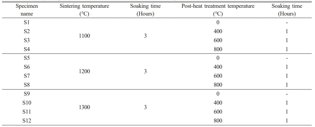
Samples were prepared with the composition: ZnO + 1 mol% Bi2O3 + 1 mol% Sb2O3 + 0.2 mol% Al2O3 + 0.4 mol% NiO + 0.4 mol% MnO. The role of Al₂O₃ doping in ZnO-based varistor composition has been previously investigated in terms of microstructure and nonlinearity enhancement [8]. In this study, a modified composition containing 0.2 mol% Al₂O₃ was adopted. The slurry was prepared using wet ball milling for 24 h with ZrO₂ balls at 180 rpm and a ball-to-powder weight ratio of 10:1. Granules were obtained via hot-air drying, followed by uniaxial pressing (13 Bar, 10 s) into square pellets (40 × 40 × 10 mm). Green bodies were sintered at 1100–1300 °C (3 h, air) with natural cooling, followed post-heat-treatment processes were performed under the conditions shown in Table 1 below. A silver electrode (39×39 mm) was formed on the sintered body using the screen-printing method. Next, the microstructure of the specimens was observed via field emission scanning electron microscopy (S-4800, Hitachi, Japan) with energy-dispersive X-ray. X-ray diffraction (X-pert PRO-MPD, Philips, Netherlands) was used to identify the phases of the sintered ZnO varistors, and X-ray fluorescence (ZSX Primus, Rigaku, Japan) was used for the quantitative analysis.
Electrical Measurements
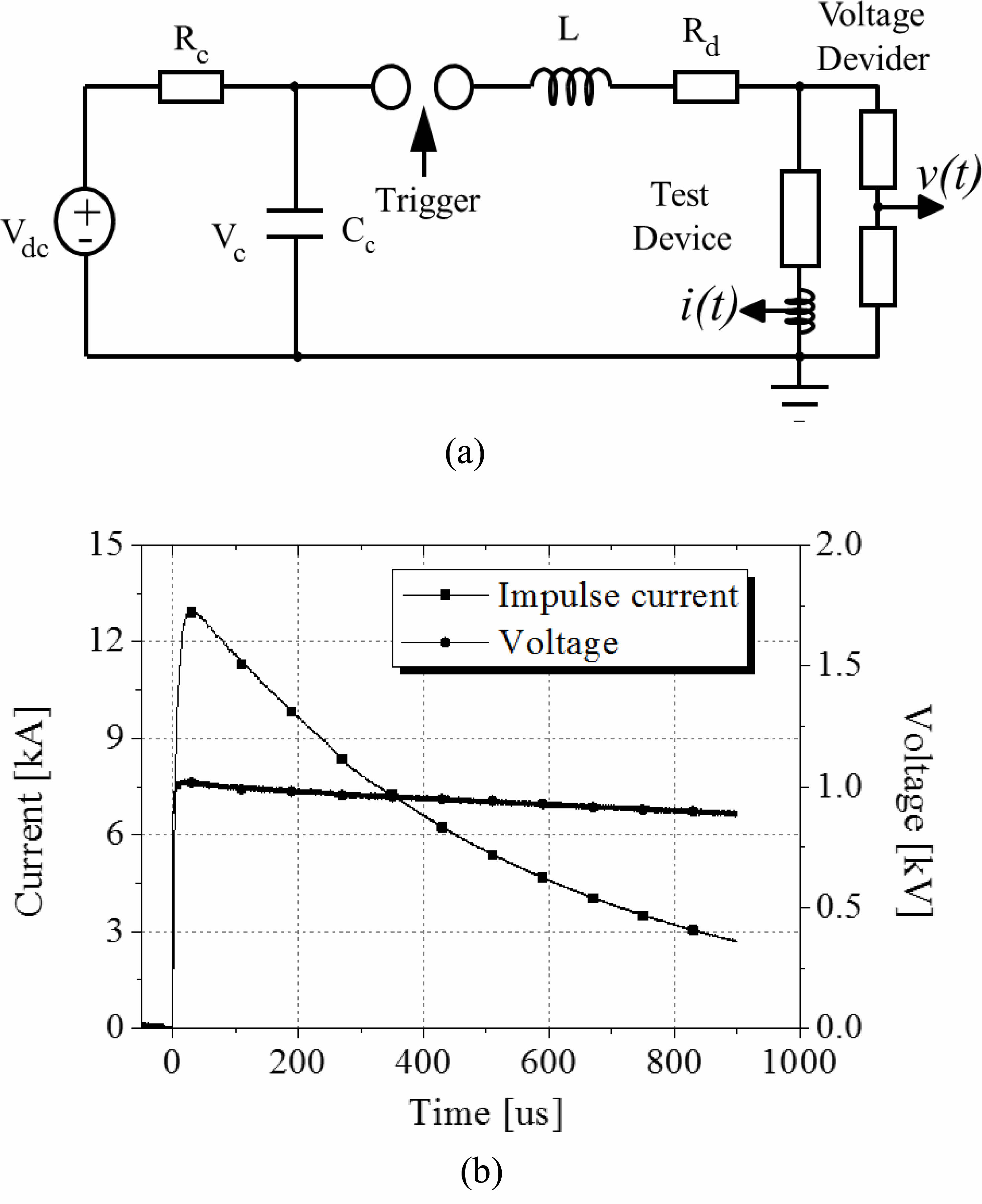
Energy capability was measured using a lightning impulse current generator (KERI-ICG-400kA, Korea Electrotechnology Research Institute, South Korea). The applied waveform was a 10/350 µs standard impulse with a peak current of 12.5 kA, as shown in the schematic and waveform in Fig. 1. The impulse current was monitored using a Pearson model 1423 current sensor (1.2 MHz bandwidth, DC to peak), while the corresponding voltage was measured with a Tektronix P6015 high-voltage probe (70 MHz bandwidth, DC to peak). The captured waveforms were recorded on a TDS3032 digital storage oscilloscope (Tektronix, USA) with 300 MHz bandwidth and 2.5 Gs/s sampling rate.
The test was conducted in accordance with the IEC 61643-11 standard [9], specifically aligning with the Class I surge protective device (SPD) testing protocol. As described in Clause 8.3.4.4 of the standard, the procedure involves applying single current impulses up to Iₙ to assess the thermal and electrical robustness of the device under test. In our study, each varistor sample was subjected to a single high-energy 10/350 µs impulse to evaluate whether catastrophic failure or a more than 10% variation in varistor voltage occurred. This test was not intended to evaluate cyclic endurance, but rather to determine the maximum energy-handling capability under simulated lightning surge conditions.
To ensure reproducibility, five specimens were tested for each condition, and the maximum withstand energy was reported. No post-pulse degradation or re-ignition was observed, confirming that the impulse energy capacity can be reliably verified using this one-shot destructive evaluation method. This approach reflects the intent of IEC 61643-11 for validating varistor components in high-energy SPD applications.
The high-temperature accelerated deterioration test was conducted using a high-temperature accelerated deterioration testing apparatus (KERI-HTADT-1kV, KERI, South Korea), where the maximum continuous operating voltage (MCOV, DC) was applied at 85 °C to measure the resistance component of leakage current for 100 hours.
|
Fig. 1 (a) Schematic diagram of the impulse current generator and (b) the applied waveform (10/350 µs, 12.5 kA). |
|
Table 1 Sintering and post-heat-treatment conditions for ZnO varistor specimens. |
Microstructure Observation
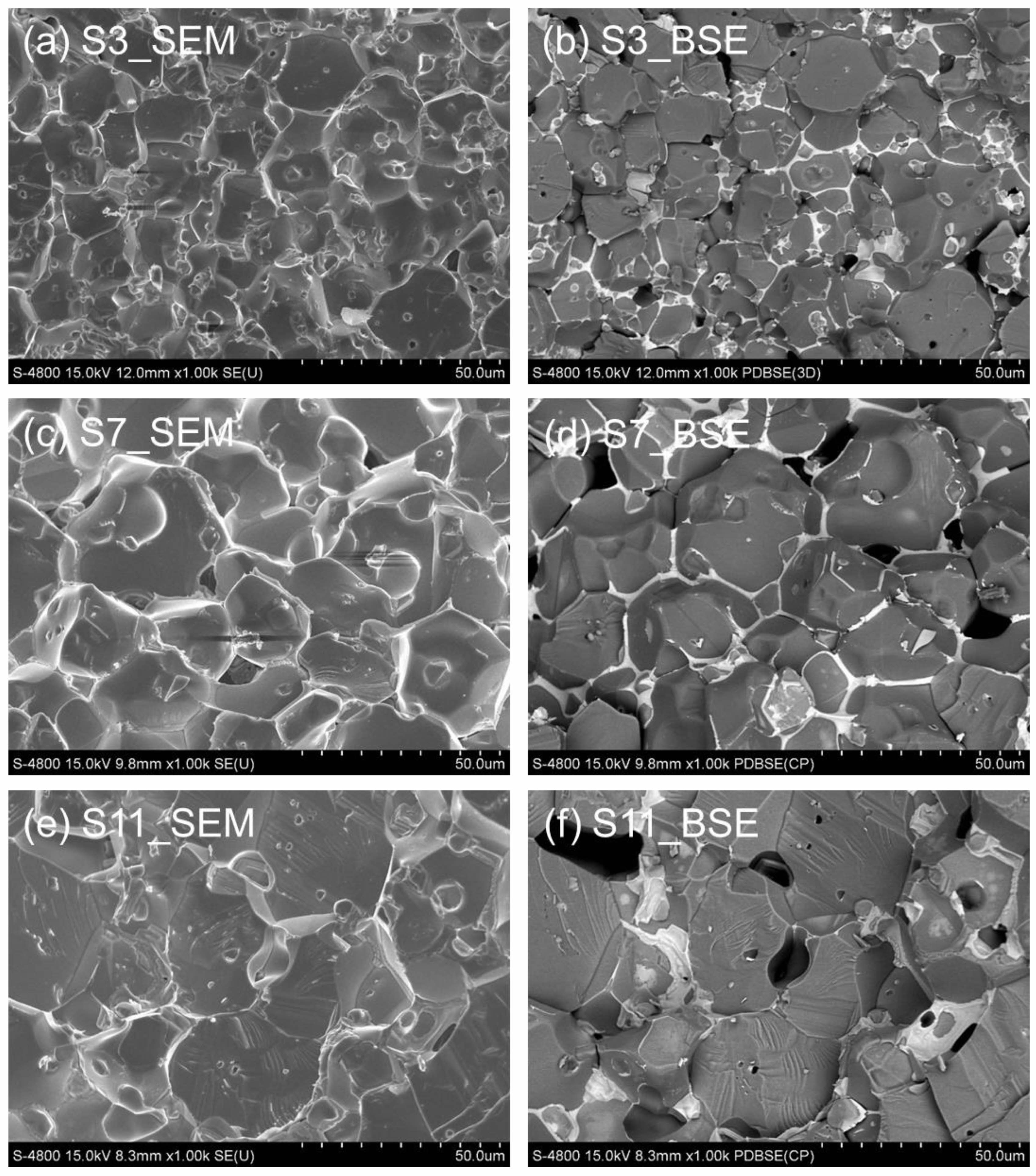
As shown in Fig. 2, the average ZnO grain size increased significantly with rising sintering temperature: approximately 8–10 µm for S3 (1100 °C), 18–20 µm for S7 (1200 °C), and 23–25 µm for S11 (1300 °C), as measured by the linear intercept method. This grain growth directly influences the varistor voltage, which is inversely related to the number of grains per unit thickness. The BSE images reveal increased contrast and phase separation in S7, indicating the presence of spinel phases (e.g., ZnSb₂O₆) at the grain boundaries, which help suppress abnormal grain growth. In contrast, the S11 sample exhibits irregularly large grains and less-defined boundary phases, likely due to bismuth volatilization, which may compromise microstructural stability at elevated temperatures [10, 11].
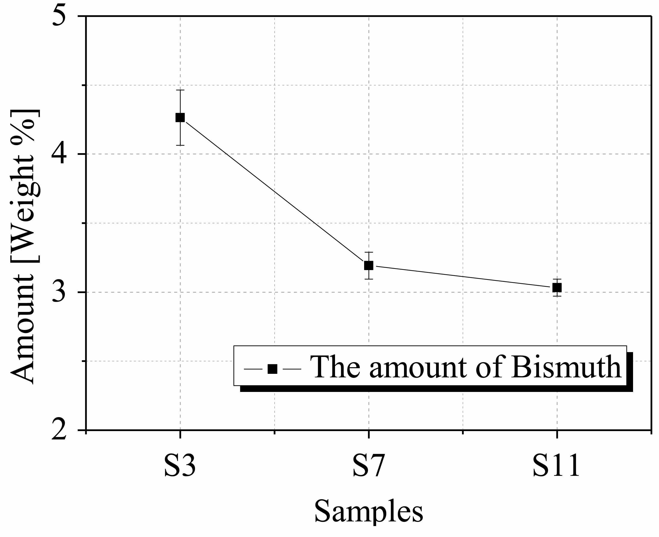
To quantify the bismuth distribution, XRF analysis was conducted and the results are shown in Fig. 3. The bismuth content decreased significantly from S3 to S7, then slightly from S7 to S11, suggesting progressive volatilization of Bi₂O₃ with increasing sintering temperature [12].
Phase Identification and Energy Capability
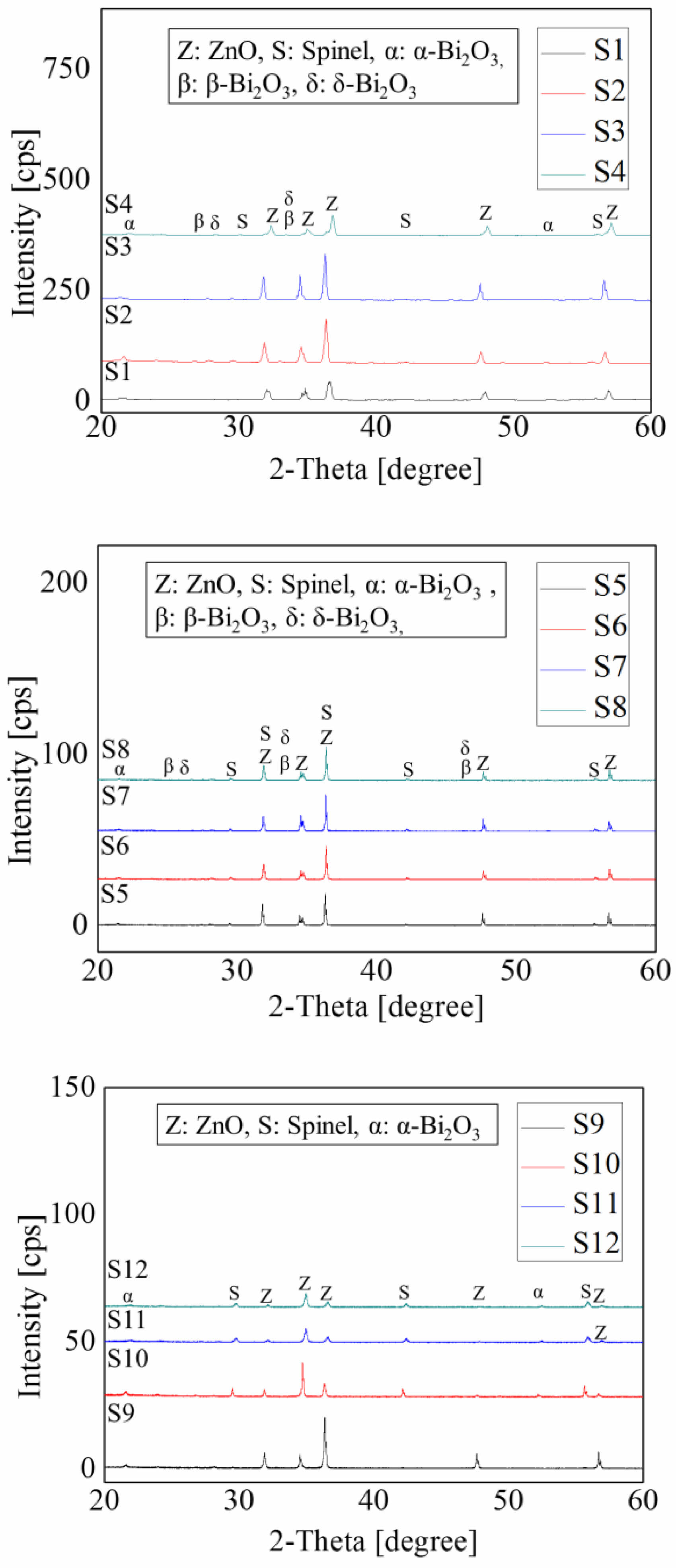
XRD analysis results are presented in Fig. 4. Distinct β- and δ-Bi₂O₃ phases were identified in samples sintered at 1100 °C (S3, S4) and 1200 °C (S7, S8), which are known to enhance ionic conductivity. However, in the 1300 °C-sintered samples (S11, S12), the β and δ phases disappeared, and only α-Bi₂O₃ remained, indicating volatilization of bismuth oxide at elevated temperatures. Peak indexing matched standard ICDD files (#01-072-0404 for β-Bi₂O₃). The absence of low-angle peaks at 2θ ~27° and 30° confirmed the loss of these polymorphs. SEM images (Fig. 2) show a decrease in grain boundary contrast in S11, correlating with reduced Bi retention. Quantitative XRF results support this trend.
The appearance of shifted peaks in S4 is attributed to the substitutional incorporation of Mn and Ni ions into the ZnO lattice. Additionally, the variation in spinel phase intensity across samples suggests that spinel formation is influenced by both sintering conditions and dopant concentrations [13].
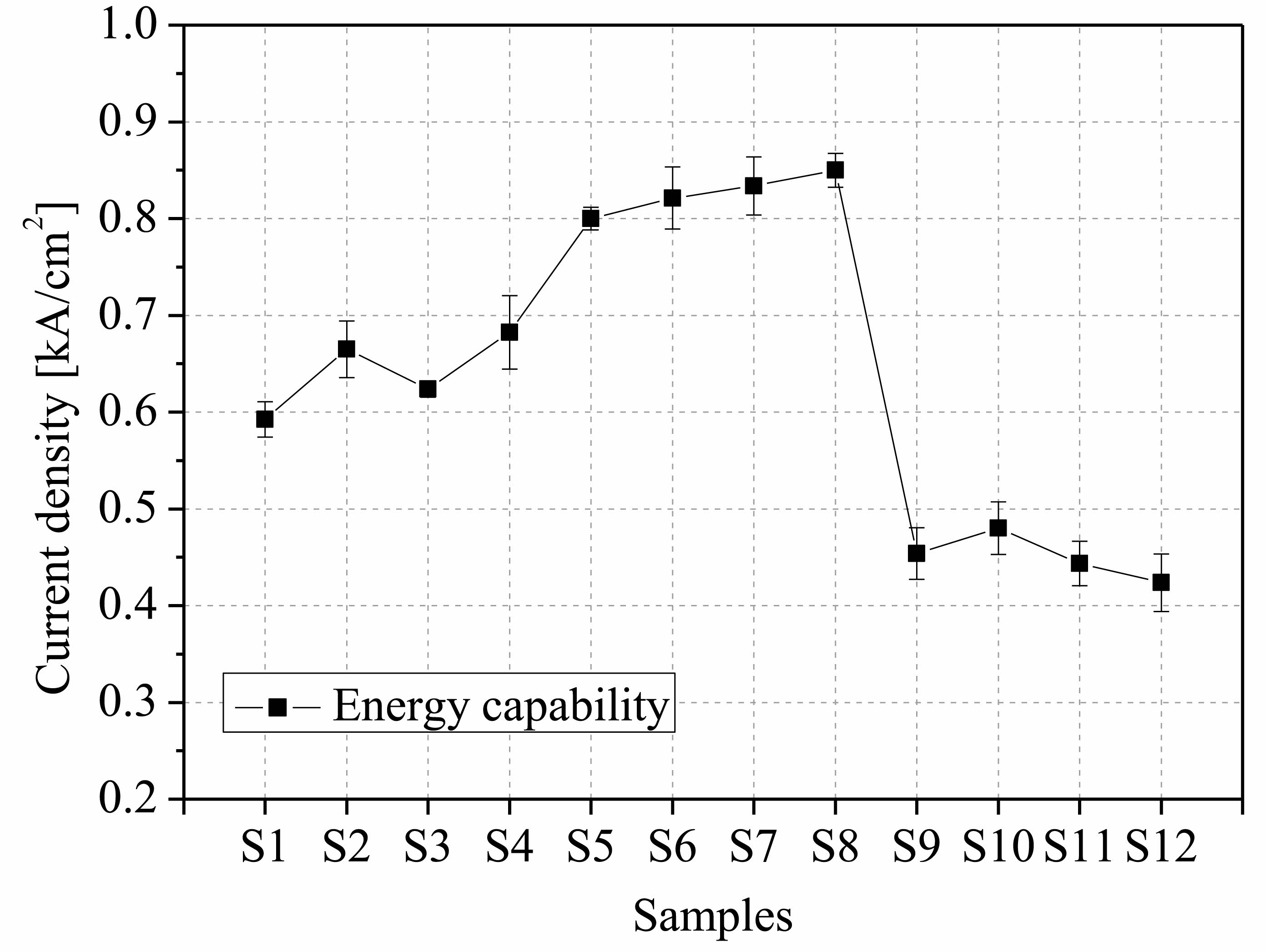
Energy capability was tested using a single 12.5 kA, 10/350 μs impulse. The failure criterion was defined as catastrophic fracture or a >10% increase in varistor voltage. Each data point represents the average of five samples with standard deviation shown as error bars in Fig. 5. Samples sintered at 1200 °C and annealed at 600–800 °C (S7, S8) ddemonstrated the highest current density of 0.86 ± 0.03 kA/cm². In contrast, those sintered at 1300 °C (S9–S12) showed a significant drop to below 0.5 kA/cm², likely due to volatilization of Bi₂O₃ and the subsequent disappearance of β and δ phases with high ionic conductivity. Although the 1100 °C samples (S1–S4) retained these bismuth phases, their grain boundaries appeared to be excessively enriched with amorphous Bi₂O₃, which may have limited effective ionic transport. These results align with the phase composition and microstructure observations from XRD, SEM/BSE, and XRF analyses.
Thermal Stress and Electrical Stability
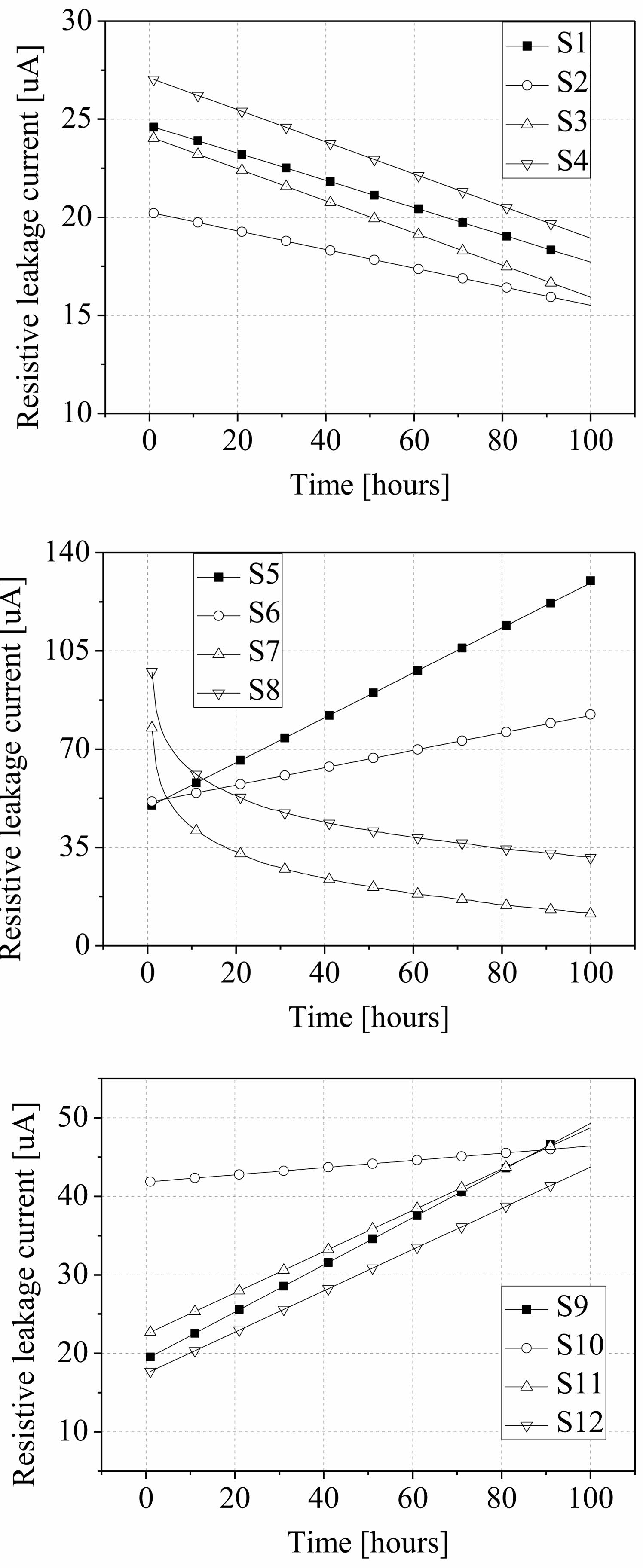
As shown in Fig. 6, the leakage current behavior of samples sintered at 1200 °C varied significantly depending on the post-heat-treatment condition. S5 (no annealing) and S6 (400 °C) exhibited a continuous increase in resistive leakage current over 100 hours, reaching up to ~135 μA and ~85 μA respectively, likely due to Zn diffusion into the depletion layer and insufficient grain boundary stabilization [2]. In contrast, S7 and S8 (600 °C and 800 °C annealed) showed a steady decrease in leakage current, suggesting that oxygen adsorption played a critical role in stabilizing the depletion layers and suppressing interstitial Zn migration [14]. Meanwhile, the 1300 °C-sintered samples (S9–S12) exhibited increased leakage current under all post-treatment conditions, likely due to Bi₂O₃ volatilization, which hindered the formation of a resistive and stable intergranular phase [15-17].
|
Fig. 2 SEM images of the microstructure at different sintering temperatures. |
|
Fig. 3 Amount of Bi element determined via XRF. |
|
Fig. 4 XRD patterns under different sintering and post-heattreatment temperature conditions. |
|
Fig. 5 Test results of energy capability under a 10/350 µs waveform. |
|
Fig. 6 Leakage current behavior under high-temperature accelerated stress (85 °C for 100 h) at different post-heattreatment conditions. |
Post-annealing at 600–800 °C following sintering at 1200 °C led to the development of ZnO varistors exhibiting both high energy-handling capability (above 0.85 kA/cm²) and excellent thermal stability. These enhancements are attributed to the formation of β- and δ-Bi₂O₃ phases, which promoted ionic conduction, and to the stabilization of grain boundaries through effective oxygen adsorption. This study confirms that careful optimization of sintering and post-annealing conditions is essential for ensuring the long-term reliability and performance of ZnO-based varistor.
This work was supported by a Korea Institute of Energy Technology Evaluation and Planning (KETEP) grant funded by the Korean government (MOTIE) (20213030020290, Development of a lightning protection platform for large-scale offshore wind farms).
- 1. F. Greuter and G. Blatter, Semicond. Sci. Technol. 5[1] (1990) 111-137.
-

- 2. T.K. Gupta and W.G. Carlson, J. Mater. Sci. 20[10] (1985) 3487-3500.
-
- 3. A. Iga, M. Matsuoka, and T. Masuyama, Jpn. J. Appl. Phys. 15[6] (1976) 1161-1167.
-
- 4. J. He, C. Cheng, and J. Hu, AIP Adv. 6[3] (2016) 030701.
-
- 5. M. Mizuno, M. Hayashi, and K. Mitani, IEEE Trans. Power Appar. Syst. PAS-100[5] (1981) 2664-2671.
-
- 6. S.K. Choi, H.H. Jung, and S.M. Kang, J. Ceram. Soc. Jpn. 25[5] (2005) 1675-1680.
- 7. H.A. Harwig and A.G. Gerards, J. Solid State Chem. 26[3] (1978) 265-274.
-
- 8. N.R. Noori, R.S. Mamoory, A. Mehdikhani, and A.M. Hadian, J. Ceram. Process. Res. 9[2] (2008) 107-110.
-
- 9. International standard, IEC 61643-11, “Low-voltage surge protective devices, Part 11: Surge protective devices connected to low-voltage power systems, Requirements and test methods”, Edition 1.0 (2011) 03.
- 10. E. Olsson and G.L. Dunlop, J. Appl. Phys. 66[9] (1989) 4317-4325.
-
- 11. S. Lee, C.K. Sohn, A. Djafar, M.T. Cho, and J.R. Yoon, J. Ceram. Process. Res. 20[2] (2019) 164-168.
-
- 12. M. Peiteado, M.A. de la Rubia, M.J. Velasco, F.J. Valle, and A.C. Caballero, J. Eur. Ceram. Soc. 25[9] (2005) 1675-1680.
-
- 13. E. Olsson, L.K.L. Falk, G.L. Dunlop, and R. Österlund, J. Mater. Sci. 20[11] (1985) 4271-4278.
-
- 14. M.A. Ramírez, A.Z. Simões, P.R. Bueno, M.A. Márquez, M.O. Orlandi, and J.A. Varela, J. Mater. Sci. 41[19] (2006) 6221-6227.
-
- 15. M. Peiteado, J.F. Fernandez, and A.C. Caballero, J. Eur. Ceram. Soc. 27[13-15] (2007) 3867-3872.
-
- 16. W. Mielcarek, Ceram. Int. 39[7] (2013) 8219-8226.
-
- 17. H. Cerva and M. Russwurm, J. Am. Ceram. Soc. 71[7] (1988) 522-530.
-
 This Article
-
2025; 26(3): 507-511
Published on Jun 30, 2025
- 10.36410/jcpr.2025.26.3.507
- Received on May 1, 2025
- Revised on Jun 10, 2025
- Accepted on Jun 11, 2025
Services
- Abstract
introduction
experimental procedure
results and discussion
conclusions
- Acknowledgements
- References
- Full Text PDF
Shared
Correspondence to
- Seung-kyu Choi
-
Electrical Environment Research Center, Korea Electrotechnology Research Institute, Changwon 51543, Republic of Korea
Tel : +82 552802440 Fax: +82 552801329 - E-mail: keri87@keri.re.kr
Clean-Energy Research Institute(CRI), Hanyang University, 222, Wangsimni-ro, Seongdong-gu, Seoul, 04763, Korea
E-mail: jcpr@hanyang.ac.kr