


- Electrocaloric effect of K(Ta,Nb)O3/BaTiO3 multilayer thin films prepared by sol-gel method
Byeong-Jun Parka, Jeong-Eun Lima, Ji-Su Yuka, Sam-Haeng Leea,b, Myung-Gyu Leea,b, Joo-Seok Parkb and Sung-Gap Leea,*
aDept. of Materials Engineering and Convergence Technology, RIGET, Gyeongsang National University, Jinju 52828, Korea
bBusiness Support Division, Korea Institute of Ceramic Engineering and Technology, Jinju 52851, KoreaThis article is an open access article distributed under the terms of the Creative Commons Attribution Non-Commercial License (http://creativecommons.org/licenses/by-nc/4.0) which permits unrestricted non-commercial use, distribution, and reproduction in any medium, provided the original work is properly cited.
KTN/BT multilayer films were fabricated using the sol-gel method and the spin coating method. The average thickness of the single-coated film was about 62 to 67 nm and the average grain size was about 92 to 95 nm. TEM analysis made it possible to observe a clear image difference between the KTN layer and BT layer due to the difference in composition and crystal structure. As the number of coatings increased, the dielectric constant increased and the Curie temperature increased. The 6-layer KTN/BT multilayer film exhibited the highest dielectric constant of about 2530 at a transition temperature of 26 °C. The 6-layer KTN/BT multilayer films showed a remanent polarization and a coercive field of 9.2 μC/cm2 and 91 kV/cm, respectively, at around room temperature. The ΔT and ΔT/ΔE of the 5-layer KTN/BT multilayer film with an applied electric field of 150 kV/cm were 0.72 K and 4.8 mK·cm/kV, respectively, at around room temperature.
Keywords: K(Ta,Nb)O3/BaTiO3, Multilayer thin films, Electrocaloric effect, Structural properties, Electrical properties.
Chloro-fluoro-carbon (CFC, Freon) and hydro-chloro-fluoro-carbon (HCFC) gases are widely used as refrigerant materials for various home and industrial electronics such as refrigerators, chillers and air conditioners. However, due to environmental problems, hydro-fluoro-olefins (HFOs) have recently been used as next-generation refrigerant materials, but they have low performance, difficulty in miniaturization and a high price [1, 2]. In general, thermoelectric (TE) effects and electrocaloric (EC) effects are used for cooling materials of small electronic devices and semiconductor components. However, TE materials have high power consumption due to their low energy conversion efficiency. EC effect uses entropy change and temperature change as the arrangement of the electric dipoles changes when an electric field is applied to a ferroelectric material, and reversible temperature changes occur via the applied electric field or stress [3]. Since the EC effect can be manufactured in micro electronic devices and it has high efficiency, many studies recently have been conducted for their application as cooling materials. Since the EC effect is the largest near the Curie temperature (Tc), ferroelectric materials with a phase transition temperature near room temperature are required in order to be practical [4]. Many researchers have conducted studies to control the phase transition temperature and improve the electrical properties of ferroelectric Pb(Zr,Ti)O3 or BaTiO3 ceramics [5, 6]. In 2006, A. S. Mischenko et al., observed a giant EC effect (ΔT) in PZT(95/5) films near the Curie temperature of 242 oC [7]. However, due to the high Curie temperature, it is difficult to put it into practical applications, and in this study, KTN/BT multilayer thin films were fabricated to obtain EC devices that can operate at room temperature. This paper described the EC effects of KTN/BT multilayer thin films fabricated using lead-free K(Ta,Nb)O3(KTN) and BaTiO3(BT) thin films that exhibit excellent ferroelectric, piezoelectric, and nonlinear electro-optical properties. KTN exhibits control of phase transition temperature and various structural and electrical characteristics depending on the composition ratio of Ta and Nb [7]. To obtain good electrocaloric properties near room temperature, we attempted to increase the polarization by forming an interfacial polarization due to the spatial charge distribution at the interface by alternately stacking ferroelectric BT (Tc = 130 oC) and K(Ta0.65Nb0.35)O3 (Tc = 0 oC) films with different transition temperature and structural properties. To consider the possibility of application as a cooling device that can operate at room temperature, we measured the structural and electrical properties of KTN/BT multilayer films.
K(Ta0.65Nb0.35)O3 precursor solutions were prepared from C2H3KO2, C10H25TaO5 and C10H25NbO5 as the raw materials and 2-methoxyethanol as the solvent using the sol-gel method. Precursor solution synthesis was carried out in a dry N2 atmosphere to prevent reaction with the moisture in the air. BaTiO3 precursor solutions were prepared from (CH3COO)2Ba and Ti[OCH(CH3)2]4 as the raw materials and 2-methoxyethanol and acetic acid as the solvents. The synthesis processes of KTN and BT precursor solutions were carried out in the same way as in previous experiments [8, 9], and the precursor solutions were aged for 24 hours before use. KTN coating solution was coated on the Pt(111)/Ti/SiO2/Si substrates using a spinner operated at 3000 rpm for 30 s, dried at 200 °C for 5 min and annealed at 400 °C for 10 min. Then BT coating solution was spin-coated and dried/annealed on the KTN film under the same conditions to form the second layer. A variety of KTN/BT multilayer thin films were fabricated by coating 3 to 6 times. Then they were sintered at 750 °C for 1 h. The structural properties were observed using X-ray diffraction (XRD), scanning electron microscopy (SEM), and transmission electron microcopy (TEM). For electrical measurements, Pt-upper electrode with a diameter of 500 μm was deposited on the film by dc sputtering method. Dielectric properties were measured using an LCR meter (PM-6036, Fluke) in the temperature range of -150 °C to 40 °C. P-E hysteresis loops were observed using a Ferroelectric Tester (RT-66B, Radiant Tech. Inc. USA) by applying a sine wave of 10 Hz frequency, and the applied voltage was up to ±10 V, which is the maximum built-in drive voltage of the measuring instrument.
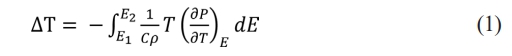
Fig. 1 shows the XRD patterns of the KTN/BT multilayer thin films. The XRD patterns of KTN/BT multilayer films showed relatively wide FWHM values, and no peaks of the BT and KTN phases could be observed. This is because the positions of the XRD peaks of BT [10] and KTN [11] are very similar. The XRD peak index was the peaks of the top-coated film on the KTN/BT multilayer films. Pyrochlore phases were observed in the 3- and 4-times coated films, but the 5-times and more coated films showed polycrystalline XRD patterns without pyrochlore phases and with high intensities. This is considered to be because, as the number of coatings increases, the stress with the substrate decreases and the crystallinity increases due to the lower KTN or BT layers acting as nucleation sites for the formation of the upper layers [12].
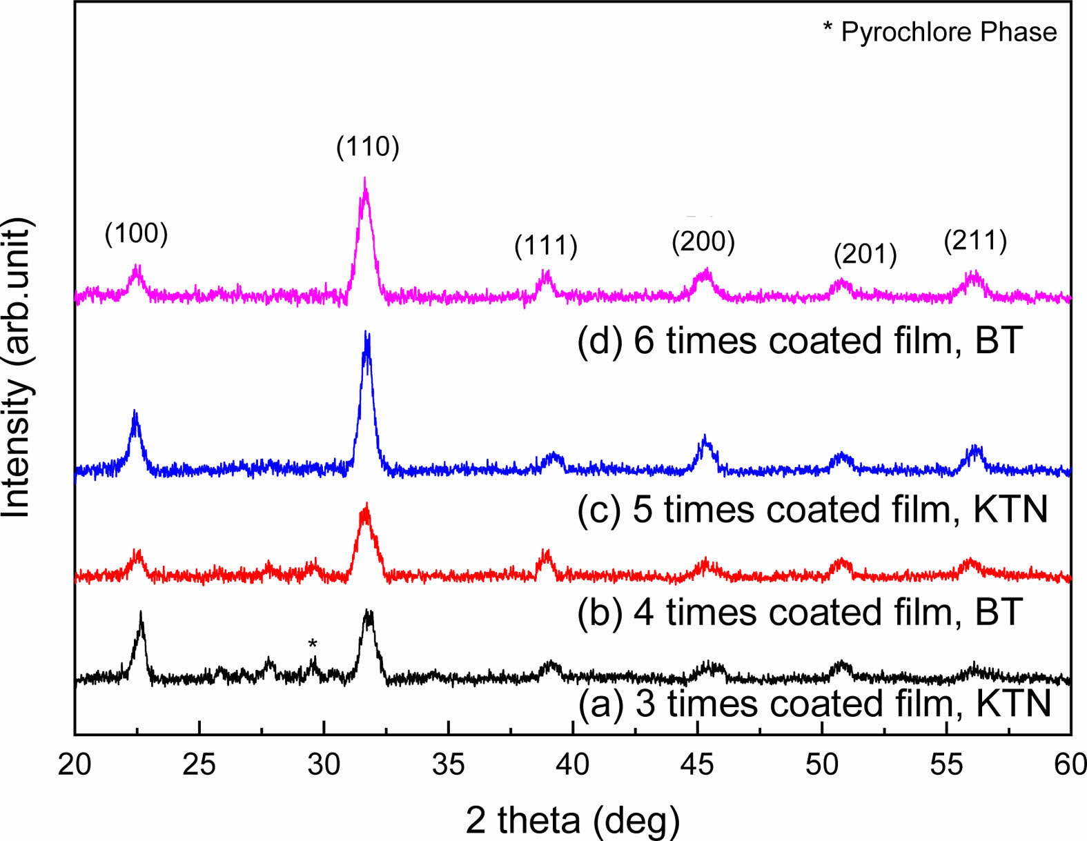
Fig. 2 shows surface and cross-sectional microstructures of the KTN/BT multilayer thin films. All films showed a uniform and dense microstructure with an average grain size of about 92 to 95 nm. This is thought to be due to the fact that when KTN and BT, which have different crystal structures and sintering temperatures, are alternately stacked and sintered, the lower layer acts as a seeding layer for the crystallization of the upper layer [13]. The thickness of the films increased from 195 nm to 397 nm as the number of coatings increased from 3 to 6 times, and the thickness of films coated once was approximately 62 to 67 nm. The pyrochlore phase observed in the 3- and 4-times coated thin films could not be observed in the microstructure.
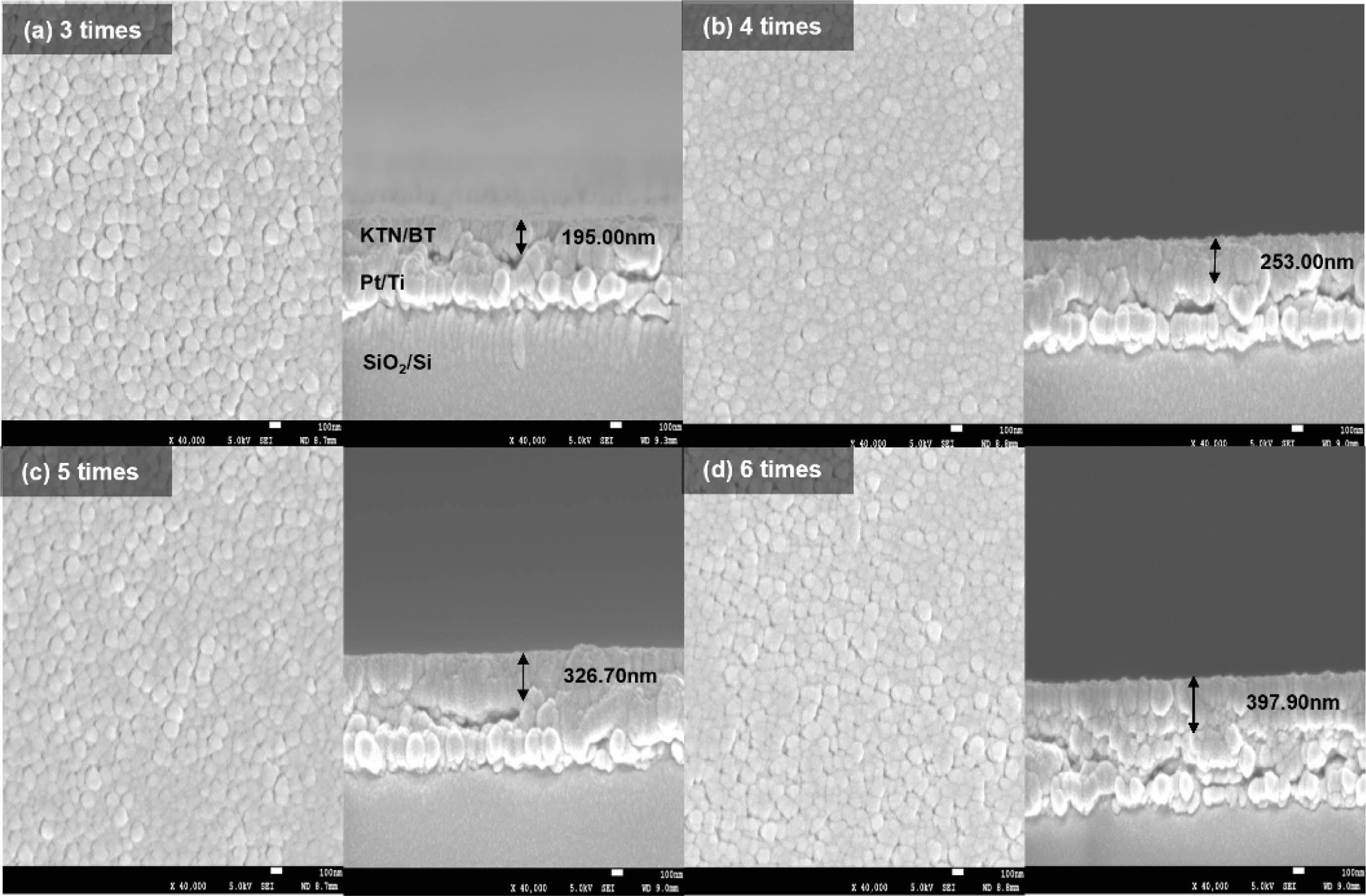
Fig. 3 shows a cross-sectional TEM photograph of the 6-times coated KTN/BT multilayer thin film. The interfaces between the KTN layers and BT layers are distinct, which is believed to be due to the difference in the crystal structure and the composition atoms between the K(Ta,Nb)O3 layer of the cubic structure and the BaTiO3 layer of the tetragonal structure. Additionally, the KTN layer (dark images) was observed to be thicker than the BT layer (bright images), which is considered to be due to the concentration difference between the KTN and BT precursor solutions. However, TEM images showed that the thickness of BT film varied irregularly with the number of coatings. Despite using the same coating conditions, the thickness variations were observed, and further experiments will be conducted to improve the films uniformity. In general, multilayer films show a proportional relationship between the structural and electrical properties and the number of coatings. Therefore, in this study, we coated the film up to 6 times.
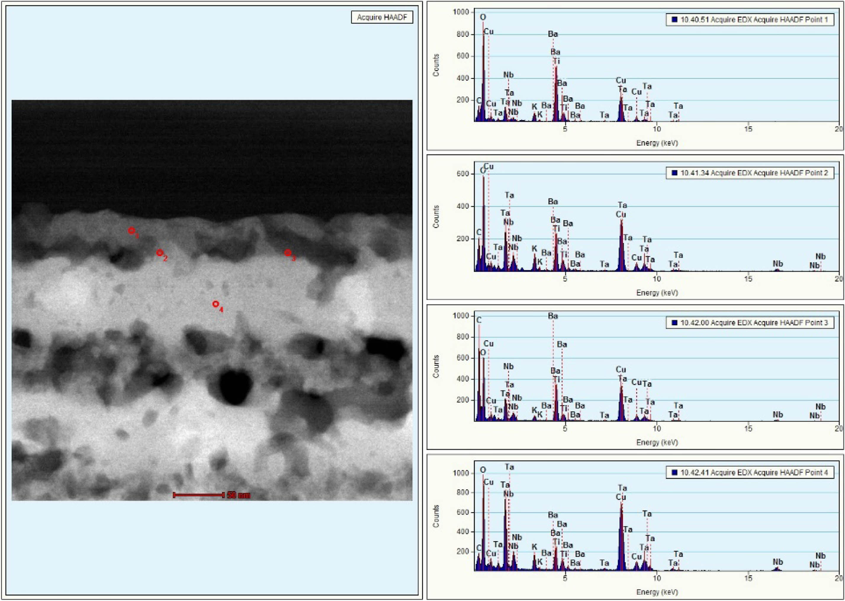
Fig. 4 shows the dark-field image of the cross-sectional TEM and the EDS analysis for observing the distribution of elements in the KTN/BT multilayer thin film. The interface between the KTN layer and BT layer showed non-uniform distributions. In the BT layer (point 1), high intensity peaks of Ba and Ti elements and low intensity peaks of K, Ta, and Nb elements were observed. In the KTN layer (point 4), high intensity peaks of K, Ta, and Nb elements and low intensity peaks of Ba and Ti elements were observed. However, at the KTN/BT interface (point 2, 3), the KTN and BT phases were observed to have almost the same peak intensities. It is considered that the coexistence of KTN phase and BT phase or the modified-KTN or -BT phases were caused by the diffusion of K, Ta, Nb, Ba, and Ti atoms to adjacent layers during the sintering process. Cu peaks were observed due to the substrate. As the thickness of KTN/BT films increased, the number of interfaces between KTN films and BT films increased, and it is thought to be due to an increase in ion displacement and a decrease in stress in the unit lattice by diffusion of K, Ta, Nb, Ba, and Ti at the interfaces [13]. Further investigations and discussions are needed to correctly understand the interfacial structure of KTN/BT multilayer thin films.
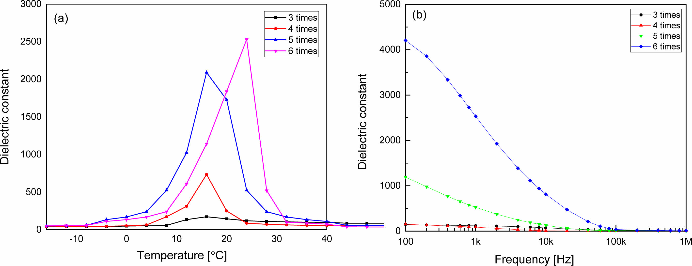
Fig. 5 shows dielectric constants according to the (a) temperature and (b) frequency of the KTN/BT multilayer thin films. The dielectric constant and Curie temperature increased as the number of coatings increased. This result is considered to be because as the number of coatings increases, the thickness of the film increases and the stress induced from the substrate decreases [13]. Curie temperature of KTN(65/35) crystal is about 0 °C [14], and BT has a transition temperature between tetragonal structure and orthorhombic structure near 0 °C. In this study, we measured dielectric properties in the range of –15 oC to 40 oC to observe the EC effect that can operate near room temperature. The transition temperature of the KTN/BT multilayer film coated 6 times was observed about 26 °C, and the maximum dielectric constant was 2530. It showed a typical dielectric relaxation characteristic where the dielectric constant gradually decreases as the frequency increases, which is believed to be due to the heterogeneous composition caused by the diffusion of atoms to adjacent layers. It is possible to obtain a good EC effect in a wide temperature range using the diffused phase transition properties, and in particular, in the case of a Curie temperature near room temperature, it can be applied to practical devices.
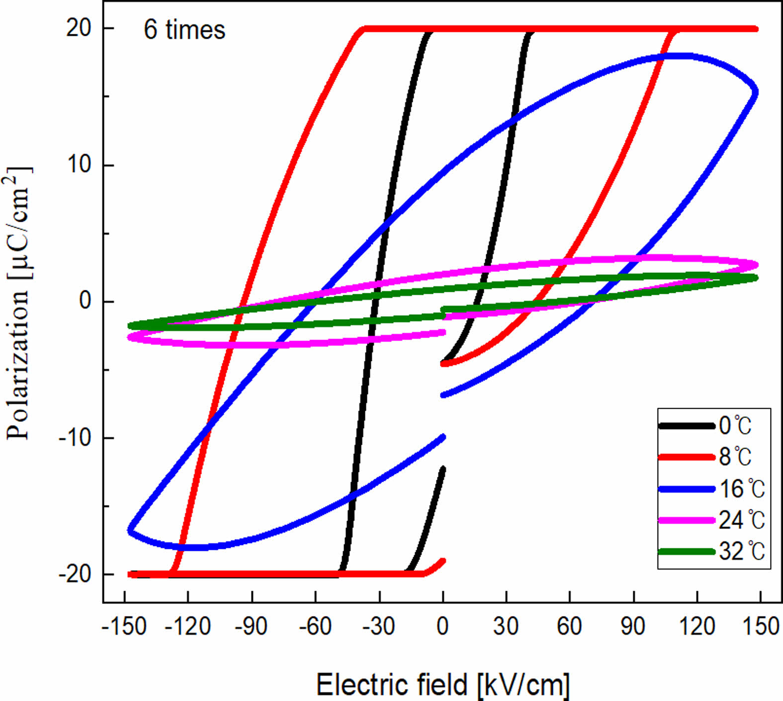
Fig. 6 shows the temperature-dependent P-E hysteresis loops of the 6-coated KTN/BT multilayer film. As the temperature increased, the saturation and squareness of the ferroelectric hysteresis loop decreased due to the decrease of the space charge polarization by thermal scattering, and the hysteresis loop gradually became thinner due to the decrease of the remnant polarization and coercive field.
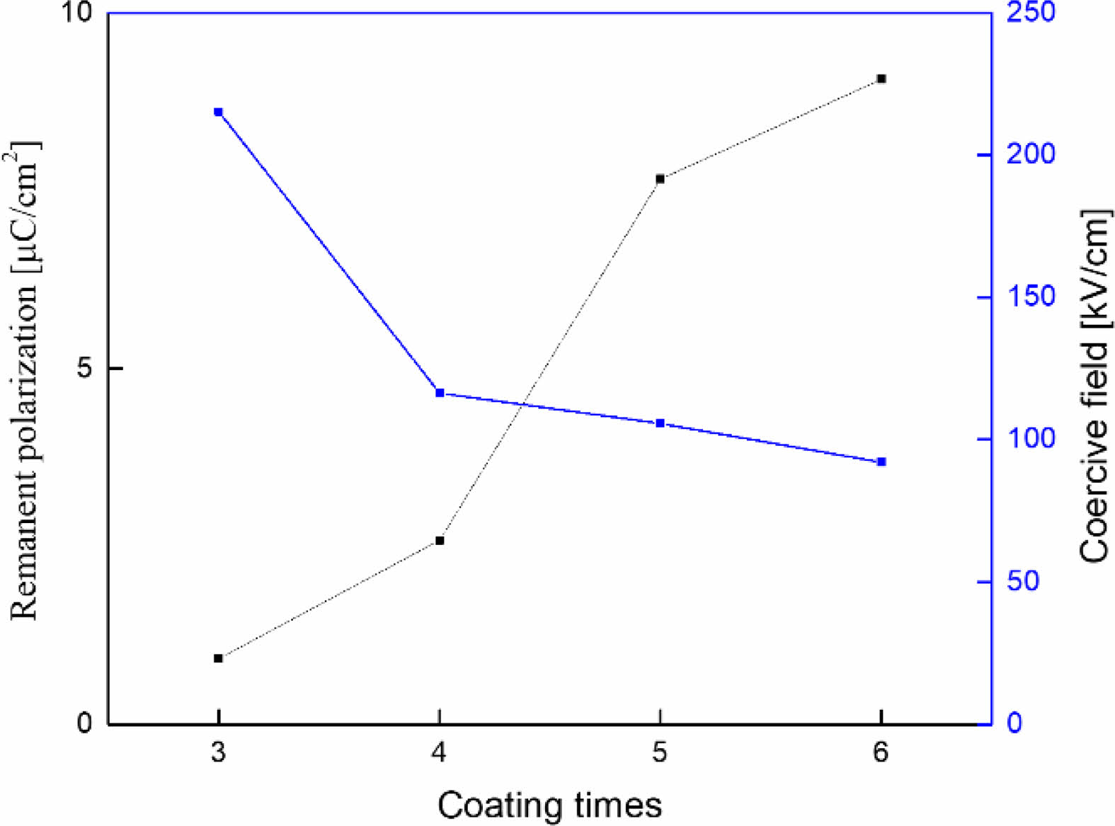
Fig. 7 shows the remnant polarization and the coercive field of the KTN/BT multilayer thin films measured at 16 °C. The remanent polarization increased and the coercive field decreased as the number of coatings and the film thickness increased. As shown in Fig. 5, it is believed that the influence of the stress induced from the interface between the KTN layer and Pt substrate decreases as the film thickness increases [13]. The remnant polarization and a coercive field of the 6-layer KTN/BT multilayer thin film exhibited superior properties of 9.2 μC/cm2 and 91 kV/cm, respectively, compared to the BT thin film [15].
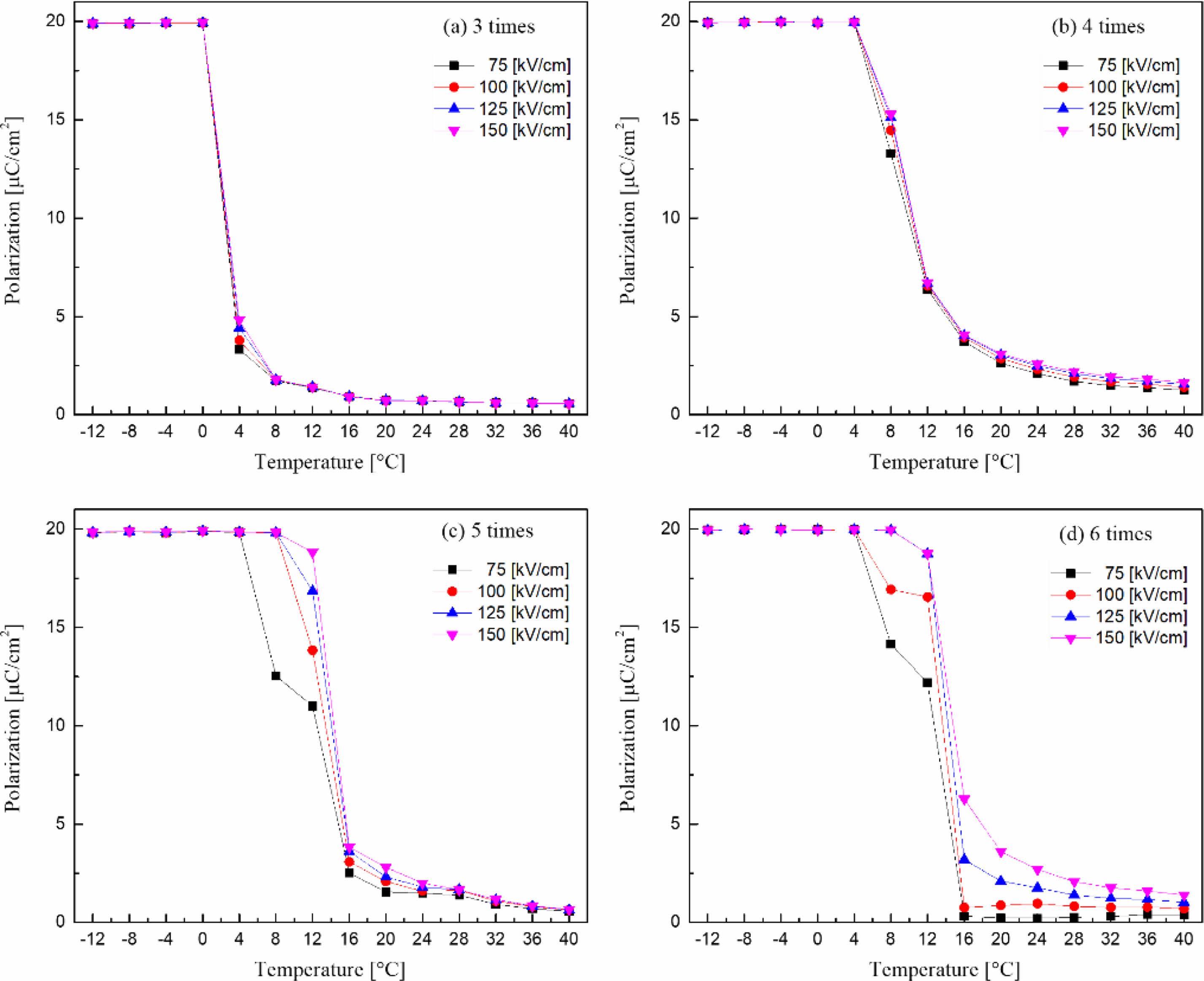
Fig. 8 shows the polarization according to the temperature and the applied electric field of the KTN/BT multilayer thin films. The temperature at which the polarization disappeared increased as the number of coatings increased, and ferroelectricity was shown at a temperature higher than the Curie temperature. In the 5- and 6-layer KTN/BT multilayer thin films, as the applied electric field increased, the temperature at which the ferroelectricity disappeared increased due to induced polarization by the electric field [16].
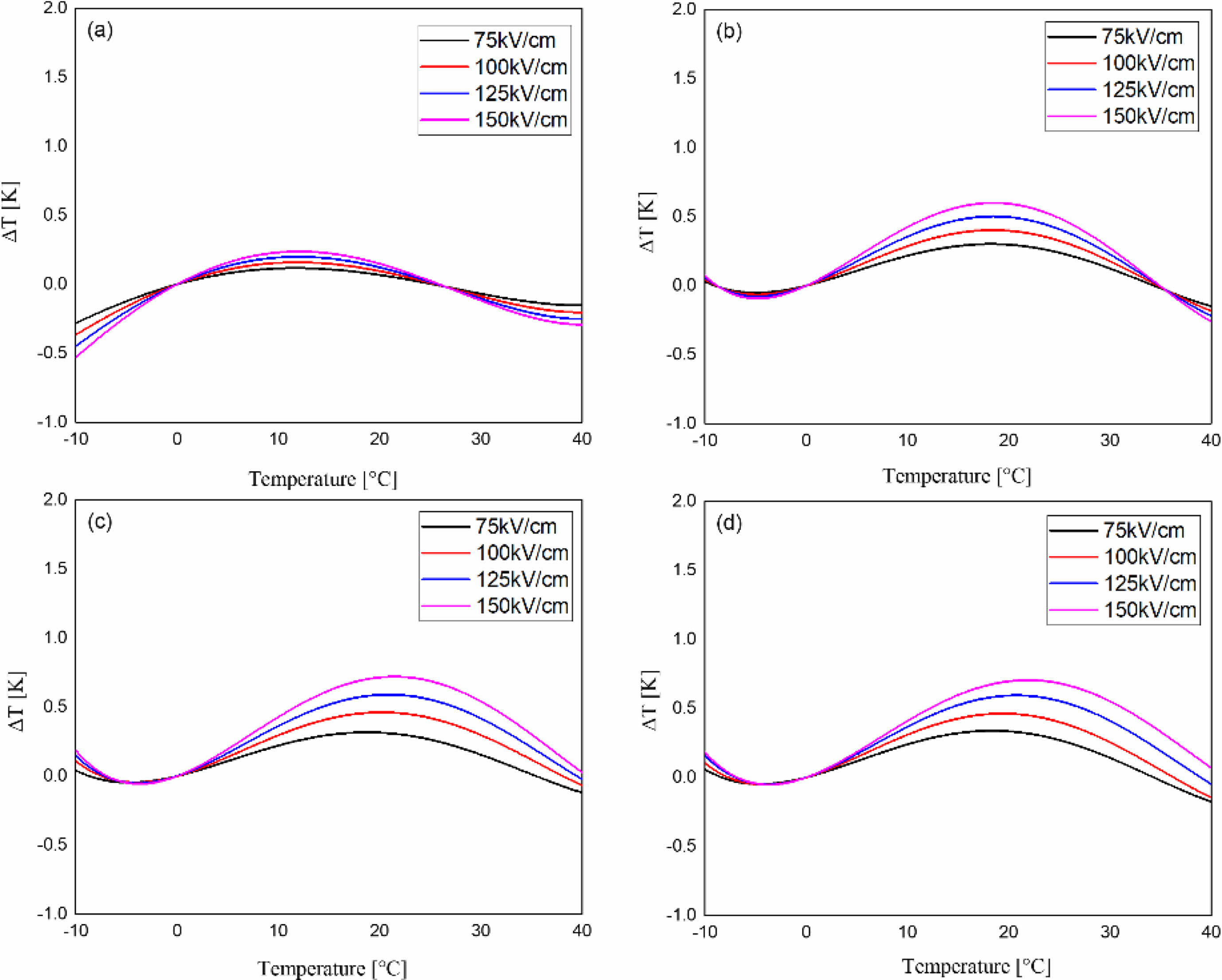
Fig. 9 shows the electrocaloric temperature change (ΔT) according to the applied electric field of the KTN/BT multilayer thin films. ΔT was calculated from the following equation [17]:
Here, C and ρ are the specific heat and the density, respectively. The specific heat and density of BT [18] are 434 J/Kg·K and 6.08 g/cm3, respectively, and those of KTN [19] are 303.15 J/Kg·K and 6.231 g/cm3, respectively. In this study, we used these data considering the volume ratio of KTN/BT multilayer films. The maximum ΔT occurred at a temperature higher than the Curie temperature, which is believed to be due to the coexistence of ferroelectric and paraelectric phases caused by diffused phase transition and the easy switching characteristics of dipole moments in the applied electric field [20]. ΔT increased as the applied electric field increased, which is believed to be due to induced polarization by the electric field. The 5-layer KTN/BT multilayer thin film with an electric field of 150 kV/cm exhibited the highest ΔT of 0.72 K at 22 °C.
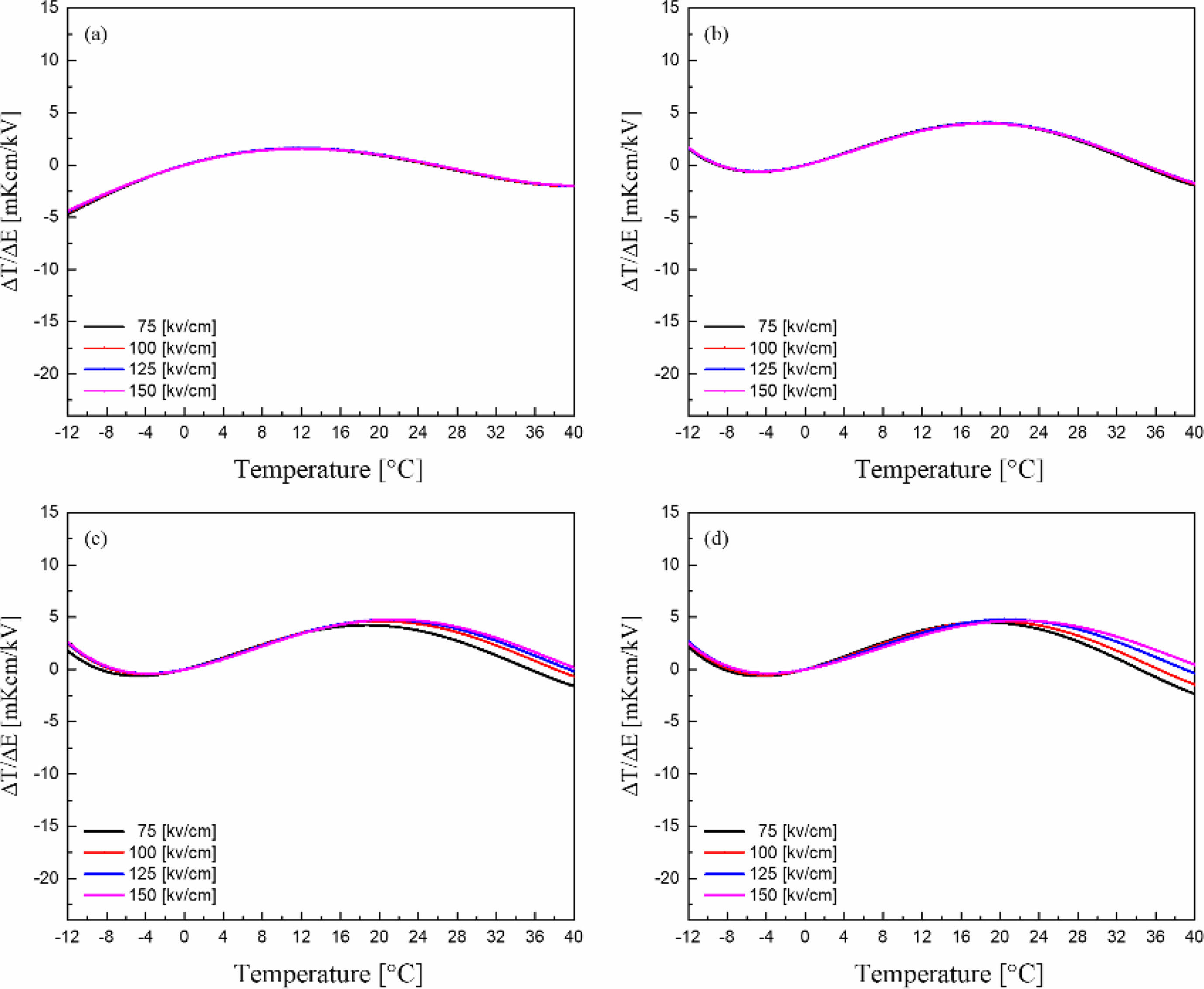
Fig. 10 shows the EC strength (ΔT/ΔE) [21] of the KTN/BT multilayer thin films. The 5-layer KTN/BT multilayer thin film with an electric field of 150 kV/cm showed a maximum value of 4.8 mK·cm/kV at 20 °C. All specimens showed good ΔT/ΔE properties in a wide temperature range near room temperature, which is considered to be due to the diffused phase transition properties caused by the repeated multilayer structure of KTN film and BT film [22]. Therefore, it would be possible to fabricate cooling devices with a Curie temperature near room temperature and a good electric calorific effect in a wide temperature range using multilayer thin films made of materials with different structural and electrical properties. In the future, we will continue to study the EC effects through crystalline characteristics control such as superlattice structure or morphotropic phase boundary (MPB) at the interface of the multilayer thin films.
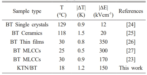
Table 1 shows the electrocaloric properties of BT single crystal, ceramics, thin films and MLCCs [23]. Single crystals and ceramics exhibit high electrocaloric properties due to their first-order phase transition characteristics, while exhibiting low dielectric breakdown voltage characteristics. However, thin films and MLCC specimens exhibit relatively good electrocaloric properties and high dielectric breakdown voltage. KTN/BT multilayer film fabricated in this study exhibited good EC properties near room temperature, and it is considered to be applicable as a cooling device at room temperature.
|
Fig. 1 XRD patterns of KTN/BT multilayer thin films. |
|
Fig. 2 Surface and Cross-sectional microstructures of KTN/BT multilayer thin films. |
|
Fig. 3 Cross-sectional TEM photograph of 6-times coated KTN/ BT multilayer thin film. |
|
Fig. 4 The dark-field image of the cross-sectional TEM and the EDS analysis for observing the elements distribution of the KTN/ BT multilayer thin film. |
|
Fig. 5 Dielectric constant according to the (a) temperature and (b) frequency of KTN/BT multilayer thin films. |
|
Fig. 6 P-E hysteresis loop of the 6-coated KTN/BT multilayer thin film. |
|
Fig. 7 Remnant polarization and coercive field of KTN/BT multilayer thin films measured at 16 oC. |
|
Fig. 8 The polarization according to the temperature and applied electric field of KTN/BT multilayer thin films. |
|
Fig. 9 The electrocaloric temperature change (ΔT) according to the applied electric field of the KTN/BT multilayer thin films. |
|
Fig. 10 EC strength (ΔT/ΔE) of the KTN/BT multilayer thin films. |
In this paper, KTN/BT multilayer thin films were prepared by using the sol-gel method and spin coating method, and the applicability to the EC material was investigated. The average grain size was about 92 to 95 μm, showing a uniform and dense microstructure. The heterogeneous interfacial layers at the KTN/BT multilayer thin film interfaces were caused by the diffusion of K, Ta, Nb, Ba, Ti elements to adjacent KTN or BT layers during the sintering process. It showed typical dielectric relaxation characteristics in which the dielectric constant decreases as the frequency increases. As the thin film thickness increased, the remanent polarization increased and the coercive field decreased. ΔT increased as the applied electric field increased and the maximum ΔT occurred at a temperature higher than the Curie temperature. It is believed that phase transition temperature control and an excellent EC effect could be obtained from multilayer thin films using materials with different structural and electrical properties.
This research was supported by Basic Science Research Program through the National Research Foundation of Korea (NRF) funded by the Ministry of Education (2020R1A6A1A03038697) and This work was supported by the National Research Foundation of Korea (NRF) grant funded by the Korea government (MSIT) (2021R1I1A3052426). And this work was partly supported by Korea Evaluation Institute of Industrial Technology (KEIT) grant funded by the Korea government (MOTIE) (No. 20020478, Development of commercial reference materials for chemical composition of nano-grade aluminum oxide for rechargeable battery separator coating).
- 1. B.S. Bibin and E. Gundabattini, International Journal of Air-Conditioning and Refrigeration 29[3] (2021) 2130005.
-

- 2. E. Birks, M. Dunce, and A. Sternberg, Ferroelectrics 400[1] (2010) 336-343.
-
- 3. S. Patel, H. Yadav, and M. Kumar, J. Korean Ceram. Soc. 58[4] (2021) 437-444.
-
- 4. L. Shaobo and L. Yanqiu, Mater. Sci. and Eng. B 113[1] (2004) 46-49.
-
- 5. J.H. Qiu and Q. Jiang, J. Appl. Phys. 103[8] (2008) 084105.
-
- 6. S. Lu and Q. Zhang, J. Adv. Dielectrics 2[3] (2012) 1230011.
-
- 7. A.S. Mischenko, Q. Zhang, J.F. Scott, R.W. Whatmore, and N.D. Mathur, Science 311[5765] (2006) 1270-1271.
-
- 8. K. Nakamura, J. Miyazu, M. Sasaura, and K. Fujiura, Appl. Phys. Lett. 89 (2006) 131115-1-3.
-
- 9. M. Kwon, J. Kim, J. Park, and S. Lee, J. Ceram. Proc. Res. 21[6] (2020) 725-730.
-
- 10. M. Kwon, S. Lee, and K. Kim, J. Nanosci. Nanotechnol. 18[9] (2018) 5936-5941.
-
- 11. R. Ashiri, A. Nemati, and M. Ghamsari, Ceramics International 40[6] (2014) 8613-8619.
-
- 12. D.D. Liu, J.J. Ho, R.C. Pastor, and O.M. Stafsudd, Mat. Res. Bull. 27[6] (1992) 723-729.
-
- 13. S.G. Lee and Y.H. Lee, Thin Solid Films 353 (1999) 244-248.
-
- 14. S. Lee, I. Park, S. Bae, and Y. Lee, Jap. J. Appl. Phys. 36[11A] (1997) 6880-6883.
-
- 15. T. Hyayshi, N. Oji, and H. Maiwa, Jpn. J. Appl. Phys. 33[9] (1994) 5277-5280.
-
- 16. S. Triebwasser, Physical Review 114[1] (1959) 63-70.
-
- 17. J. Fernanedz, B. Bindhu, M. Prabu, and K. Sandhya, J. Korean Ceram. Soc. 59[2] (2022) 240-251.
-
- 18. L. Bellaiche, A. Garcia, and D. Vanderbilt, Phys. Rev. B 64 (2001) 060103.
-
- 19. B.A. Tuttle, Thesis, University of Illinois at Urbana-Champaign, ProQuest Dissertation Pub. 1981, 8203624.
- 20. Y. He, Thermochemica Acta 419[1-2] (2004) 135-141.
-
- 21. O.M. Stafsudd and M.Y. Pines, J. Opt. Soc. Am. 62[10] (1972) 1153-1155.
-
- 22. B. Park, S. Lee, M. Lee, J. Park, B. Kim, and S. Lee, J. Ceram. Proc. Res. 23[3] (2022) 252-256.
-
- 23. X. Moya, E. Stern-Taulats, S. Grossley, D. Gonzalez-Alonso, S. Kar-Narayan, A. Planers. L. Manosa, and N. D. Mathur, Adv. Mater. 25[9] (2013) 1360-1365.
-
- 24. J. Zhang, Y. Zhang, Q. Chen, X. Chen, G. Wang, X. Dong, J. Yang, W. Bai, and X. Tang, Nanomaterials 11[8] (2021) 2141.
-
- 25. J. Li, A. Torello, Y. Nouchokgwe, T. Granzow, V. Kovacova, S. Hirose, and E. Defay, J. of Physics: Energy 5[2] (2023) 024017.
-
- 26. X. Moya, E. Stern-Taulats, S. Crossley, D. González-Alonso, S. Kar-Narayan, A. Planes, L. Manosa, and N. D. Mathur, Adv. Mater. 25[9] (2013) 1360-1365.
-
- 27. Y. Bai, S. Qin, W. Nie, J. Li, J. Li, H. Wang, L. Qiao, and D. Guo, Ceram. Int. 44 (2018) 8263-8269.
-
- 28. B. Magalhaes, S. Engelhardt, C. Molin, S.E. Gebhardt, K. Nielsch, and R. Hühne, J. Alloys Compd. 891 (2022) 162041.
-
- 29. S. Kar-Narayan and N.D. Mathur, J. Phys. D: Appl. Phys. 43[3] (2010) 032002.
-
 This Article
-
2024; 25(1): 48-55
Published on Feb 29, 2024
- 10.36410/jcpr.2024.25.1.48
- Received on Oct 5, 2023
- Revised on Nov 27, 2023
- Accepted on Nov 29, 2023
Services
- Abstract
introduction
experimental
results and discussion
conclusion
- Acknowledgements
- References
- Full Text PDF
Shared
Correspondence to
- Sung-Gap Lee
-
Dept. of Materials Engineering and Convergence Technology, RIGET, Gyeongsang National University, Jinju 52828, Korea
Tel : +82-10-2686-4427 Fax: +82-55-772-1689 - E-mail: lsgap@gnu.ac.kr
Clean-Energy Research Institute(CRI), Hanyang University, 222, Wangsimni-ro, Seongdong-gu, Seoul, 04763, Korea
E-mail: jcpr@hanyang.ac.kr