


- Effects of deposition of an ultra-thin Al2O3 layer via atomic layer deposition on electrochromic property, self-discharge, and discharge capacity of photo-electrochromic devices
Woon-Yong Parka, Yoon-Tae Parka, Byung Guk Ahna,b,* and Ki-Tae Leea,b,c,d,*
aDivision of Advanced Materials Engineering, Jeonbuk National University, Jeonbuk 54896, Republic of Korea
bHydrogen and Fuel Cell Research Center, Jeonbuk National University, Jeonbuk 54896, Republic of Korea
cDepartment of Energy Storage/Conversion Engineering of Graduate School (BK21 FOUR), Jeonbuk National University, Jeonbuk 54896, Republic of Korea
dDepartment of JBNU-KIST Industry-Academia Convergence Research, Jeonbuk National University, Jeonbuk 54896, Republic of KoreaThis article is an open access article distributed under the terms of the Creative Commons Attribution Non-Commercial License (http://creativecommons.org/licenses/by-nc/4.0) which permits unrestricted non-commercial use, distribution, and reproduction in any medium, provided the original work is properly cited.
Photo-electrochromic devices (PECDs) can be spontaneously colored by sunlight and used as energy storage devices. The major obstacle to improving the performance of PECDs is the self-discharge at the interface between electrolyte and electrochromic layers. To prevent self-discharge, we deposited ultra-thin Al2O3 films on the WO3 electrochromic layer using atomic layer deposition (ALD). The ALD-deposited Al2O3 layer effectively suppressed the self-discharge phenomenon that results from the reduction of iodine. Therefore, the transmittance modulation (ΔT), photocharged voltage, and discharge capacity increased with an increasing number of ALD cycles. Specifically, the discharge capacity of the PECD-A5 sample fabricated with five ALD cycles increased by 63.7% compared to the PECD without an Al2O3 layer. However, the relatively thick Al2O3 layer of the PECD-A10 sample fabricated with ten ALD cycles resulted in performance degradation due to the slow Li+ ion diffusion rate.
Keywords: Photo-electrochromic device, Electrochromic property, Self-discharge, Discharge capacity, Atomic layer deposition.
Electrochromic devices (ECDs) that modulate light transmittance through electrochemical oxidation-reduction reactions are widely used in energy-efficient buildings, reflective displays, and smart windows [1]. Recently, the function of ECDs has expanded into photo-electrochromic devices (PECDs), which combine an electrochromic electrode and a dye-sensitized solar cell (DSSC) electrode [2]. Unlike conventional ECDs that require an external power source to achieve a color change, PECDs can spontaneously darken when illuminated by sunlight [3]. In this regard, many studies seek to leverage PECD optical properties, such as color intensity reflecting the real-time energy level stored within PECDs [4-6].
Tungsten oxide (WO3) is a conventional material for PECDs as well as ECDs due to its high coloration efficiency and excellent electrochemical stability. However, WO3 thin films produced by conventional thermal evaporation or sputtering methods are too dense, which limits Li+ ion diffusion and slows conversion speed [7, 8]. Although various nanostructures have been proposed to overcome this slow reaction process, there are difficulties in achieving a practical ultrafast response rate. Small interconnected porous structures are ideally suited to achieve the desired reaction time [9-12]. Meanwhile, amorphous WO3 films prepared by electrodeposition or spin coating exhibit fast Li+ ion diffusion rates and excellent coloring efficiencies [13-18].
Since Li+ ions are intercalated into WO3 in the colored state, the PECD can be used as an energy storage device. In other words, when an external load is applied in the dark field, Li+ ions de-intercalate, and discharge becomes possible. However, the biggest hinderance to such an application of PECDs is self-discharge in the WO3 layer. Self-discharge is a phenomenon that takes place in an electrochemical cell such as a battery, in which the stored charge diminishes over time due to an internal chemical reaction, even in the absence of an external circuit connection [19-21]. This phenomenon occurs at the interface between the electrode and the electrolyte [22, 23].
Al2O3 is widely known as a non-conductive material that imposes severe restrictions on the flow of electrons and ions. As a result, it can be used to alleviate the self-discharge of PECDs, though it must be deposited in extremely thin layers. Therefore, utilization of atomic layer deposition (ALD) is the optimal method to achieve the desired deposition thickness while avoiding the side effects of electronic and ionic mobility constraints [24-27].
In this study, we aimed to improve the discharge capacity of PECDs with amorphous WO3 films by suppressing the self-discharge phenomenon through the deposition of ultra-thin Al2O3 layers via ALD. The correlation between self-discharge and the Al2O3 protection layer deposited by ALD was investigated.
Fabrication of a WO3 electrochromic layer
In the first step of the fabrication procedure, a WO3 precursor solution was prepared by dissolving tungsten metal powder (99.9%, Sigma Aldrich, USA) in hydrogen peroxide (30-35.5%, Samchun Chemical, Korea) and deionized (DI) water, as described in our previous study [28]. Upon completion of the reaction, a colorless solution known as peroxotungstic acid (PTA) was produced. After filtration to remove supersaturated tungsten metal powder, the PTA solution was added to 2-propanol (99+%, Thermo Fisher Scientific, USA) in a volume ratio of 4:9. The prepared coating solution was aged at room temperature for 48 h. To prepare for subsequent steps, indium-doped tin oxide (ITO)-coated glass (ITO/glass, STN 10, UID, Korea) with a sheet resistance of 6-9 Ω/square was cleaned in acetone (Daejung Chemicals % metals Co., 99.5%), 2-propanol (Alfa Aesar, 99+%), and then DI-water for 10 min each and dried using an air gun. To fabricate WO3 films on ITO/glass, electrodeposition was carried out using a DC power supply. In this process, a current of 10 mA and a voltage of 10 V were applied for 60 s, with Pt wire utilized as a counter electrode. The deposited WO3 films were washed with DI water and ethanol and then thoroughly dried at 100 ℃ in a vacuum oven. The average thickness of the as-deposited films WO3 was approximately 200 nm.
ALD of Al2O3 onto a WO3 electrochromic layer
ALD of Al2O3 onto electro-deposited WO3 was carried out using a tube-type thermal ALD system (IH-10, I TECH U Co., Korea). Deposition was performed using successive pulses of trimethylaluminum (TMA) precursor and DI-water reactant at 150 ℃. TMA and H2O were dosed for 1 s each and Ar was purged for 10 s after each pulsing step. The growth rate of the Al2O3 thin films on p-type Si was measured to be 1.1 Å/cycle, which is consistent with results from previous studies [24-26]. Films were fabricated with either 1, 5, or 10 ALD cycles. For comparison, a WO3 thin film was also prepared without Al2O3 deposition under identical electrodeposition conditions.
Fabrication of photoelectrodes
Fluorine-doped tin oxide (FTO)-coated glass (TEC 8, Pilkington, UK) with a sheet resistance of 6-9 Ω/square was cleaned using the same process as for ITO/glass. Screen printing of TiO2 paste (Ti-Nanoixde T/SP, Solaronix, Switzerland) was used for mesoporous TiO2 film deposition, and the films were sintered at 500 ℃ for 30 min in a muffle furnace at a heating rate of 10 ℃/min. The final thickness of the TiO2 film was approximately 9 μm. After finishing the sintering step, the TiO2 films were dipped in a prepared 0.3 mM (bis(tetrabutylammonium)-cis-di(thiocyanato)-N,N’-bis(4-carboxylato-4’-carboxylic acid-2,2-bipyridine) ruthenium (Ⅱ) (N719, Solaronix, Switzerland) solution in ethanol under dark conditions at room temperature for 24 h [29].
Assemble of PECDs
For assembly of the PECDs, the prepared photoelectrode and electrochromic counter electrode were sealed using a 60-μm-thick Surlyn film (Solaronix, Switzerland). Electrolyte (AN-50, Solaronix, Switzerland) containing 50 mM of iodine redox ions (I2/LiI) was injected through the holes, which then were sealed with cover glass and Surlyn films. The active areas of the photoelectrode and electrolyte were 0.25 cm2 and 1.0 cm2, respectively. The final fabricated PECDs were denoted as PECD-A0, PECD-A1, PECD-A5, and PECD-A10, with the final number indicating the number of ALD cycles used in the fabrication.
Characterization
X-ray diffraction (XRD) was carried out using an X-ray diffractometer (MAX-2500, Rigaku, Japan) with Cu Kα radiation to analyze crystal structure and phases. Diffraction patterns were recorded at a scan rate of 4o/min over a 2θ range of 20 to 60o. The existence of Al2O3 in the samples was analyzed by X-ray photoelectron spectroscopy (XPS, Nexsa-XPS system, Thermo Scientific, USA) with monochromatic Al Kα radiation as the X-ray source. The optical properties were evaluated by UV-visible spectroscopy (Agilent 8453, Agilent Technologies, USA). The surface morphologies of the as-deposited thin films were analyzed by a high-resolution-scanning electron microscope (HR-SEM, SU8230, Hitachi, Japan).
Photocurrent density-voltage (J-V) characteristics of the PECDs were evaluated under standard illumination conditions (100 mW/cm2, AM 1.5G) using a source meter (Keithely 2400, Tekronix) in the range of ±1 V and scan step of 0.02 V with a delay time of 0.5 s. In-situ transmittance data were collected using a He-Ne laser with a wavelength of 632.8 nm. The open circuit voltage decay (OCVD) method was performed using a potentiostat (SP150, Biologic SAS, France) in a frequency range of 9 mHz to 100 kHz to verify the electrochemical reaction in the PECDs.
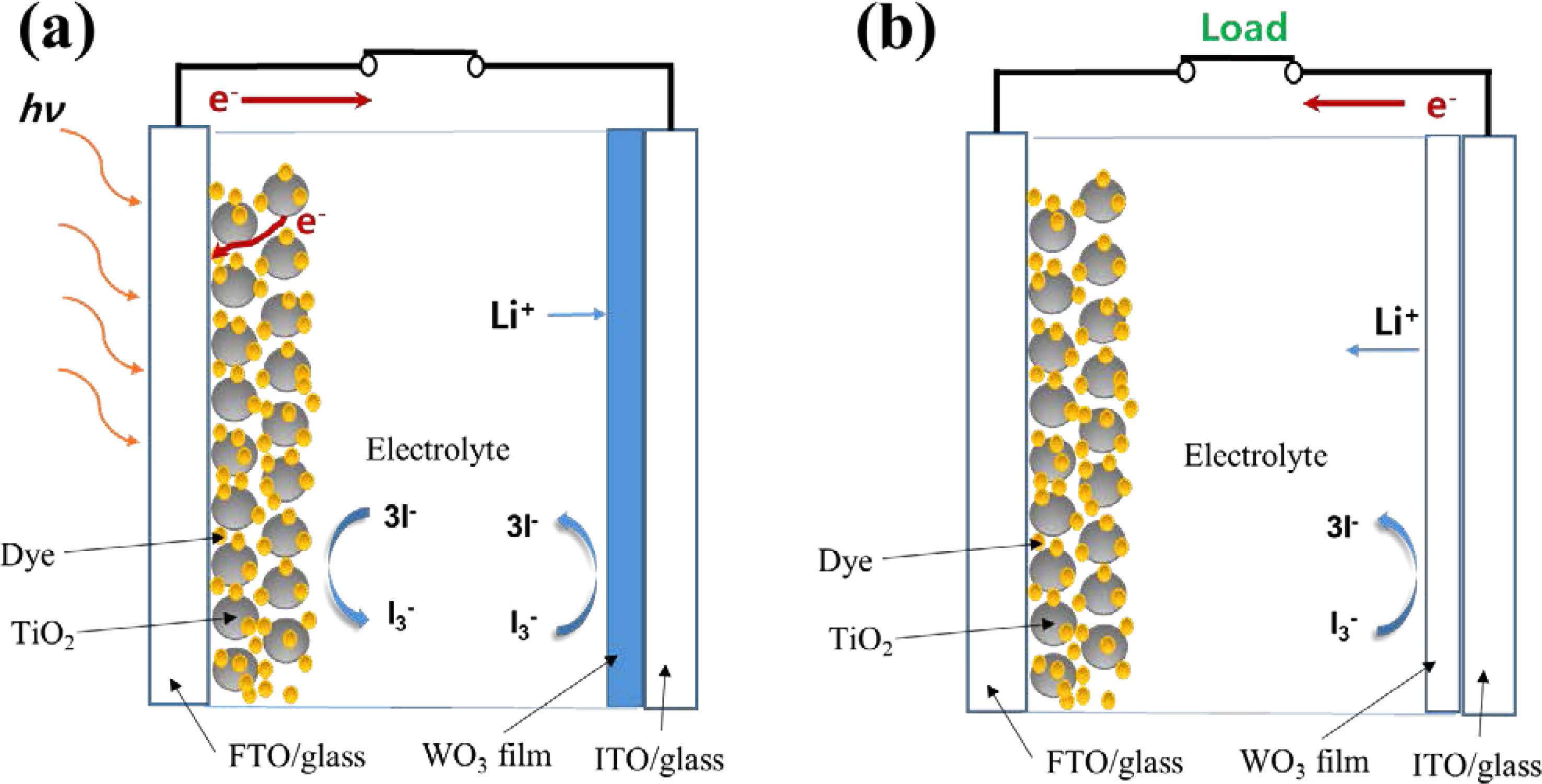
The operation mechanism of the PECD is described schematically in Fig. 1. Upon illumination in a short circuit condition (Fig. 1a), photoelectrons are generated in the photosensitive N719 dye molecules, and electrons are injected from the conduction band of the dye to the conduction band of the TiO2 and then to FTO. The photoelectrons generated from the photoelectrode reach the WO3 thin film via an external circuit accompanying the intercalation of Li+ ions, leading to the photocharging associated with blue coloration in the PECD. When WO3 thin film is colored and the light is blocked, a voltage equal to the circuit photovoltage appears with opposite polarity across the PECD. When a load is applied (Fig. 1b), the built-up voltage drives the bleaching process of the PECD by removing electrons and Li+ ions from the colored LixWO3 film in the battery-like discharge process. However, when the light is blocked, the bleaching process may occur even in an open circuit without an external control due to self-discharge.
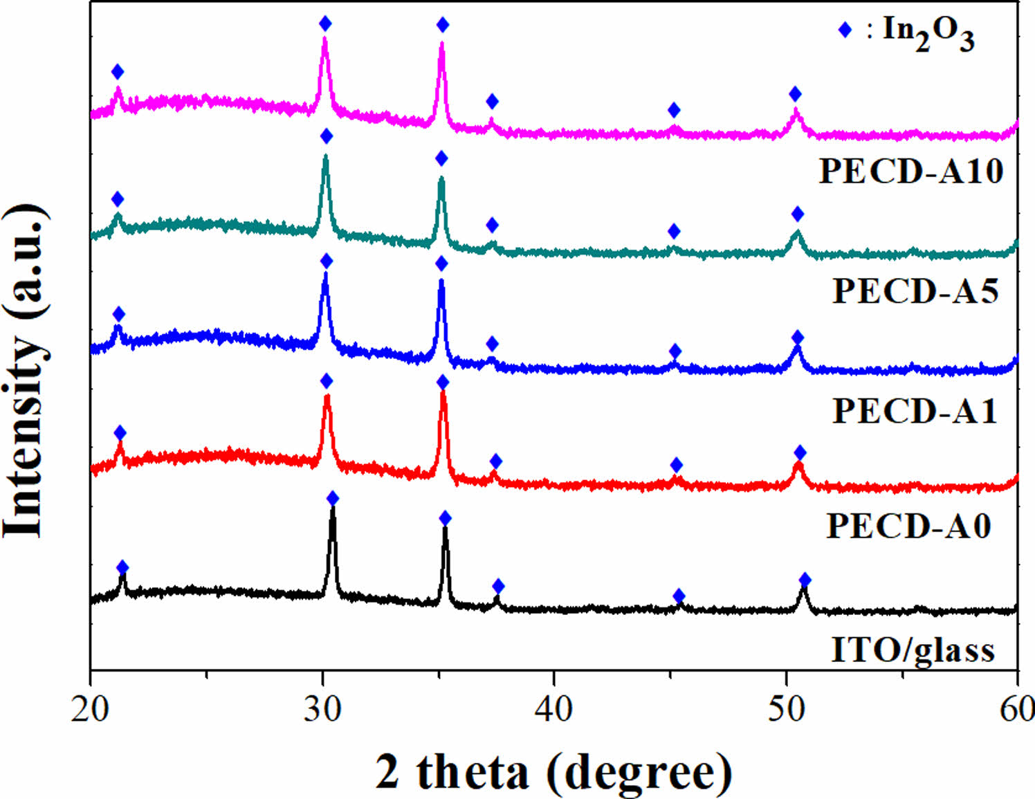
X-ray diffraction patterns of the WO3 thin films with and without an Al2O3 deposition layer are shown in Fig. 2, along with the diffraction from an ITO substrate as a reference. No distinct peaks except for those from the ITO substrate and broad reflections between 20 and 30 degrees were observed, indicating that the WO3 thin films fabricated by electrodeposition were amorphous. Moreover, no significant change in the crystal structure occurred due to the presence of the ALD-deposited Al2O3, peaks of which were not detected due to the small amount deposited.
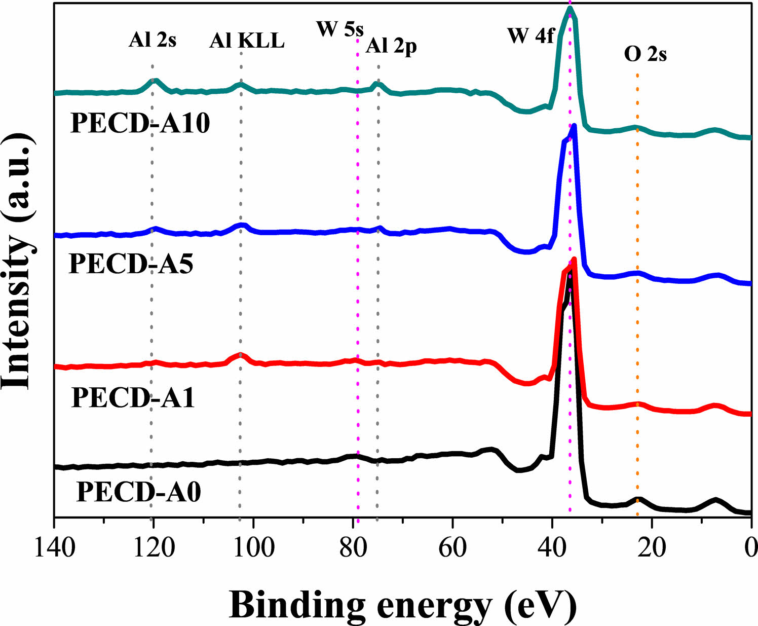
XPS analysis was carried out to confirm the existence of Al2O3. The survey spectra of the WO3 thin films with and without an Al2O3 deposition layer are shown in Fig. 3. All samples with Al2O3 deposition layers exhibited Al 2s, Al 2p, and Al KLL peaks. The intensity of the Al peaks increased with increasing number of ALD cycles.
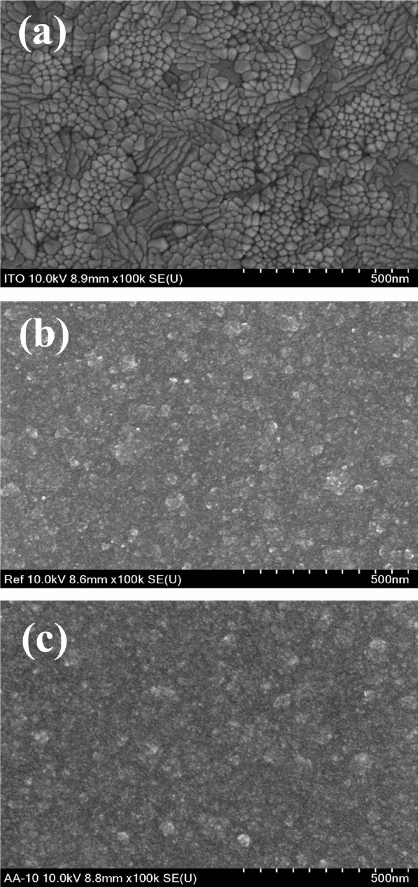
Figure 4 shows HR-SEM images of a bare ITO substrate and the WO3 thin films with and without an Al2O3 deposition layer. The surface of the WO3 thin film fabricated by electrodeposition (PECD-A0) was macroscopically uniform, grainy, and compact, with no surface porosity along the ITO surface, as shown in Fig. 4b. For the WO3 thin film with Al2O3 deposited through 10 ALD cycles (PECD-A10), no significant change in the surface morphology was observed, as shown in Fig. 4c. This consistency in observed surface morphology is due to the extremely thin Al2O3 layer of about 1 nm thickness.
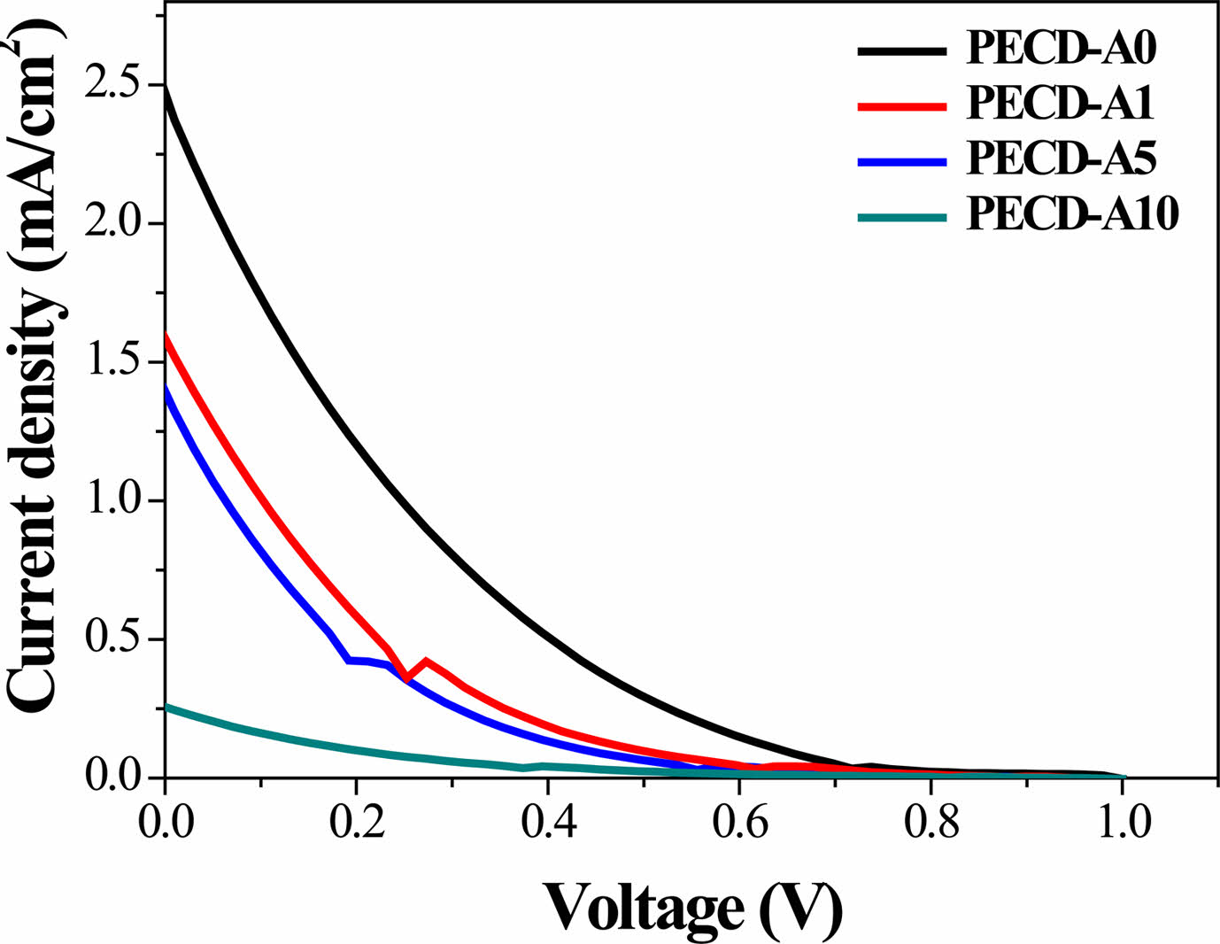
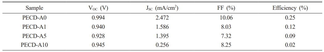
J-V characteristic measurements were conducted to evaluate the photovoltaic performance of the PECDs as a function of the number of Al2O3 ALD cycles (Fig. 5, photovoltaic parameters are also shown in Table 1). In a general DSSC system, Pt is used as the counter electrode for regeneration of I3−/3I− redox mediator (I3− + 2e− → 3I−). However, in the present PECD, the electrochromic WO3 layer was used as the counter electrode instead of Pt. Because WO3 has a very low catalytic activity compared to Pt, this PECD exhibited low J-V performance. Moreover, because insulating Al2O3 was deposited on the WO3, the efficiency further decreased with increasing number of ALD cycles, as shown in Fig. 5 and Table 1. Despite its relatively low performance as a DSSC, the WO3 electrochromic layer of the PECD was spontaneously colored via photocharging.
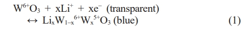
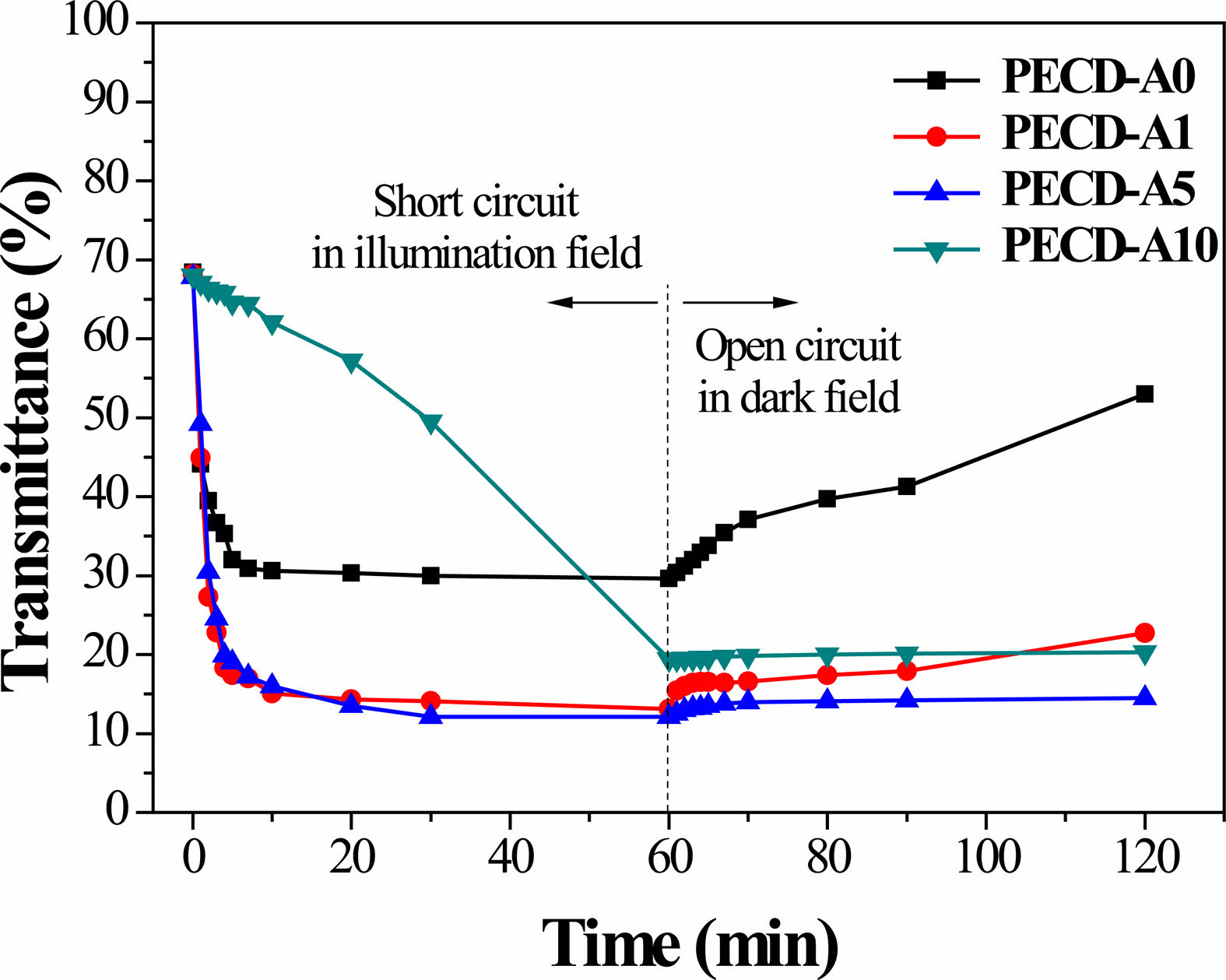
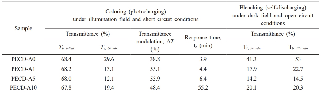
Figure 6 shows the in-situ optical transmittance spectra obtained from the PECDs according to number of Al2O3 ALD cycles. While the coloring process (photocharging process) was carried out in short circuit and under an illumination field, the bleaching process (self-discharging process) was carried out in open circuit and under dark field. Based on the optical transmittance data, the transmittance modulation (ΔT = Tb - Tc, where Tb and Tc are the transmittance values in the bleached and colored state, respectively) and response time tc (or tb) based on a transmittance modulation depth of 90% can be calculated [28]. The overall electrochromic performance parameters measured from the PECDs are listed in Table 2. Unlike conventional ECDs, the PECDs could be colored under an illumination field and bleached under dark field without any external voltage application. The electrochromic redox behavior of the WO3 films is based on the Li+ ion intercalation/de-intercalation reaction:
Electrons generated from the photoelectrode by illumination of the PECDs are transferred to WO3 via the external circuit, and Li+ ions are inserted from the electrolyte for charge compensation; the transparent WO3 films turn blue upon reduction. However, due to the reduction of iodine (I3− + 2e− → 3I−) at the interface between the electrolyte and WO3 layer in the PECDs, the ΔT value of the PECDs is lowered compared to those of conventional ECDs without iodine. As shown in Fig. 6 and Table 2, the ΔT value of the PECDs increased as the number of Al2O3 ALD cycles increased up to five cycles and then decreased with the PECD-A10 sample. The deposition of Al2O3 through ALD physically diminishes the interface area between the electrolyte and WO3. The increase in Al2O3 thickness may be preventing the reduction of iodine at the electrolyte-WO3 interface during illumination. Therefore, a relatively large number of Li+ ions can be inserted due to the relatively large number of accumulated electrons, and the ΔT value of the PECDs increases accordingly. However, with the PECD-A10 sample, which has a thick Al2O3 layer of about 1 nm, the reduction in diffusion rate of Li+ ions is much greater than the suppression of iodine reduction, resulting in a decrease in ΔT. Similarly, the response time for coloration (tc) increased with increasing number of Al2O3 ALD cycles because the diffusion rate of Li+ ions slowed as the thickness of the Al2O3 layer increased.
Under dark field conditions, LixW1-x6+Wx5+O3 released both electrons and Li+ ions, accompanied by the reduction of iodine in the electrolyte of the PECDs, even in an open circuit condition, resulting in bleaching or self-discharging. As shown in Fig. 6 and Table 2, with the PECD-A0 sample that does not contain a Al2O3 layer, the transmittance value increased rapidly over time with number of Al2O3 ALD cycles, whereas the transmittance value increased only slightly. In particular, the transmittance value was well maintained in the PECD-A10 sample, indicating that the Al2O3 layer deposited by ALD effectively suppresses the self-discharge phenomenon.
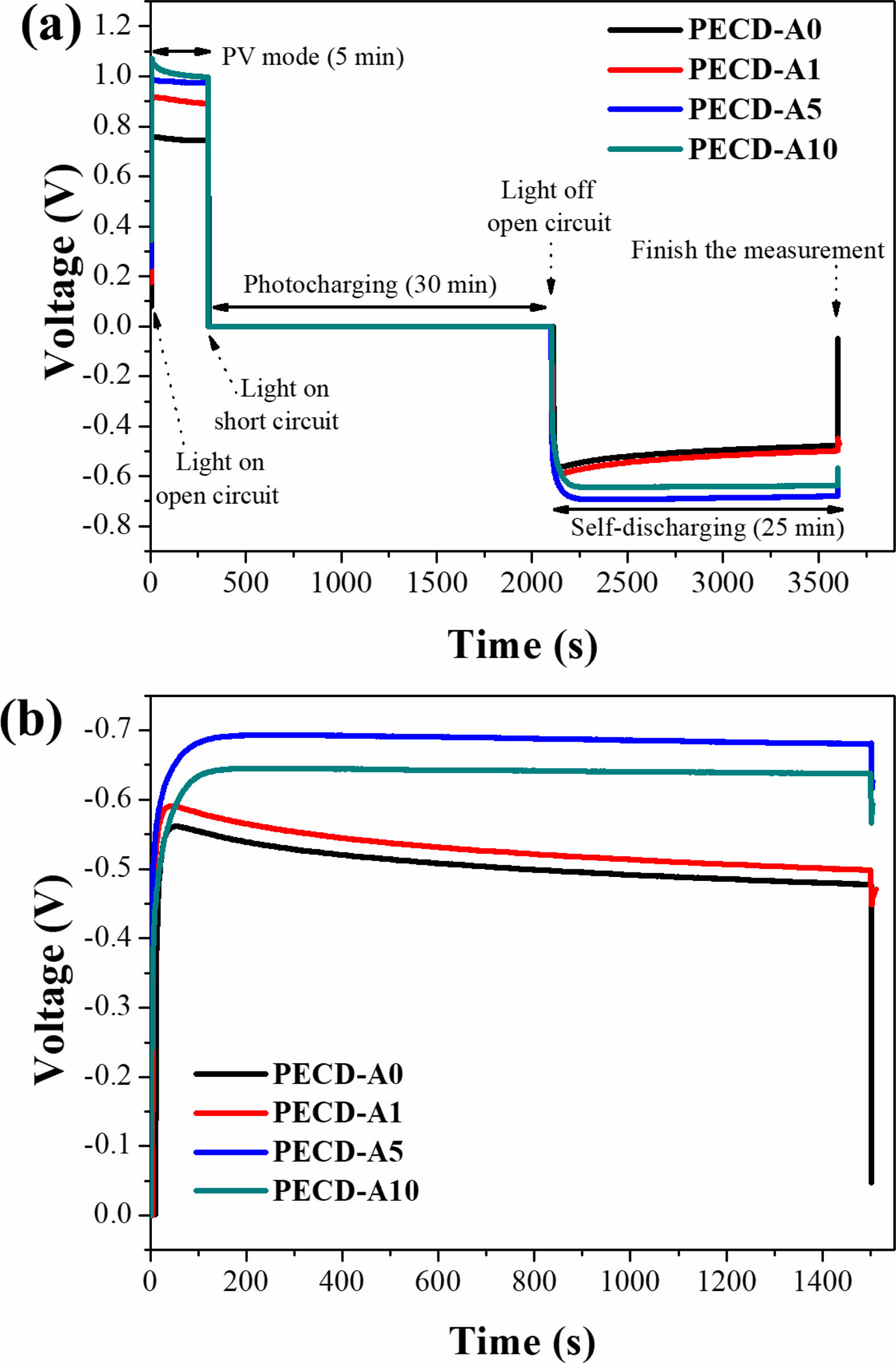
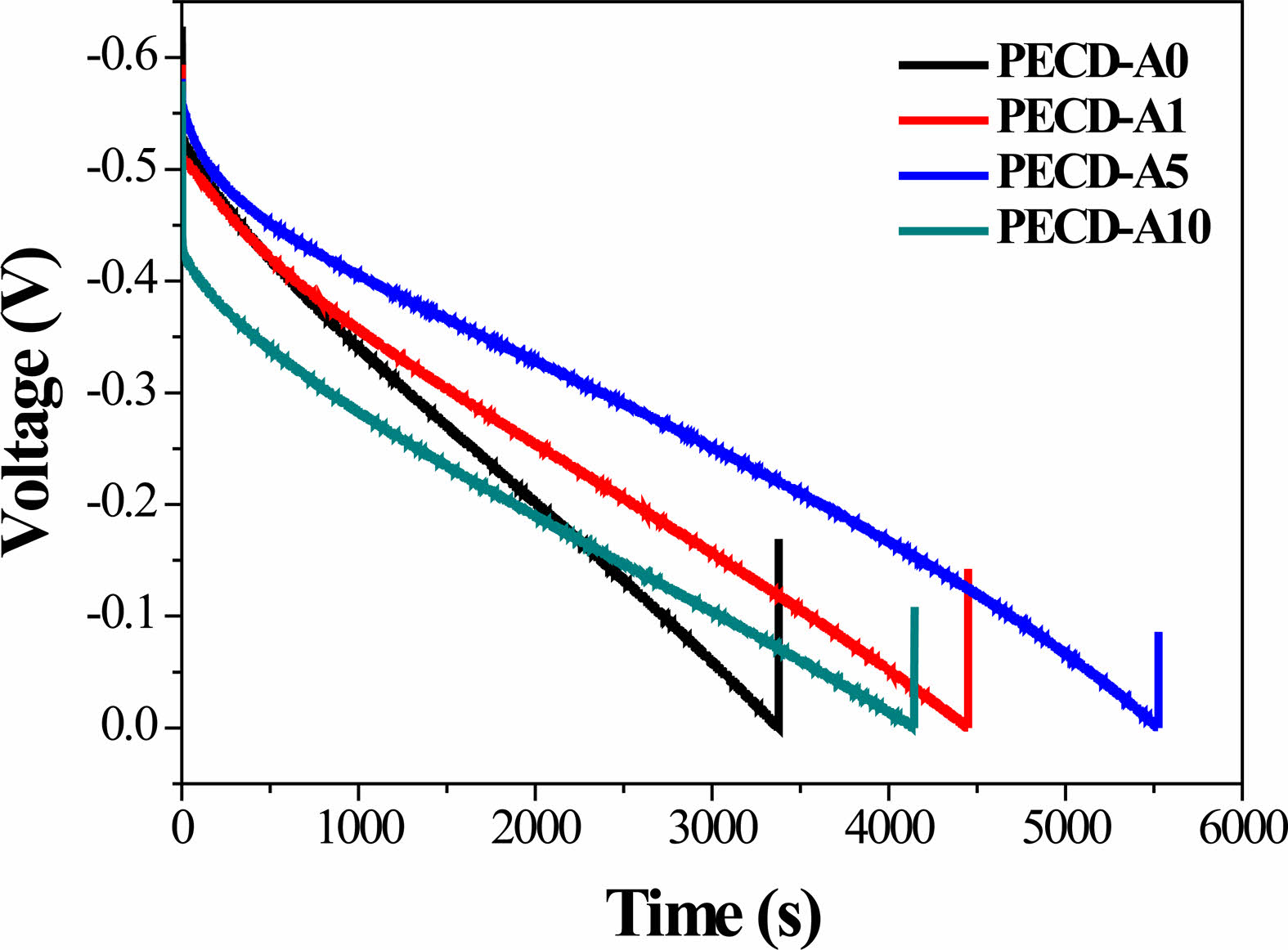
The OCVD method was performed to quantify self-discharge. The change of the voltage in the PECDs was monitored over time according to the illumination and circuit conditions, as shown in Fig. 7a. Just as an external voltage is applied to ECDs, voltage is spontaneously generated in the PECDs under illumination and open circuit conditions (photovoltaic mode). Under illumination and short circuit conditions, the voltage drops and coloring or photocharging occurs. After photocharging, the voltage changes to a negative value under dark field and open circuit conditions because the electric potential of the photoelectrode is lowered than that of the electrochromic electrode.
The photocharged voltage value of the PECDs increased as the number of Al2O3 ALD cycles increased, achieving a maximum value in the PECD-A5 sample; it then decreased in the PECD-A10 sample, as shown in Fig. 7b. This trend is consistent with the change of the ΔT value, as shown in Fig. 6 and Table 2. Meanwhile, the photocharged voltage decreased over time under dark field and open circuit conditions, and this tendency (from the self-discharge phenomenon) decreased as the number of Al2O3 ALD cycles increased.
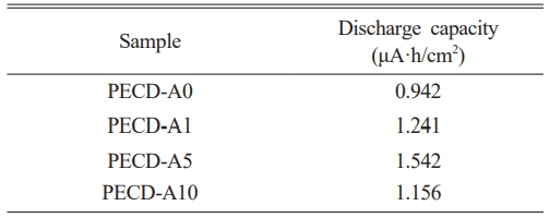
To use the PECD as an energy storage device, a constant voltage must be maintained under the open circuit condition, and current should flow when an external load is applied under the short circuit condition. The galvanostatic discharge curves of the PECDs for different Al2O3 ALD cycles at a fixed current density of 1 μA/cm2 under dark field and short circuit conditions are shown in Fig. 8. The calculated discharge capacities are also listed in Table 3. Similar to the transmittance and OCVD results, the discharge capacity value of the PECDs increased as the number of Al2O3 ALD cycles increased, achieving a maximum value in the PECD-A5 sample, and then it decreased in the PECD-A10 sample. Discharge capacity is proportional to the amount of Li+ ions contained in LixW1-x6+Wx5+O3 and is determined by the number of electrons that flow to the external circuit during discharge. During self-discharge in which electrons are consumed by the reduction of iodine, the discharge capacity decreases. Therefore, the discharge capacity of the PECDs increased via the ALD-deposited Al2O3 layer, which suppressed the self-discharge. However, the PECD-A10 sample with a thick Al2O3 layer exhibited a relatively low discharge capacity due to the slow diffusion rate of Li+ ions.
|
Fig. 1 chematic of the operation mechanism of the PECD in the (a) colored state (photocharging) and (b) bleaching state (discharging). |
|
Fig. 2 XRD patterns of the WO3 thin films with and without a deposited Al2O3 layer and of an ITO substrate as a reference. |
|
Fig. 3 XPS survey spectra of the WO3 thin films with and without a deposited Al2O3 layer. |
|
Fig. 4 HR-SEM images of (a) ITO/glass, (b) a bare WO3 thin film, and (c) a WO3 thin film with a deposited Al2O3 layer (PECD-A10). |
|
Fig. 5 hotocurrent-voltage (J-V) curves of the PECDs fabricated with different numbers of Al2O3 ALD cycles. |
|
Fig. 6 In-situ optical transmittance spectra of the PECDs fabricated with different numbers of Al2O3 ALD cycles. |
|
Fig. 7 The change of the voltage in the PECDs during the open circuit voltage decay (OCVD) analysis: the (a) overall voltage profile and (b) self-discharging region. |
|
Fig. 8 Galvanostatic discharge curves of the PECDs fabricated with different numbers of Al2O3 ALD cycles at a fixed current density of 1 μA/cm2 . |
|
Table 1 Open-circuit voltage (VOC), short-circuit current density (JSC), fill factor (FF), and power-conversion efficiency (η) of the PECDs fabricated with different numbers of Al2O3 ALD cycles. |
|
Table 2 Summary of electrochromic performance parameters measured from the PECDs |
|
Table 3 Discharge capacities of the PECDs in the short circuit condition after photocharging for 30 min under illumination (1 sun). |
To use PECDs not only as ECDs but also as energy storage devices, the photocharged voltage must be constant under dark field and open circuit conditions. We investigated the effects of the deposition of ultra-thin Al2O3 layers via ALD on the electrochromic and self-discharge properties and on discharge capacity. Although the PECDs with Al2O3 layers deposited by ALD showed relatively low J-V performance due to the insulator-type Al2O3, there was no significant hinderance to spontaneous photocharging to color the WO3 electrochromic layer. Based on transmittance and OCVD analysis, ΔT and the photocharged voltage values of the PECDs under illumination and dark field, respectively, increased as the number of Al2O3 ALD cycles increased up to five cycles and then decreased in the PECD-A10 sample due to suppression of iodine reduction at the interface between the electrolyte and WO3 layer. Namely, self-discharging was prevented by deposition of the ultra-thin Al2O3 layer. Battery-mode analysis confirmed that the discharge capacity of the PECDs with an Al2O3 layer deposited by ALD increased due to suppression of self-discharge. However, with the PECD-A10 sample, which had a thick Al2O3 layer of about 1 nm, the values of ΔT, photocharged voltage, and discharge capacity are relatively low due to the slow diffusion rate of Li+ ions.
This paper was supported by research funds of Jeonbuk National University in 2023. This work was also supported by Korea Institute of Energy Technology Evaluation and Planning (KETEP) grant funded by the Korea government (MOTIE) (20213030040110). This work was supported by the Commercialization Promotion Agency for R&D Outcomes (COMPA) grant funded by the Korean Government (Ministry of Science and ICT,2023) (RS-2023-00304743).
Woon-Yong Park: Investigation, Data curation, Formal analysis, Validation, Writing - original draft. Yoon-Tae Park: Data curation, Formal analysis. Byung Guk Ahn: Funding acquisition, Investigation, Supervision, Validation, Writing - review and editing. Ki-Tae Lee: Conceptualization, Funding acquisition, Investigation, Methodology, Supervision, Validation, Writing - original draft, Writing - review and editing.
The authors have no conflicts of interest to declare. All co-authors have seen and agree with the contents of the manuscript and there is no financial interest to report. We certify that the submission is original work and is not under review at any other publication.
The data that support the findings of this study are available from the corresponding author upon reasonable request.
- 1. S. Wang, W. Fan, Z. Liu, A. Yu, and X. Jiang, J. Mater. Chem. C 6 (2018) 191-212.
-

- 2. C. Bechinger, S. Ferrere, and A. Zaban, J. Sprague, and B.A. Gregg, Nature 383 (1996) 608-610.
-
- 3. A. Kolay, A. Das, P. Ghosal, and M. Deepa, ACS Appl. Energy Mater. 1 (2018) 4084-4095.
-
- 4. A. Dokouzis, D. Zoi, and G. Leftheriotis, Mater. 13[11] (2020) 2565.
-
- 5. A. Cannavale, F. Martellotta, F. Fiorito, and U. Ayr, Energies 13[8] (2020) 1929.
-
- 6. Z. Tong, Y. Tian, H. Zhang, X. Li, J. Ji, H. Qu, N. Li, J. Zhao, and Y. Li, Sci. China Chem. 60 (2017) 13-37.
-
- 7. K.-W. Kim, T.Y. Yun, S.-H. You, X. Tang, J. Lee, Y. Seo, Y.-T. Kim, S.H. Kim, H.C. Moon, and J.K. Kim, NPG Asia Mater. 12 (2020) 84.
-
- 8. D.S. Choi, S.H. Han, H. Kim, T.Y. Kim, S.H. Rhyu, D.H. Yoon, and W.S. Yang, J. Ceram. Pro. Res. 15[5] (2014) 273-276.
-
- 9. D. Ma, G. Shi, H. Wang, Q. Zhang, and Y. Li, J. Mater. Chem. A 1 (2013) 684-691.
-
- 10. B.-R. Koo and H.-J. Ahn, Nanoscale 9 (2017) 17788-17793.
-
- 11. W.-Q. Wang, X.-L. Wang, X.-H. Xia, Z.-J. Yao, Y. Zhong, and J.-P. Tu, Nanoscale 10 (2018) 8162-8169.
-
- 12. L. Wang, Y. Liu, G. Han, and H. Zhao, Sol. Energy Mater. Sol. Cells 250 (2023) 112053.
-
- 13. T.D. Nguyen, L.P. Yeo, D. Mandler, S. Magdassi, and A. I.Y. Tok, RSC Adv. 9 (2019) 16730-16737.
-
- 14. M.A. Arvizu, H.-Y. Qu, U. Cindemir, Z. Qiu, E.A. Rojas-González, D. Primetzhofer, C.G. Granqvist, L. Österlund, and G.A. Niklasson, J. Mater. Chem. A 7[6] (2019) 2908-2918.
-
- 15. B.-R. Koo, M.-H. Jo, K.-H. Kim, and H.-J. Ahn, NPG Asia Mater. 12 (2020) 10.
-
- 16. V.H.V. Quy, I.-R. Jo, S.-H. Kang, and K.-S. Ahn, J. Ind. Eng. Chem. 94 (2021) 264-271.
-
- 17. B.-R. Koo, M.-H. Jo, K.-H. Kim, and H.-J. Ahn, Chem. Eng. J. 424[51] (2021) 130383.
-
- 18. Y.-T. Park and K.-T. Lee, J. Ceram. Pro. Res. 14[5] (2013) 632-635.
-
- 19. D. Guan, J. Li, X. Gao, and C. Yuan, RSC Adv. 4 (2014) 4055-4062.
-
- 20. C.-S. Kim, K. Kim, and C.-W. Yi, J. Ceram. Pro. Res. 16[2] (2015) 232-236.
-
- 21. M.A. Kanjwal, N.A.M. Barakat, F.A. Sheikh, G.G. Kumar, D.K. Park, and H.Y. Kim, J. Ceram. Pro. Res. 11[4] (2010) 437-442.
-
- 22. H. Liao, B. Huang, Y. Cui, H. Qin, X. Liu, and H. Xu, J. Energy Storage 55 Part A (2022) 105431.
-
- 23. W.G. Buxton, S.G. King, and V. Stolojan, Energy. Environ. Mater. 6 (2023) e12363.
-
- 24. J. Castillo-Saenz, N. Nedev, B. Valdez-Salas, M. Curiel-Alvarez, M. I. Mendivil-Palma, N. Hernandez-Como, M. Martinez-Puente, D. Mateos, O. Perez-Landeros, and E. Martinez-Guerra, Coatings 11[10] (2021) 1266.
-
- 25. V. Vandalon and W.M.M. Erwin Kessels, Langmuir 35[32] (2019) 10374-10382.
-
- 26. H. Fukumizu, M. Sekine, M. Hori, and P.C. McIntyre, Jpn. J. Appl. Phys. 59 (2020) 016504.
-
- 27. J. Lee, S. Shin, S. Kwon, W. Jang, H. Choi, H. Park, N. Lee, and H. Jeon, J. Ceram. Pro. Res. 22[3] (2021) 253-257.
-
- 28. Y.-T. Park and K.-T. Lee, Opt. Mater. 121 (2021) 111577.
-
- 29. W.Y. Park and K.-T. Lee, J. Ceram. Pro. Res. 22[5] (2021) 584-589.
-
 This Article
-
2024; 25(1): 34-40
Published on Feb 29, 2024
- 10.36410/jcpr.2024.25.1.34
- Received on Oct 4, 2023
- Revised on Nov 21, 2023
- Accepted on Nov 23, 2023
Services
- Abstract
introduction
experimental procedure
results and discussion
conclusions
- Acknowledgements
- Author Contributions
- Conflict of Interest
- Data availability statement
- References
- Full Text PDF
Shared
Correspondence to
- Byung Guk Ahn a,b and Ki-Tae Lee a,b,c,d
-
aDivision of Advanced Materials Engineering, Jeonbuk National University, Jeonbuk 54896, Republic of Korea
bHydrogen and Fuel Cell Research Center, Jeonbuk National University, Jeonbuk 54896, Republic of Korea
cDepartment of Energy Storage/Conversion Engineering of Graduate School (BK21 FOUR), Jeonbuk National University, Jeonbuk 54896, Republic of Korea
dDepartment of JBNU-KIST Industry-Academia Convergence Research, Jeonbuk National University, Jeonbuk 54896, Republic of Korea
Byung Guk Ahn : Tel : +82-63-270-2300 Fax: +82-63-270-2386
Ki-Tae Lee : Tel : +82-63-270-2290 Fax: +82-63-270-2386 - E-mail: bkahn@jbnu.ac.kr, ktlee71@jbnu.ac.kr
Clean-Energy Research Institute(CRI), Hanyang University, 222, Wangsimni-ro, Seongdong-gu, Seoul, 04763, Korea
E-mail: jcpr@hanyang.ac.kr