


- Forming a thick CdZnTe epitaxial film by sublimating closely spaced
Xiang-Xiang Luoa,b*, Cheng-Fang Qiaoa, Simon R Hallb and Chun-Sheng Zhoua,*
aCollege of Chemical Engineering and Modern Materials, Shangluo University, China
bSchool of Chemistry, University of Bristol, UKThis article is an open access article distributed under the terms of the Creative Commons Attribution Non-Commercial License (http://creativecommons.org/licenses/by-nc/4.0) which permits unrestricted non-commercial use, distribution, and reproduction in any medium, provided the original work is properly cited.
Thick Cadmium zinc telluride epitaxial films were grown on (100)GaAs substrate by Close-Spaced Sublimation. The growth rate was around 1 μm/min. SEM observations and XRD θ-2θ scan and ф scan revealed well-defined epitaxial features of the films. The films were found to be polycrystalline at the early stage of growth. As growth progressed, the films gradually became oriented until an epitaxial layer was formed. The polycrystalline to monocrystalline transition was achieved by preferential lateral growth of the grains and with the aid of migration of atoms in the film. This growth mode differs from the well-established epitaxy where a suitable lattice fit is expected from the early stages of film growth. This mode can better guide the growth mode of CZT thick films, and can grow large volume and high-quality thick films. High quality thick films can be better applied in fields such as solar cells, infrared and ultraviolet detection, and X-ray detection.
Keywords: cadmium zinc telluride, epitaxial film, close-spaced sublimation, thick film
The II-VI compound semiconductor, Cd1-xZnxTe, is an important material for radiation detector applications due to its high atomic number, resulting in superior sensitivity and large bandgap allowing room temperature operation, As an II-VI compound semiconductor with excellent photoelectric properties, CdZnTe (CZT) is widely used in medical imaging, industrial nondestructive testing, space exploration, astrophysics and other fields. Cd1-xZnxTe films have been the focus of much research in the fabrication of large area radiation detectors for medical imaging [1], as an alternative to expensive and size-limited bulk crystals, With the development of large-area imaging detectors, the size requirements of CZT crystal for high-performance devices are also increasing. Significant thickness is required for effective absorption. For example, a 10-20 μm thick CdTe layer is required for absorption of 8-20 keV X-rays [2], At present, the mature melt method is commonly used to grow CZT single crystal, but the yield and production efficiency of this method are low, which increases the cost and price of CZT crystal and limits its application [3]. The growth of both polycrystalline and epitaxial films has been studied. However, even if CZT epitaxial film has a wide market prospect, it cannot avoid the formation of a large number of defects in the growth process [4], which seriously affects the photoelectric properties and carrier transport properties [5]. Epitaxial films offer better performance by eliminating the negative influence of grain boundaries. In addition, Cd1-xZnxTe is the main substrate for the growth of HgCdTe (MCT) epilayers because it allows a total chemical and crystalline compatibility. It is used in infrared focal plane array detectors [6]. High quality thick films can be better applied in fields such as solar cells, infrared and ultraviolet detection, and X-ray detection.
Here we present the growth of CdZnTe epitaxial films on (100)GaAs substrates. This is achieved by a simple process called Close-Spaced Sublimation (CSS). First proposed by Nicoll [7] in 1963, the idea of growing epitaxial semiconductor films by CSS was widely accepted. Subsequently, due to its cost effectiveness and, in particular, the excellent photovoltaic performance of the resulting cells, this method has been recognised as an excellent approach for growing polycrystalline CdTe films for solar cells. CSS has the advantages of a high growth rate, no need for a hard vacuum and a much simpler experimental setup than other epitaxial techniques, especially for thick film growth. For single crystal growth, either a powder or a wafer source can be used. This technique has been used to grow epitaxial thick films such as SiC and AlN [8]. Studies on the growth of II-VI compound semiconductor films have been carried out by several groups by modification of the CSS equipment to achieve suitable growth conditions [9], especially a relatively stable growth interface. Mass transfer at the growth interface in the CSS process is very active due to the high growth rate, in the range of several micrometres per minute, which differs from the well-established epitaxial techniques where a stable growth interface is expected. Two-dimensional (2D) layer-by-layer growth is the well-established mechanism for epitaxy [10]. In this paper we show the transition from the polycrystalline film to the epitaxial layer of CdZnTe thick film grown on (100)GaAs by a conventional CSS process [11]. This is indicative of a 3D growth mode [12]. This mode can better guide the growth mode of CZT thick films, and can grow large volume and high-quality thick films [13].
Furthermore, the change mechanism of defects in CZT epitaxial film can be obtained [14], which could guide the growth of CZT epitaxial film [15].
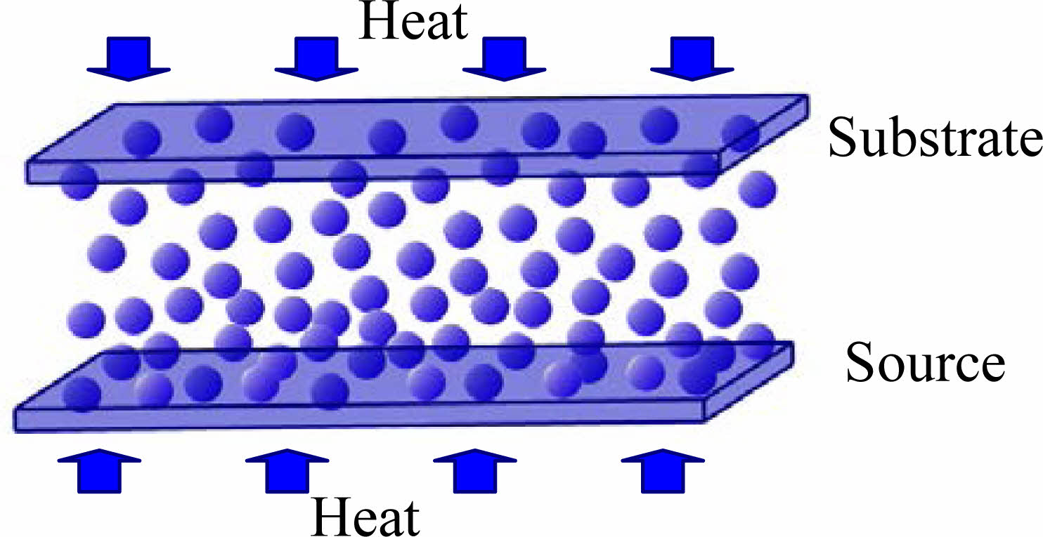
The CSS process is shown schematically in Fig. 1. Cd0.9Zn0.1Te powder was used as the source and (100)GaAs with a 2° orientation towards [110] and an area of 11 × 11 mm2 was used as the substrate. The distance between the source and the substrate was kept at a value of 5 mm. The source and substrate were heated and maintained at 600 °C and 575 °C, respectively, for film deposition after the CSS furnace was evacuated and filled with Ar at a pressure of 100 Pa. Field emission scanning electron microscopy (FE-SEM, Zeiss Supra-55) was used to characterise the morphology of the films. Energy dispersive X-ray spectrometry (EDS, Oxford Inca Energy 350) was used to measure the zinc concentration. Both X-ray θ-2θ scan in the range of 2θ=20°-80° and rotational ф scan for (511) set of planes were performed by synchrotron radiation X-ray diffraction to clarify the structural properties of the grown films. This was carried out at the National Synchrotron Radiation Laboratory of China.
|
Fig. 1 Schematic showing the CSS procedure. |
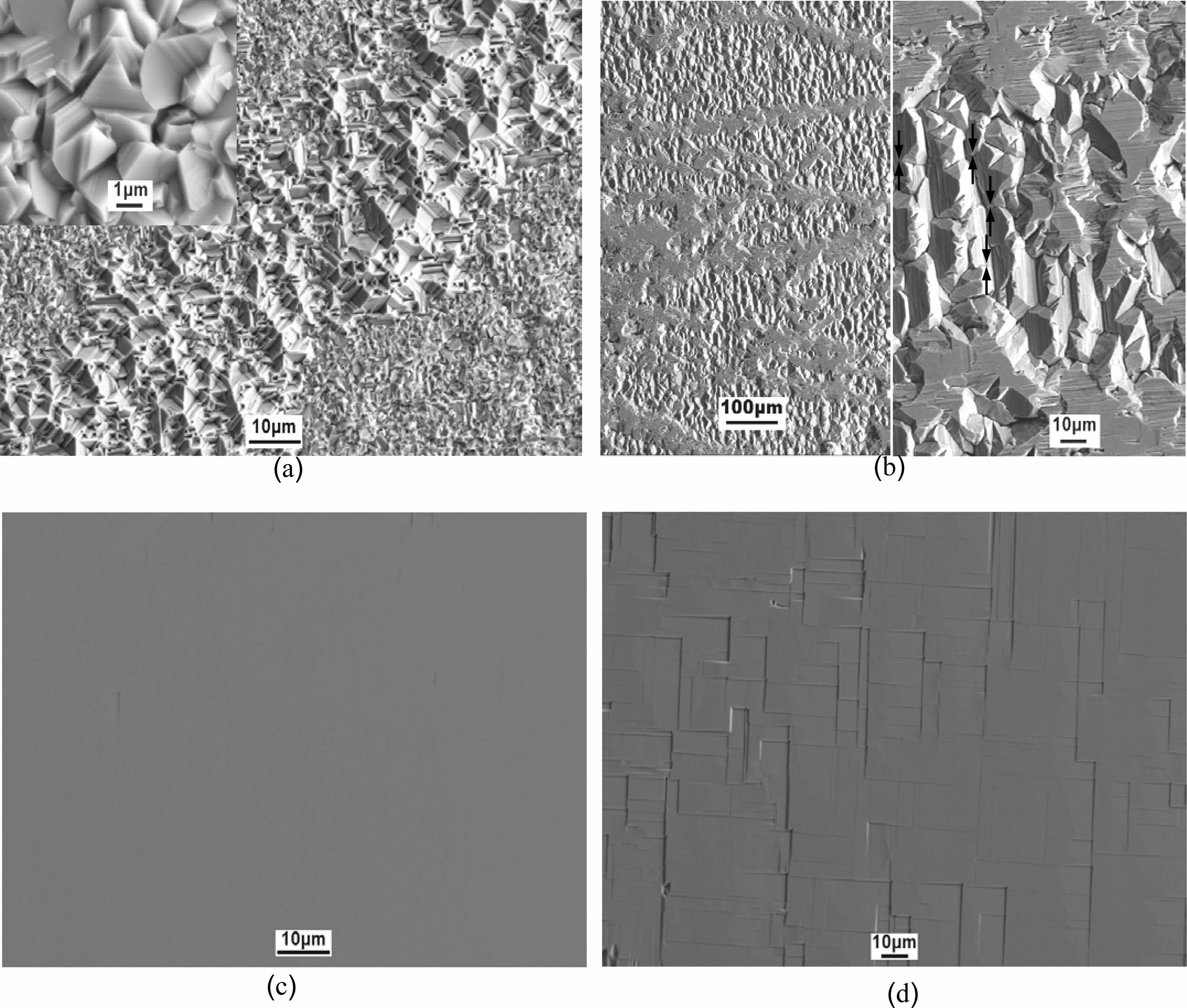
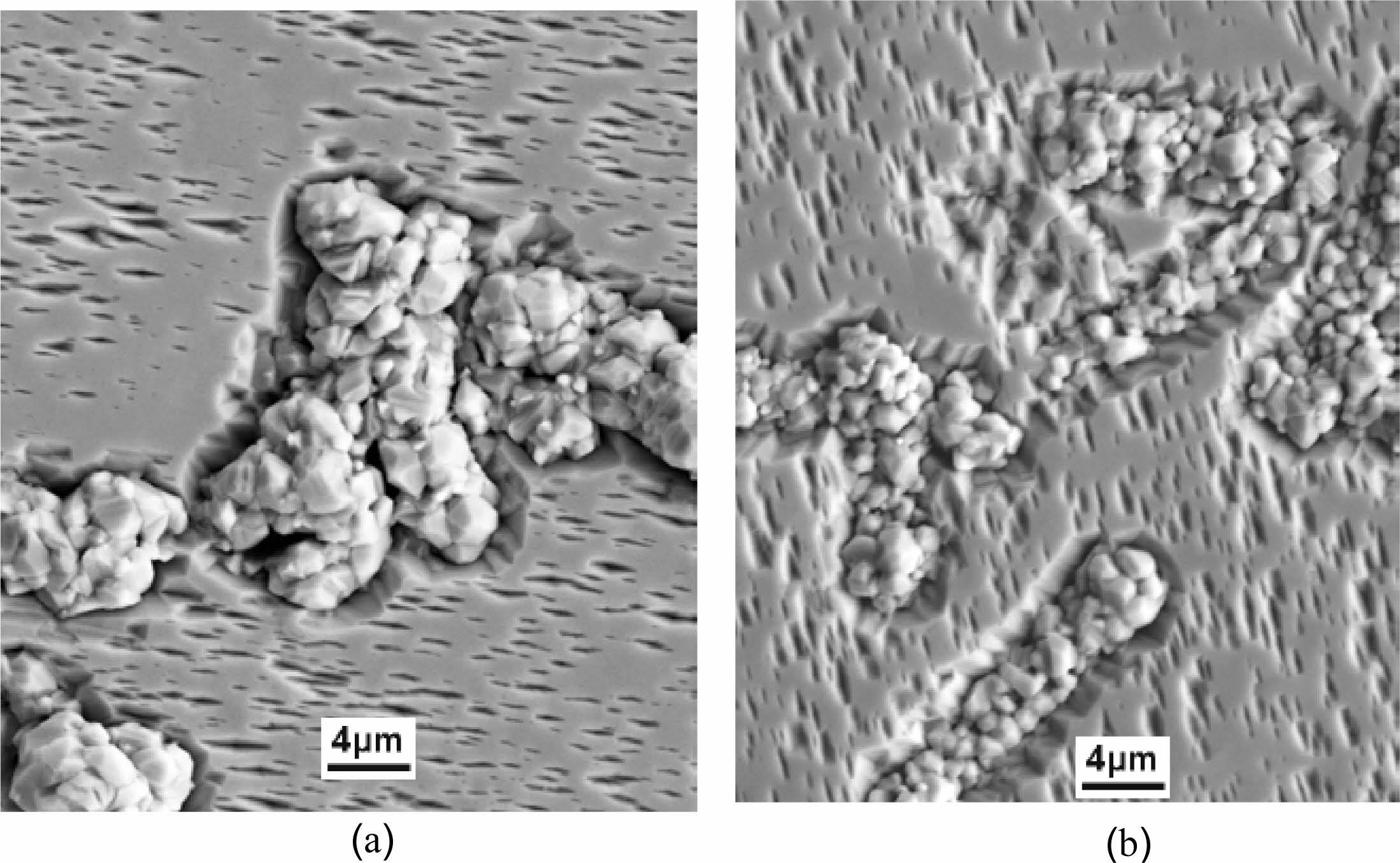
Figure 1 shows the FE-SEM images of CdZnTe films on GaAs (001) substrates grown for 11 minutes (Fig. 2(a)), 20 minutes (Fig. 2(b)) and 30 minutes (Fig. 2(c) and (d)), respectively. When the growth time was 10 min, it was found that pyramid structure bands were present on the film surface as shown in Fig. 2(a) and the film consisted mainly of platelet-shaped grains as shown in the inset of Fig. 2(a). The pyramidal morphology was developed from the platelet-shaped grains as shown in Fig. 2(a). A similar pyramidal structure on the edge of an epitaxial GaAs layer on (111)Ge was also observed by Nicoll [10], the pioneer of the CSS technique. It can be speculated that the pyramidal structure is a form of poor epitaxy. The atoms in the film are able to rearrange during growth to adopt a lower energy orientation.
The surface morphology shown in Fig. 2(b) was obtained after 20 min of growth with elongated polyhedra and crisscrossed bands. The right image is an enlargement of the left image. It shows that the polyhedral grains are aligned and the bands appear to be formed by flattened and coalesced grains. Grain boundaries are on the verge of disappearing, as indicated by the head-to-head arrows. By further increasing the growth time to 30 min, CdZnTe films without grain boundaries were obtained, as shown in Fig. 2(c). The orthogonal lines in Fig. 2(d) are growth steps observed at the edge of the CdZnTe film. They reflect the cubic crystal structure of the GaAs substrate. Zn was almost undetectable within the precision of EDS in the 10 min growth film. It had an x value of 0.4 in the 30 min growth Cd1-xZnxTe film. Due to the significantly lower vapour pressure of Zn compared to Cd in this non-congruently sublimated ternary compound, a lateral Zn gradient was expected.
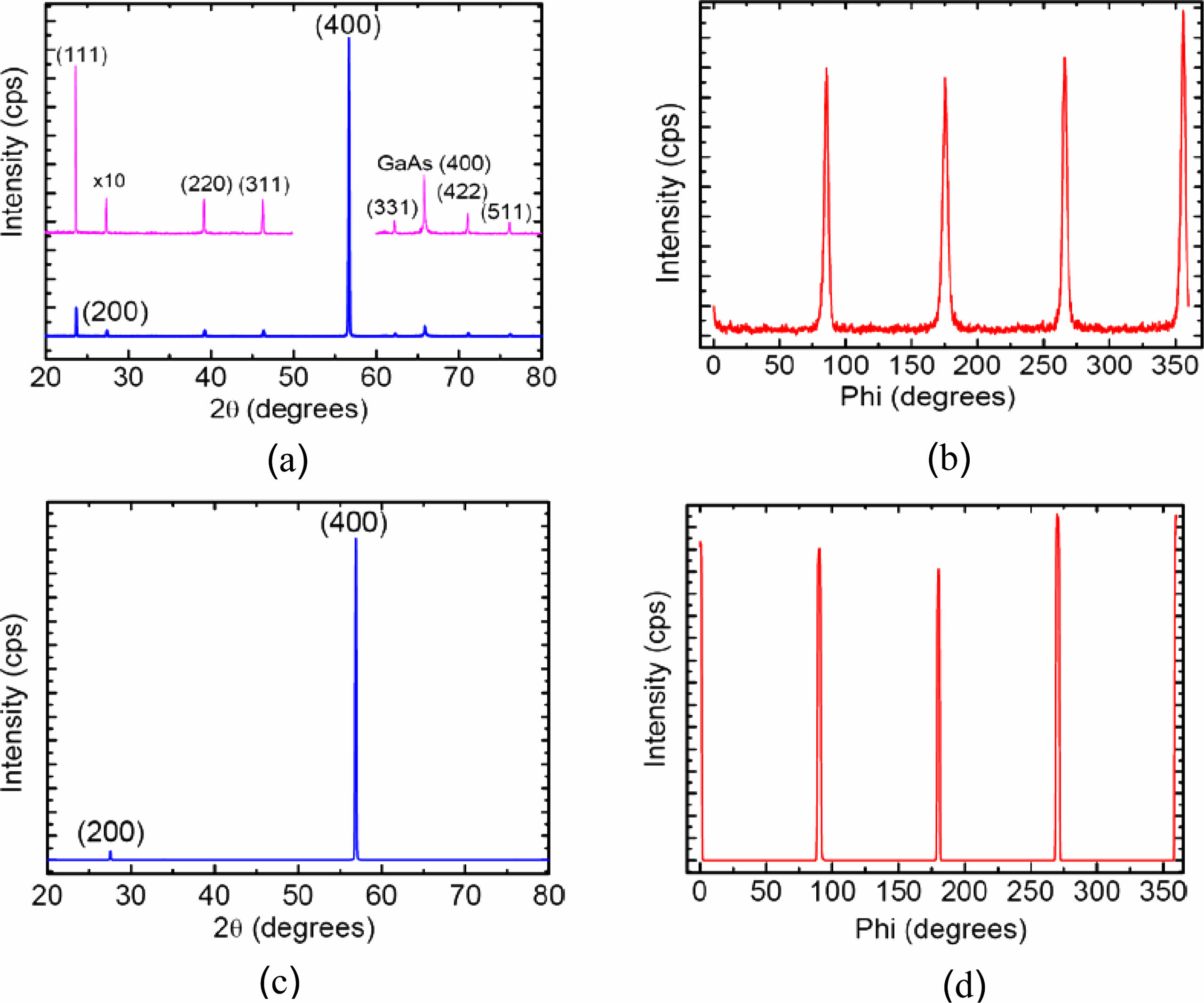
Figure 3 shows the synchrotron X-ray diffraction spectra of CdZnTe films by both θ-2θ scanning and rotational ф scanning of the (511) set of reflections. The θ-2θ spectrum of the CdZnTe film grown for 10 min shown in Fig. 3(a) has all normal diffraction in the range of 20°~80° (see PDF map 15-0770) and a strong (400) diffraction peak, indicating a polycrystalline film with an intense (400) texture, which is consistent with the observation from the FE-SEM images shown in Fig. 2(a). The (400) diffraction from the GaAs substrate is also observed. Four 90° separated diffraction peaks are observed by ф-scan of the (511) diffraction set, as seen in Fig. 3(b), indicating that the film has fourfold symmetry, which is consistent with the cubic crystal structure, and therefore implies that the platelet-shaped grains shown in Fig. 2(a) have the same in-plane orientation.
The XRD spectra of the CdZnTe film grown(JCPDS No.15-0770) for 35 min are shown in Fig. 3(c) and Fig. 3(d). There are only two reflections corresponding to the (002) and (004) planes of zinc blende CdZnTe in the θ-2θ XRD spectrum in Fig. 3(c). No diffraction from (100)GaAs was observed. This is because the film is too thick (about 30 μm) for the X-rays from the substrate to pass through. A 360° ф scan of (511) planes shows four equally spaced peaks, indicating in-plane orientation. This is shown in Fig. 3(d). This confirms the perfect orientation of the film both out of the plane and in the plane.
The analysis of SEM and XRD results of CdZnTe films grown for different times shows that the CdZnTe film grown on (100)GaAs by CSS is polycrystalline. In the early stage it is in-plane oriented. The polycrystalline film evolves into an epitaxial layer as growth continues. Nucleation, routine grain growth by coarsening, grain coalescence and film smoothening are all involved in the growth of the CdZnTe epitaxial layer. The last three processes should occur simultaneously, according to the facts that: (i) the film grown for 10 min was partially epitaxial, as indicated by the pyramidal structured area in Fig. 2(a), whereas it was mostly polycrystalline; (ii) an analogous situation occurred when the growth time was increased to 20 min, except that the epitaxial area broadened, as indicated by the cross bands in Fig. 2(b); (iii) an apparent grain growth is inferred from the fact that the size of the grains in Fig. 2(b) is almost an order of magnitude larger than that in Fig. 2(a).
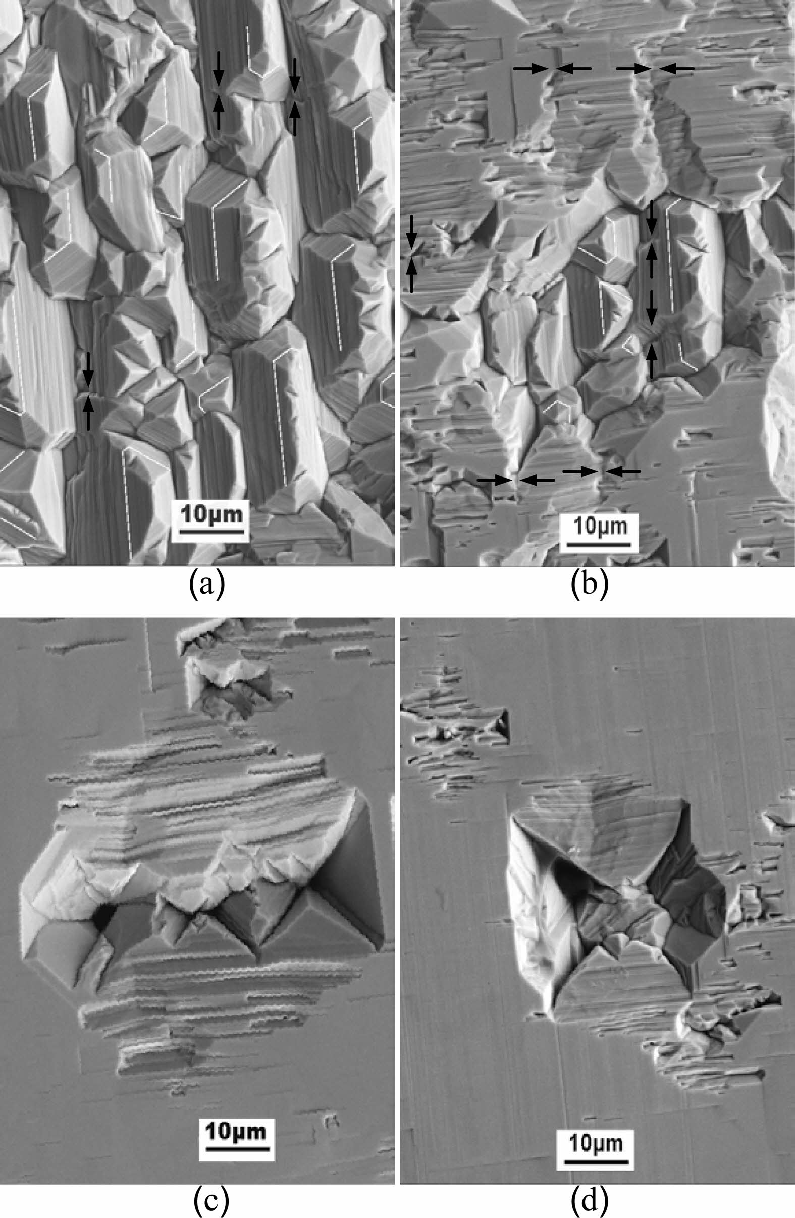
The polyhedral grains have tetrahedral tips and steeply sloping sides in the SEM image in Fig. 4(a). The grains are composed of layers that leave streaks (indicated by lines). The layers are tilted clockwise or counterclockwise at almost the same angle with respect to the film surface. The layers are most likely (111) planes, on the basis of observations that most grains are tilted with normal tetrahedrons and (111) produces the most intense diffraction peak other than (400) in the θ-2θ XRD spectrum (Fig. 3(a)) for the early stage CdZnTe film. In fact, except that in the latter case the grains are randomly arranged rather than aligned, the grains shown in Fig. 4(a) are similar in appearance to the grains of (111) textured polycrystalline CdTe films grown by CSS [12, 18]. Lateral growth is realised because (111) atomic layers can expand by adding atoms in all planar directions. The disappearance of the boundary (indicated by the arrows from head to head) on some grains indicates that these grains are coarse by the coalescence of several smaller grains. Coalescence between two adjacent grains requires lattice matching at the atomic level. This could be achieved by expansion of the (111) layers and migration of atoms in the grains. Since the CdZnTe film is always in-plane, lattice matching can be achieved by simple layer expansion of each grain, as shown in Fig. 3(b) & (d).
The slopes of the grains in the centre of the image in Fig. 4(b) are much less steep and the tetrahedral peaks do not show any visible differences compared to those in Fig. 4(a), suggesting that the slopes of each grain grow laterally. The FE-SEM images of the growth pits in the CdZnTe film during its development to a smooth layer are shown in Fig. 4(c) and Fig. 4(d). All the tetrahedral peaks are below the film surface. This is further evidence of the lateral growth of the grains. The lateral growth raises the low area of the film surface to obtain a smooth surface.
An analogous pit in Fig. 4(b) can develop into the growth pit shown in Fig. 4(d). Grain boundaries are clear in Fig. 4(a) and vague in the coalesced region surrounding the polyhedral grains in Fig. 4(b). They are absent in the region surrounding the pits in Fig. 4(c) and Fig. 4(d). This suggests that preferential lateral growth promotes grain coalescence and smoothing of the CdZnTe film, as evidenced by the evolution of the morphology from Fig. 4(a) to Fig. 4(d). The bottom edge of the small triangle marked in red line in Fig. 4(c) is approximately 10 microns.
Migration of atoms in the film also plays an important role in epitaxial growth, in addition to preferential lateral growth. The migration was recognised by the pyramidal structure observed in Fig. 2(a) and confirmed by annealing a heavily flawed sample with growth pits filled with agglomerated small crystals as shown in Fig. 5. From Fig. 5(a) and Fig. 5(b) it can be seen that the agglomerates shrank and coalesced into the matrix of the film after annealing. This indicates the ability of the atoms in the film to migrate. Since the annealing conditions were deliberately set to be the same as the growth conditions of this sample, the atoms in the film are able to migrate during growth to also achieve a more energetically favourable atomic arrangement [16]. This migration could have the effect of smoothing out the rough surface of the film and also the effect of bringing the atoms into a more uniform orientation with respect to the substrate and to each other [17]. This migration phenomenon can be related to the Orientation Attachment (OA) growth mechanism. OA is defined as the spontaneous self-organisation of adjacent particles to share a common crystallographic orientation, followed by the attachment of these particles at a planar interface. OA has been extensively studied by Penn et al. [9]. It is a robust approach to single nanocrystal growth [18].
It is therefore concluded that the lateral growth, which is realised by the expansion of the sub-layers of each grain, together with the atomic migration, smoothens the film surface and promotes the formation of the epitaxial CdZnTe film.
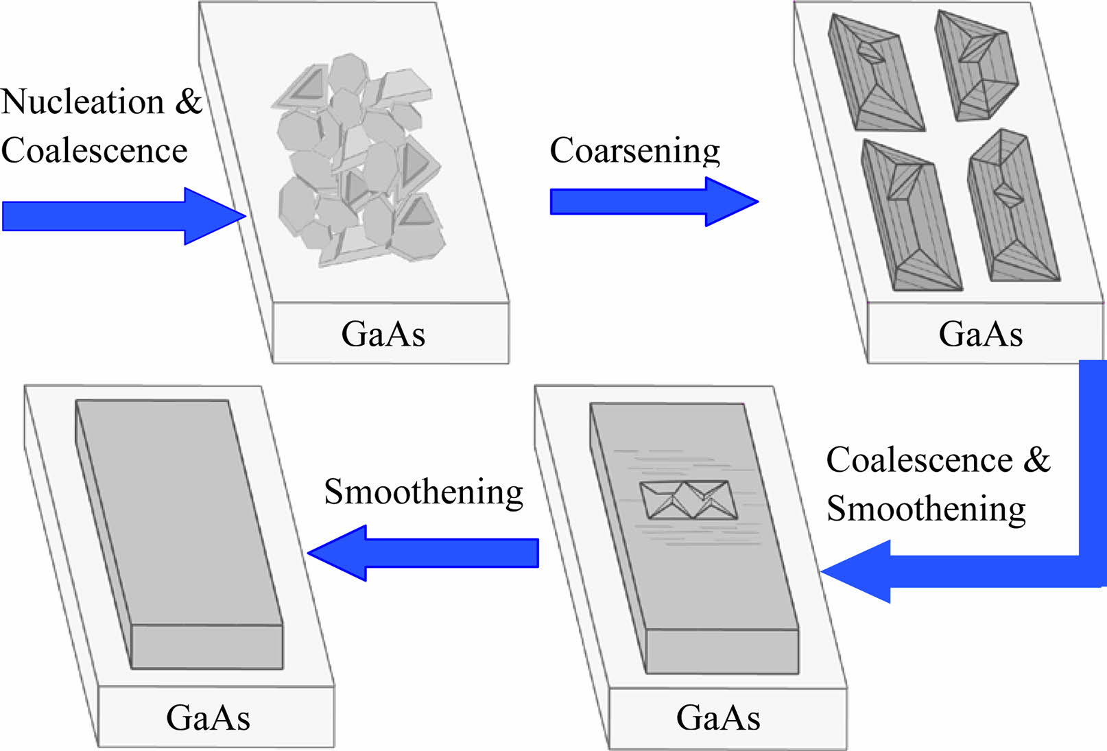
The evolution of the CdZnTe film from polycrystalline to monocrystalline by preferential lateral growth and migration of atoms in the film is shown schematically in Fig. 6. Through nucleation and subsequent coalescence, a continuous film of platelet-shaped small crystals is formed. Small crystals coarsen into large grains with layered structures as growth proceeds. Coarsening involves both 3D growth and coalescence of small crystals, with the coalescence trace left on each individual grain. The film is still polycrystalline at this stage. As growth continues, the grains coalesce and the low-lying areas of the film are leveled by preferential lateral growth and atomic migration, forming a smooth epitaxial layer. Grain coalescence and film smoothing could be promoted by both lateral growth and atomic migration. In the transition from polycrystalline to monocrystalline, the former is expected to play the major role. Throughout the growth process, the transition from polycrystalline to epitaxial film occurs.
In other systems, epitaxial films with early polycrystalline stages have also been observed. Bi4Ti3O12 single crystalline films have been grown on (001)SrTiO3 substrate via a vapour-liquid-solid process by Takahashi et al., which involves dissolving an impurity species in a liquid flux layer deposited on the film/substrate surface and crystallising supersaturated species in the solid film under a quasi-equilibrium state between the growing film and the liquid flux. In (111)CdTe film deposition on (100)Si substrate, films with single crystal character were obtained by overgrowth of the dominant (111) domains formed at the early stage of growth. The domains with other orientations remained at the interface in the final product [19]. The growth mode observed in the present study differs from these approaches, along with OA [20]. As growth progressed, the films gradually became oriented until an epitaxial layer was formed. The polycrystalline to monocrystalline transition was achieved by preferential lateral growth of the grains and with the aid of migration of atoms in the film. This growth mode differs from the well-established epitaxy where a suitable lattice fit is expected from the early stages of film growth.
|
Fig. 2 FE-SEM images of CdZnTe films on (100)GaAs substrates grown for different times: (a) 10 min, the inset shows the morphology of most of the area; (b) 20 min, the head-to-head arrows indicate the disappearance of grain boundaries; 30 min (c) the morphology of most of the area and (d) the growth steps at the edge of the film. |
|
Fig. 3 Synchrotron X-ray diffraction spectraof CdZnTe films grown for (a) 10 min and (c) 30 min by θ-2θ scan, (b) 10 min and (d) 30 min by rotating ф scan of the (511) diffraction set. |
|
Fig. 4 FE-SEM images of a CdZnTe film grown for 30 min to illustrate the process of smoothing and coalescence: (a) elongated polyhedral grains; (b), (c) and (d) after smoothing. The analogous morphology shown in (b) should develop into the growth pit shown in (d). The white lines guide the eye to the grain layers. The head-to-head arrows indicate the disappearance of grain boundaries. |
|
Fig. 5 FE-SEM images of a CdZnTe film before (a) and after (b) annealing, showing the possibility of atoms migrating during growth. The annealing conditions were deliberately set to match the growing conditions. |
|
Fig. 6 Schematic diagram showing the evolution of the CdZnTe film from a polycrystalline to an epitaxial layer. The grains are detached for visual convenience. In reality, they should stick together. During the coalescence and smoothening of the four grains shown in the second step, the pit shown in the third step with four tips below the film surface is formed. |
Thick single crystalline (100)CdZnTe films have been grown on (100)GaAs substrates by CSS. This technique is characterised by its fast growth rate and high cost effectiveness. At the early stage of growth, small platelet-shaped crystals were observed. Then, through a typical coarsening process and increased surface smoothness, these platelets developed into large grains. As the growth continued, the grain boundaries disappeared. A perfectly oriented epitaxial layer was obtained. The preferential lateral growth of the layered grains and the migration of atoms in the film completed the transition from polycrystalline to monocrystalline. This mode of growth is different from that of well-defined epitaxy, where a fine lattice adjustment is expected at the early stage of the growth of the film. High quality thick films can be better applied in fields such as solar cells, infrared and ultraviolet detection, and X-ray detection.
This work was supported by the National Natural Science Foundation of China (Grant No. 22173056)(No.22003037), Shaanxi Province Innovation Talents Promotion Plan - Young Science and Technology Nova Project (2020KJXX-085), Shaanxi Provincial Education Department Key projects (22JS015), Shaanxi Provincial Shangluo city Science and Technology Bureau Project (2022-Z-0036) (2022-J-0005), and Shaanxi Provincial Shangluo city Shangluo University Doctor’s Fund (20SKY006).
- 1. T.E. Schlesinger, J.E. Toney, H. Yoon, E.Y. Lee, B.A. Brunett, L. Franks, and R.B. James, Mat. Sci Eng. R. 32[4-5] (2001) 103-189.
-

- 2. M. Niraula, K. Yasuda, R. Torii, R. Tamura, Y. Higashira, and Y. Agata, J. Electron Mater. 48[12] (2019) 7680-7685.
-
- 3. S. Wu, Z. Huang, B. Chen, X. Liu, Y. Ma, Y. Huang, S. Tang, C. Liang, and W. Liu, Mater Charact. 185 (2022) 111739.
-
- 4. X. Luo, G. Zha, L. Xu, and W. Jie, Sensors. 19[3] (2019).
-
- 5. G. Sato, T. Fukuyama, S. Watanabe, H. Ikeda, M. Ohta, S.n. Ishikawa, T. Takahashi, H. Shiraki, and R. Ohno, Nucl. Instrum. Methods Phys. Res. Sect. A. 652[1] (2011) 149-152.
-
- 6. A. Cola, I. Farella, N. Auricchio, and E. Caroli, J. Opt. A:Pure. Appl. Opt. 8[7] (2006) S467.
-
- 7. R.E. Meredith and C.W. Tobias, J. Electrochem. Soc. 110[12] (1963) 365-370.
-
- 8. R. Yakimova, A. Kakanakova-Georgieva, G.R. Yazdi, G.K. Gueorguiev, and M. Syvaejaervi, J. Cryst. Growth. 281[1] (2005) 81-86.
-
- 9. J. Aguilar-Hernandez, G. Contreras-Puente, A. Morales-Acevedo, O. Vigil-Galan, F. Cruz-Gandarilla, J. Vidal-Larramendi, A. Escamilla-Esquivel, H. Hernandez-Contreras, M. Hesiquio-Garduno, and A. Arias-Carbajal, Semicond. Sci. Tech. 18[2] (2003) 111-114.
-
- 10. R.L. Penn and J.F. Banfield, Am. Mineral. 83[9-10] (1998) 1077-1082.
-
- 11. U. Rentsennorov, B. Davaabal, B. Dovchin, and JadambaaTemuujin, J. Ceram. Process. Res. 22[2] (2021) 232-239.
-
- 12. T.V. Khai, P.T. Trang, L.N. Long, T.V. Le, and P.T. Mai, J. Ceram. Process. Res. 22[4] (2021) 425-435.
-
- 13. A. Chimento, A. Santarsiero, D. Iacopetta, J. Ceramella, A.D. Luca, V. Infantino, O. Parisi, P. Avena, M. Bonomo, and C. Saturnino, Int. J. Mol. Sci. 22[10] (2021).
-
- 14. R. Srinivasan, B.S. Babu, P. Prathap, R. Whenish, and G.C.F. A, J. Ceram. Process. Res. 22[1] (2021) 16-24.
-
- 15. M. Bugdayci, S. Baslayici, and M.E. Ama, J. Ceram. Process. Res. 22[1] (2021) 98-105.
-
- 16. A.A. Al-Allaq, J.S. Kashan, M.T.I. El-Wakad, and A. Soliman, J. Ceram. Process. Res. 22[4] (2021) 446-454.
-
- 17. X. Luo, F. Li, C. Qiao, F. Yuan, and C. Zhou, Therm. Sci. 27[3 Part A] (2023) 2183-2194.
-
- 18. E.M. Larramendi, E. Puron, and L.C. Hernandez, J. Cryst. Growth. 223[4] (2001) 447-449.
-
- 19. R. Takahashi, Y. Yonezawa, M. Ohtani, M. Kawasaki, K. Nakajima, T. Chikyow, H. Koinuma, and Y. Matsumoto, Adv. Funct. Mater. 16[4] (2006) 485-491.
-
- 20. Y. Xin, N.D. Browning, S. Rujirawat, S. Sivananthan, Y.P. Chen, P.D. Nellist, and S.J. Pennycook, J. Appl. Phys. 84[8] (1998) 4292-4299.
-
 This Article
-
2023; 24(6): 935-940
Published on Dec 31, 2023
- 10.36410/jcpr.2023.24.6.935
- Received on Jun 28, 2023
- Revised on Aug 22, 2023
- Accepted on Aug 30, 2023
Services
- Abstract
introduction
experimental section
results and discussions
conclusions
- Acknowledgements
- References
- Full Text PDF
Shared
Correspondence to
- Xiang-Xiang Luo a,b, Chun-Sheng Zhou a
-
aCollege of Chemical Engineering and Modern Materials, Shangluo University, China
bSchool of Chemistry, University of Bristol, UK
Tel : 08613991149672 Fax: 086 0914-2986027 - E-mail: luo_xiangx@163.com, slzhoucs@126.com
Clean-Energy Research Institute(CRI), Hanyang University, 222, Wangsimni-ro, Seongdong-gu, Seoul, 04763, Korea
E-mail: jcpr@hanyang.ac.kr