


- Effect of annealing temperature on the properties of Cu2O thin films by RF magnetron sputter using Cu/Cu2O as composite targets
Boen Hounga,*, Cho Liang Chunga, Peng Chieh Yeha, Jhih Kai Wua and Wei Lin Yeha
aDepartment of Materials Science and Engineering, I-Shou University, 840 Kaohsiung City, Taiwan
This article is an open access article distributed under the terms of the Creative Commons Attribution Non-Commercial License (http://creativecommons.org/licenses/by-nc/4.0) which permits unrestricted non-commercial use, distribution, and reproduction in any medium, provided the original work is properly cited.
Single phase of Cu2O films were deposited by RF magnetron sputter using composite targets containing Cu2O with 0 and 7 wt % of Cu concentrations, respectively. The films were consequently annealed at temperatures from 250 to 550 oC. XRD results showed a phase transformation from Cu3O4 → CuO → Cu2O for the films with 0 wt % Cu as annealing temperature increasing from room temperature to 350 oC. An enhancement of crystallization of Cu2O phase with annealing temperature was found in both films. FESEM demonstrated the grain sizes of both films increased from approximately 25~35 nm to 100~140 nm as annealing temperatures increasing to 550 oC. The root mean square (Rms) roughness was approximately 14.8 nm at room temperature and increased up to 46.7 nm at annealing temperature of 550 oC for 7 wt % of Cu. As a result, the optimal electrical properties of Cu2O film was obtained, producing a resistivity of 0.19 Ω·cm, a carrier density of 2.25 × 1018 cm-3 and a mobility of 11.2 cm2·V−1·s−1 at annealing temperature of 450 oC. The transmittances s in the visible range was found to decrease with increasing annealing temperature, while the optical band gaps are in the order of 2.45-2.63 eV
Keywords: RF magnetron, annealing temperature, electrical resistivity, mobility
For applications in optoelectronic devices, solar cells and gas sensors, a p-n junction requires a combination of n-type and p-type transparent conducting oxides (TCOs) thin films. Most of the existing TCOs thin films are n-type such as ZnO, In2O3 and In-Ga-Zn Oxides [1-6], whereas binary oxides with p-type conductivity are rather difficult to fabricate. Typical p-type TCOs such as NiO, SnO, ochalcogenides and oxydelafossite Cu-based oxides [7-14] showed either low electrical conductivity or low optical transmittance. For example, CuAlO2 thin films show a 75% of transmittance in the visible region; however, the lower hole concentrations result in low electrical conductivities due to the lack of Cu-O-Cu linkage structure [15]. On other hand, CuCrO2 thin film has an electrical resistivity of 4.5 × 10⁻¹ Ω·cm, but it only exhibits 30% of transmittance [16]. Even though rather new development of oxychalcogenides exhibit greater hole mobility because of their stronger hybridization, but their inherent narrow band gap limits to visible light transparency [17].
Recently, Cu2O, a p-type TCOs, has attracted much attention in solar cell and film transistor applications [18, 19]. There are several reasons Cu2O are chosen for photovoltaic applications. First, Cu2O have abundant non-toxic source materials with a direct band gap of 2.0~2.6 eV [20-23]. Second, Cu2O can be prepared with possibly adjusted by controlling the compositions and processing parameters [24-26]. Chen et al. demonstrated that the structure of Cu2O film can be modified by changing the substrate temperature and oxygen pressure during pulsed laser deposition. The X-ray diffraction data reveals that the structure of the films changes from CuO to Cu2O phase with the decreasing of the oxygen pressure. In addition, the Cu2O preferred orientation of (200) and (111) can be also adjusted by changing substrate temperature. Guzman et al. studied the influence of dopants such as magnesium, manganese and lanthanum on the properties of Cu2O. They found these dopants not only alter the grain size of Cu2O, but also change the optical band gap of Cu2O. Therefore, if a Cu2O solar cell could reach grid parity in mass production, it could rapidly scale to satisfy humanity’s 1000 exajoule energy demand all over the world [27]. However, in literature, p-type Cu2O film is a poor semiconductor with best electrical resistivity around 10-2 Ω·cm [28, 29]. Therefore, to improve the electrical conductivity of Cu2O film is one of main goals in this research area. At present, there are various methods such as thermal oxidation, sol-gel processing, electrodeposition, laser and atomic layer deposition, and magnetron sputtering deposition have been carried out to prepare Cu2O films [30-32]. In magnetron sputtering deposition processing, Cu2O film is generally prepared by Direct-Current (DC) magnetron sputter using metal Cu as a target. As a result, other copper oxide phases such as CuO, and Cu4O3 instead of single Cu2O phase were always present in the films due to the high reactivity between metal Cu target and O2 [33-35]. To solve this problem, CuO target is tried to replace with Cu to produce single Cu2O film. However, a dense CuO target is required to achieve this goal under a complicated production process [36]. Until recently, N2 was found to efficiently supress the presence of the CuO phase and exhibited low resistivity ohmic contacts when N2 gas was added as dopant during sputtering [37, 38].
For practical reason in term of mass production, magnetron sputtering is adopted as a major industrial process because of large-area deposition capability, affordable targets, and high quality films. Consideration of high-volume productions, it often requires magnetron sputtering as a deposition method. The challenge for the manufacturers is to achieve good sputtering efficiency and excellent properties of thin films. These factors are strongly dependent on the properties of the sputtering targets such as purity, density and homogeneity [39]. Therefore, starting with a pure and dense target always resulted in homogeneous and high-quality films during sputtering processing [40]. In previous paper [41], we have reported the formation of pure and stoichiometric Cu2O films deposited at room temperature by RF magnetron sputter using Cu/Cu2O ceramic composite as targets containing 0 to 7 wt % of Cu concentrations. In this paper, effect of annealing temperature on the properties of Cu2O films will further investigate and the results were compared between 0 and 7 wt % of Cu concentrations.
Pure metal Cu (Aldrich, St. Louis, USA, 99.99%) powders by weight percent of 0 and 7% were first mixed with Cu2O powder (Aldrich, St. Louis, USA, 99.99%). Ethanol was chosen as the solvent and ZrO2 ball was used as milling media for 24 h mixing. The mixtures then were dried and die-pressed at a pressure of 80 MPa. The green pellets were hot-pressed at temperature of 1000 °C for 4 h (ThinTech Materials Technology Corporation, Kaohsiung City, Taiwan). After hot-pressed, the bulk density of the Cu/Cu2O composite target was measured and resulted in greater than 98% of theoretical density. Cu2O film was then deposited by an RF magnetron sputter on a borosilicate glass (Corning 7740) substrate. A flow rate of 20 sccm with a mixing gas containing 80% argon and 20% nitrogen was used as sputtering gas under an RF power of 50 W. The heat elements were turned off to prevent substrate temperatures greater than 70 oC during deposition operation. The thickness of the films was approximately 380 ± 15 nm after 30 min deposition. The films were consequently annealed at temperatures of 250, 350, 450 and 550 oC, respectively for 30 minutes at a mixing gas of 90% Ar and 10% H2 atmosphere.
An X-ray diffractometer (Panalyical, X’pert Pro) with a Cu Kα radiation of λ = 0.1542 nm was use to analyze the crystal structure of the films. Field emission scanning electron microscopy (FESEM, Philips, XL-40FEG) and atomic forced microscopy (AFM, Nano Man NS4-D3100) were carried out study the surface microstructure and morphology of the films. The electrical resistivity, carrier concentration and Hall mobility were measured using the van der Pauw method. The optical transmittances in 300-900 nm visible range were measured by a UV/double-beam radiation spectrophotometer.
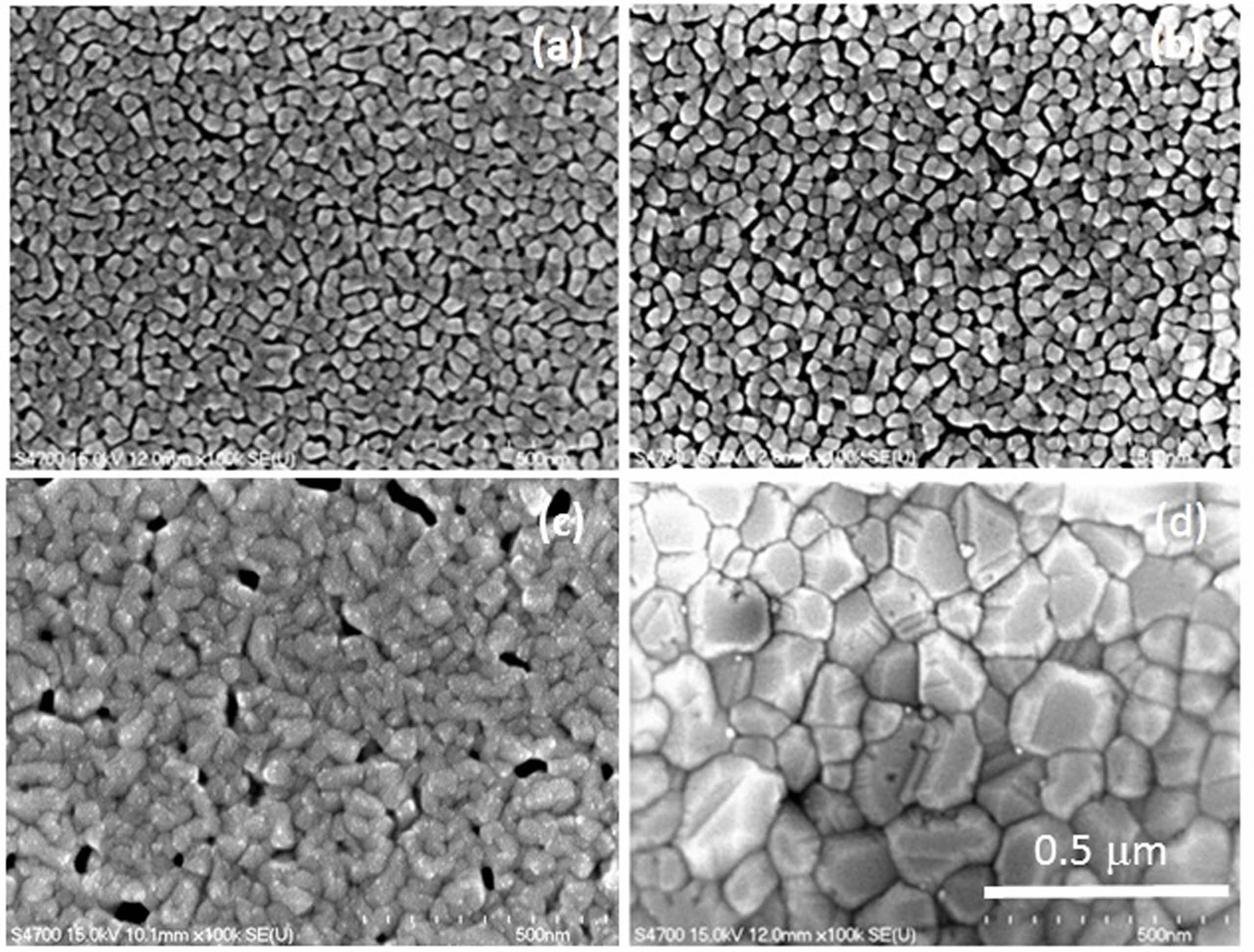
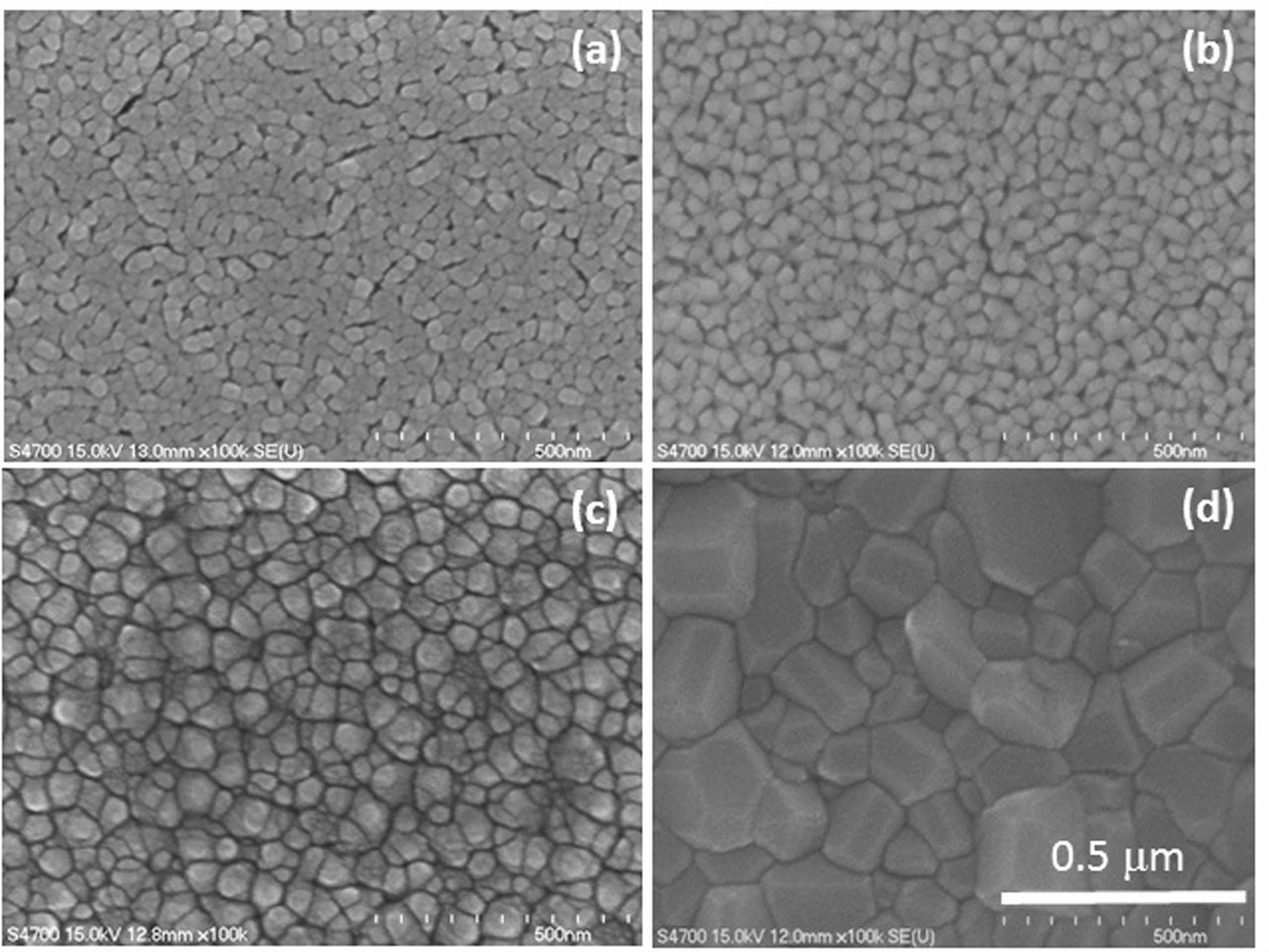
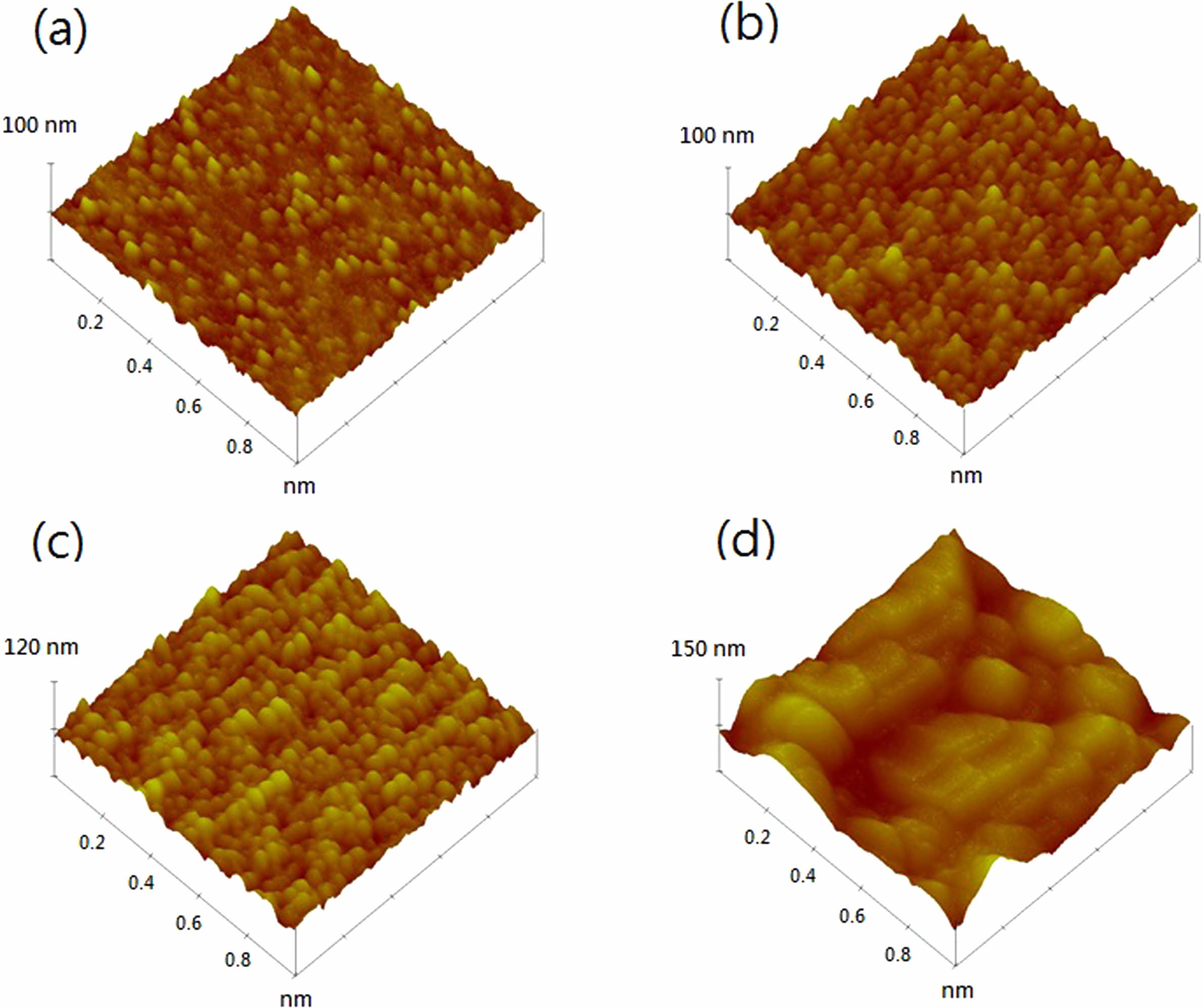
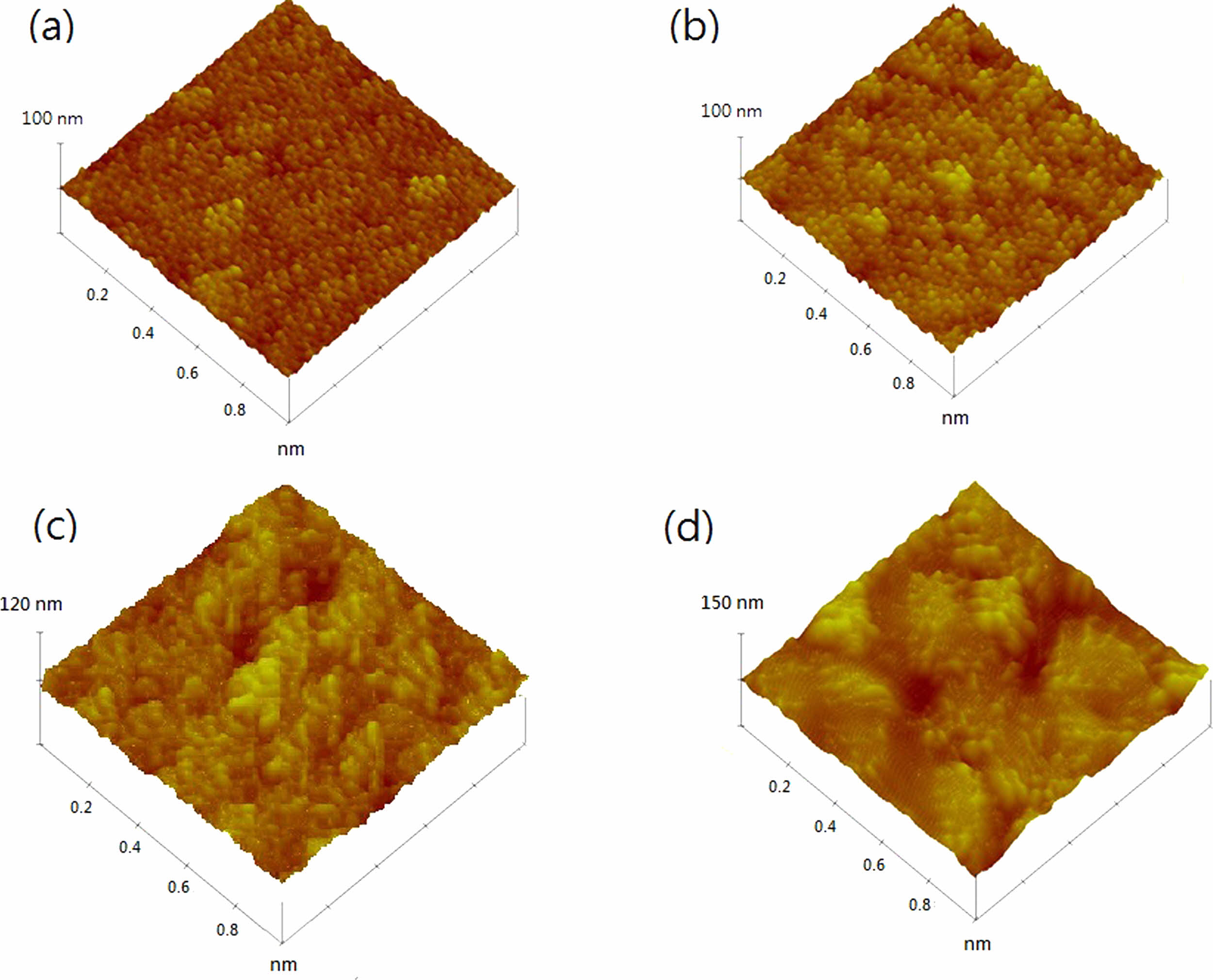
Fig. 1 and 2 shows the FESEM images of the films under Cu concentrations of 0 and 7 wt % annealed at different temperatures. For 7 wt % Cu, all the films exhibited a denser microstructure than those of 0 wt % Cu. In addition, a difference in grain size was also found between these films. The grain size of 0 wt % Cu films has an average grain size of approximately 25-30 nm at room temperature and increased to 90-100 nm at annealing temperature of 550 oC. Where the 7 wt % Cu films showed a larger grain size of approximately 35-40 nm at room temperature and increased to 130-140 nm at annealing temperature of 550 oC. The change in surface morphology of the Cu2O films with 0 and 7 wt % Cu concentrations could be seen in the AFM images shown in Fig. 3 and 4. The Cu2O films prepared without Cu addition were significantly rougher than those of 7 wt % Cu concentration. The root mean square (Rms) roughness of both films is also found to increase with increasing annealing temperature. Rms roughness was approximately 21.2 nm at room temperature and increased up to 63.4 nm as the annealing temperature increased to 550 oC for the film with 0 wt % Cu. For 7 wt % Cu, Rms roughness was approximately 14.8 nm at room temperature and increased to 46.7 nm as the annealing temperature increased to 550 oC. The former with more irregular grains were almost uniform in size and shape, but micropores were seen to spread around the grain boundary and resulted in a rougher film surface.
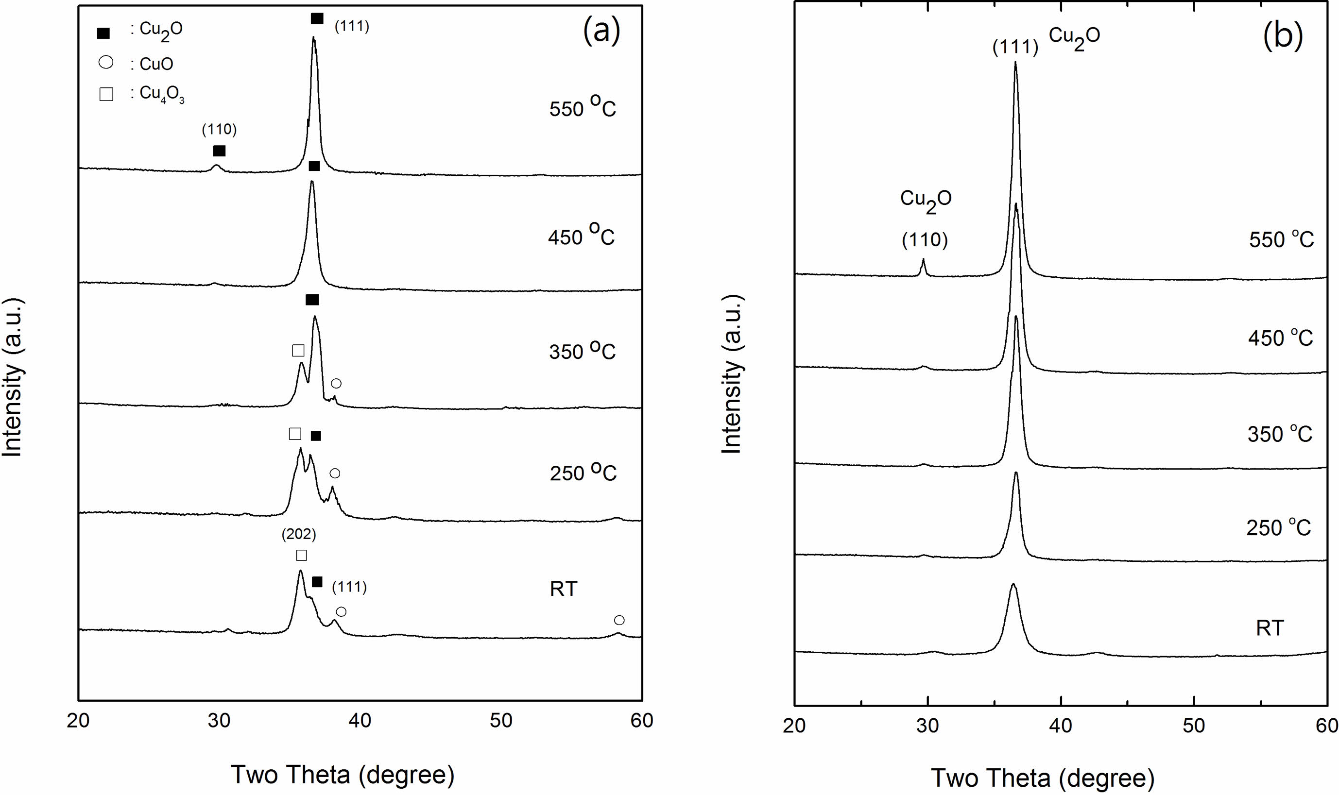
The crystal structure of Cu2O films with Cu concentrations of 0 and 7 wt % prepared on glass substrates was examined by XRD measurements. Fig. 5(a) shows X-ray diffraction patterns of Cu2O films with 0 wt % of Cu concentration. There are three phases of the Cu-O compound can be detected in as-deposited film and the films annealed at temperatures of 250 oC and 350 oC. Cu4O3 phase with the tetragonal structure was the dominant phase at room temperature. The peak can be found at 2θ=35.8 (JCPDS file No. 49-1830) [42]. The other two copper oxide phases were also observed at 2θ=35.4 (JCPDS file No. 48-1548) with respect to the monoclinic phase of CuO and 2θ=36.5 (JCPDS file No. 65-3288) with respect to the cubic phase of Cu2O [43]. Nevertheless, the intensities of the Cu4O3 and CuO phases decreased and finally disappeared at annealing temperature of 450 oC. Further, the intensity of the Cu2O phase increased with the increasing annealing temperature, becoming the only crystalline phase along with the preferred orientation of the (111) reflection peak. For 7 wt % Cu of Cu2O films in Fig. 5(b), only Cu2O phase peaks present at all annealing temperatures, whereas Cu4O3 and CuO phases did not appear in this composition. The (111) peak intensity of Cu2O was also found to increase with increasing annealing temperature, indicating the crystallinity of the Cu2O films is improved.
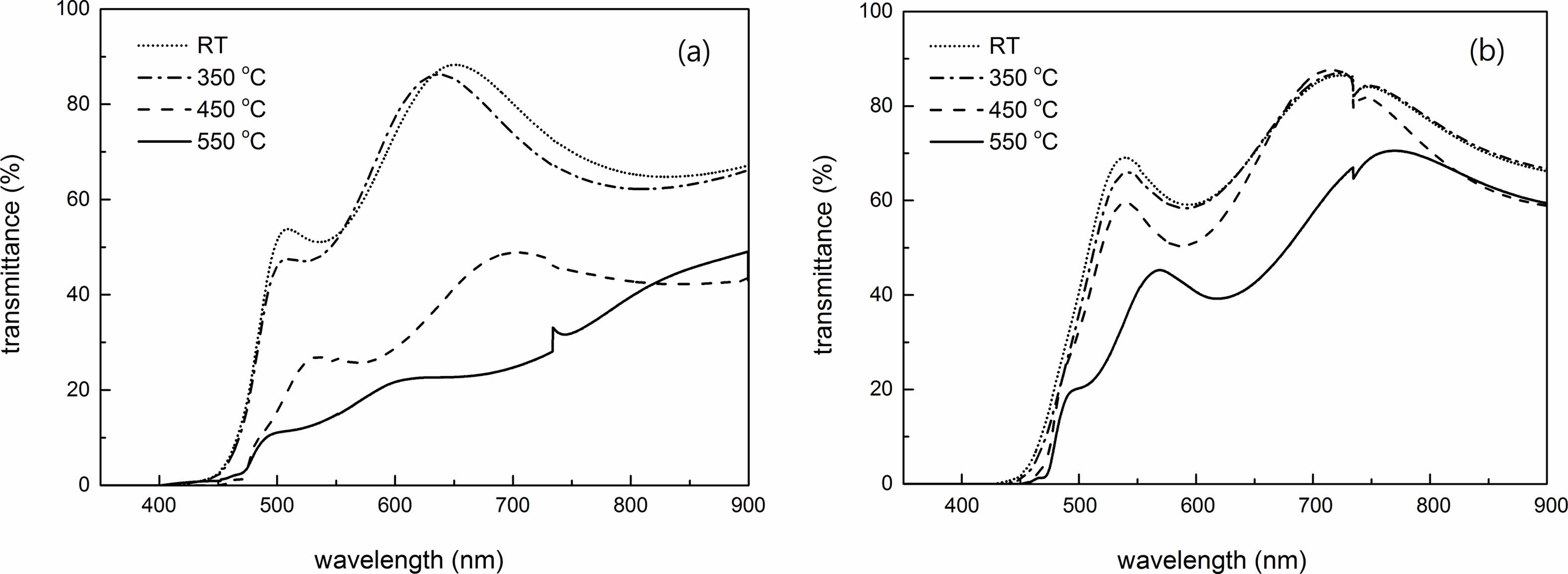
The optical transmittance spectra of 0 and 7 wt % Cu films annealed at different temperatures in visible region are shown in Fig. 6. The transmittance of 7 wt % Cu was greater than that of 0 wt % Cu due to the better crystallinity, larger grain size and lower defect density. However, the transmittance is lower for the samples annealed at higher temperatures. This variation can be related to film structure. As we have seen from AFM data in Fig. 3 and 4, the film surface becomes rough as annealing temperature is increased and resulted in more light scattered and then a low transmittance in the visible region. Drude theory can be used to calculate the optical properties of Cu2O films based on the free carrier absorption of the film [44]. The absorption coefficient, α, of the films therefore was calculated based on the information of transmittance and reflectance from optical spectra, using the following expression:

Where Io is the intensity of incident light, I is the intensity of transmitted light, and d is the thickness of the film. The energy gap, Eg, of the film was then calculated based on the absorption coefficient data from the following relationship,

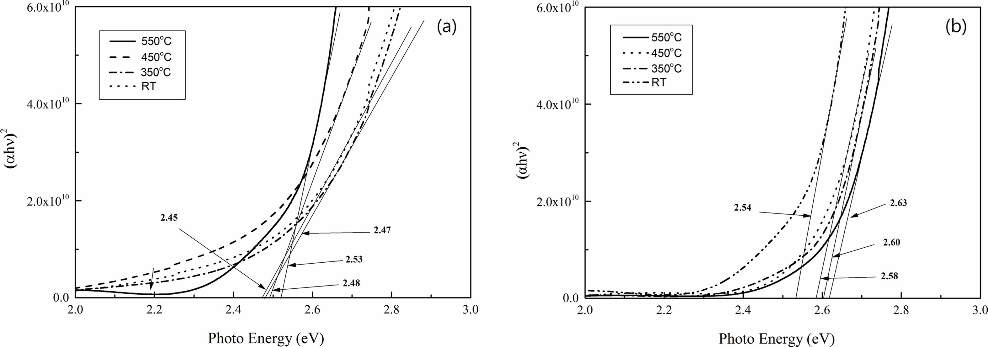
where hv is the photo energy. By plotting α2 as a function of photon energy of the films as shown in Fig. 7, a direct allowed transition was found in these films due to the presence of absorption edge. In addition, the band gaps were also calculated by extrapolating of the linear region to α2 = 0, resulted in the range from 2.54 to 2.63 eV for 7 wt % Cu. These values are little higher than those of 0 wt % Cu, which have Eg values between 2.45 and 2.53 eV. This is possibly because of more free carriers contributed by the samples with 7 wt % Cu concentration.
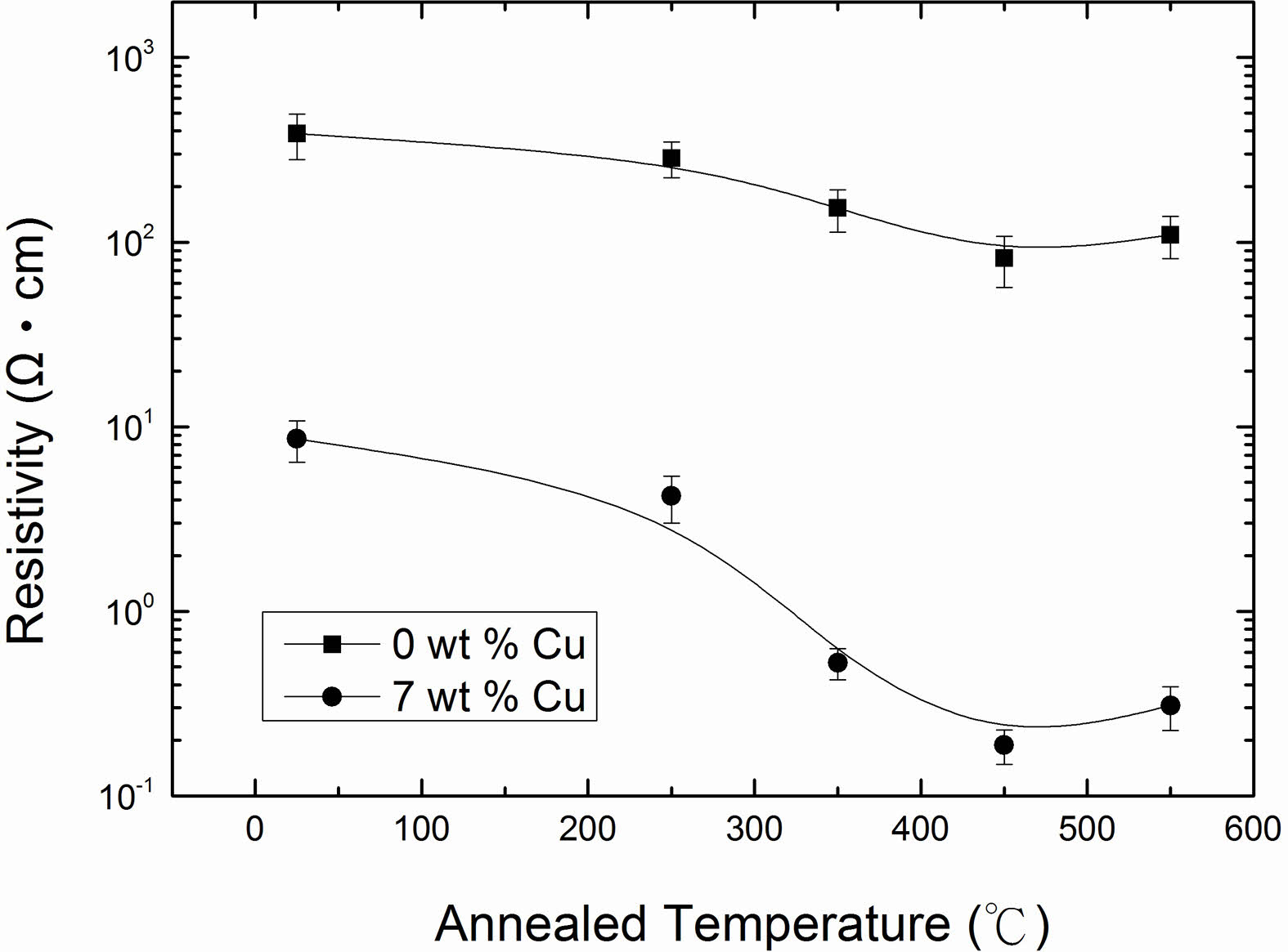
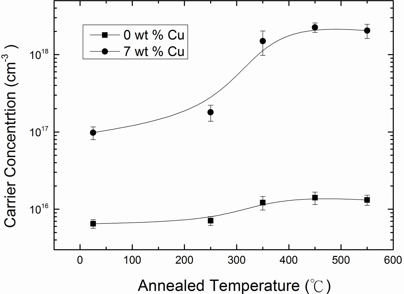
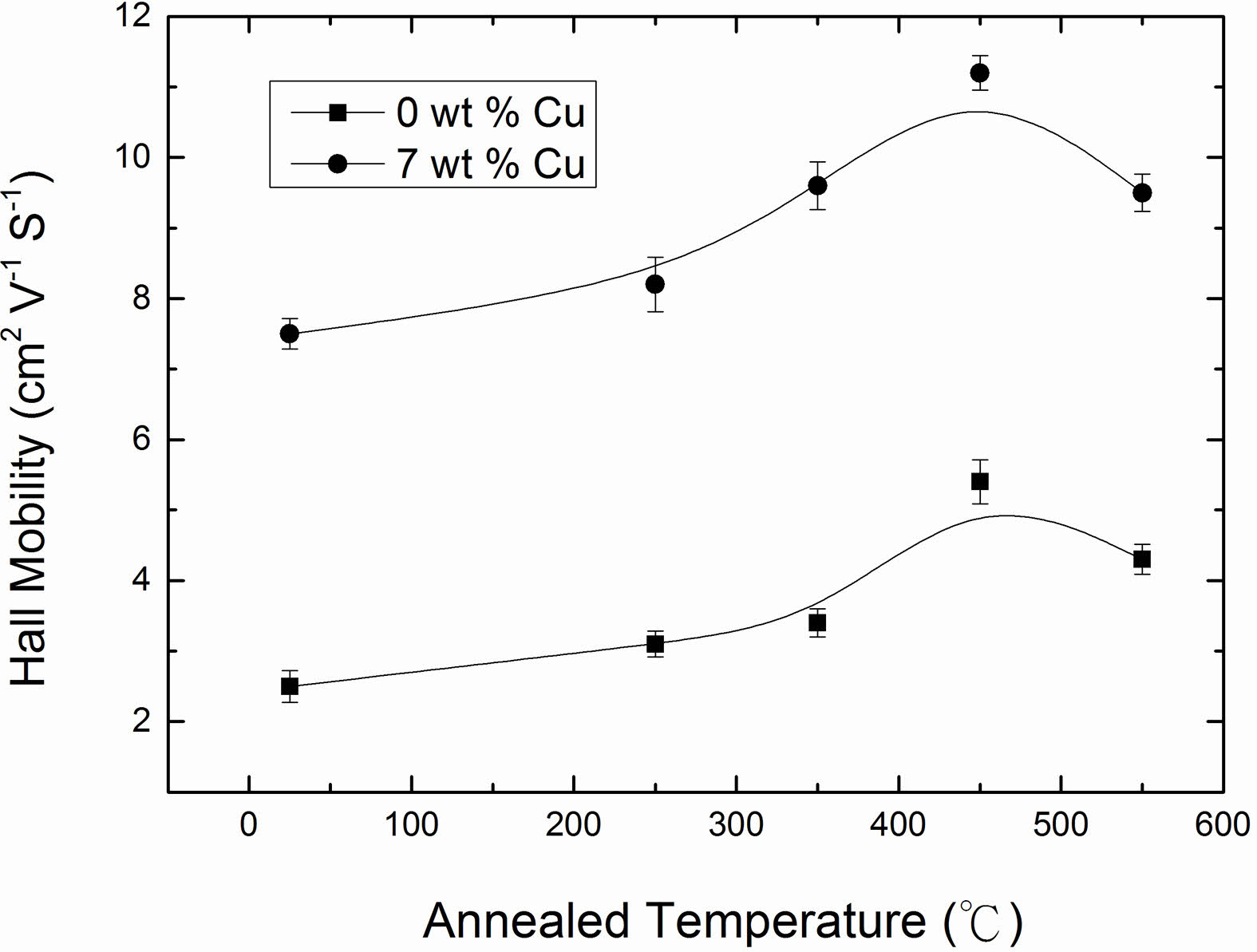
The electrical resistivity of Cu2O films with 0 and 7 wt % Cu concentrations as a function of the annealing temperature, and the results are shown in Fig. 8. The data clearly indicated that the electrical resistivity of the films decreased with increase in annealing temperature and reached to a minimum value at annealing temperature of 450 oC and thereafter increased. The observed decrease in resistivity was correlated to an increase in the carrier concentration and mobility. The carrier concentration and mobility as a function of annealing temperature are plotted in Fig. 9 and 10. It can be seen that as annealing temperature increased from room temperature to 450 oC, both carrier concentration and mobility increased and therefore the resistivity decreased to 109.5 and 0.19 Ω·cm for 0 and 7 wt % of Cu, respectively.
The carrier concentration increased with an increase in annealing temperature due to the improvement of crystallinity of the films. XRD results revealed that the crystallinity of the films was consolidated as annealing temperature increased. However, the carrier concentration of the films reached a saturated value of 1.41 × 1016 cm-3 and 2.25 × 1018 cm-3 for 0 and 7 wt %, respectively at annealed temperature of 450 oC, and began to slightly decrease as seen from Fig. 9. The mechanism of carrier concentration drop in higher annealing temperature can be explained by two causes, one is a reduction of copper vacancies as acceptor and the other is an increase of bivalent Cu as donors [22]. On other hand, the Hall mobility with high degrees of crystallinity was expected to increase with an increase in annealing temperature due to the relatively large grain size and low grain boundary scattering. However, an obvious improvement was not observed at annealing temperature of 550 oC. In addition to grain size, the film surface also has a significant impact on the Hall mobility. From AFM analysis, we have observed larger surface roughness for the films annealed at 550 oC compared to those of films annealed at lower temperatures as mentioned previously. The charge carriers traveling over a rougher surface can be impeded more severely along their mean free path and therefore result in a decrease in mobility [43]. This can explain why the electrical resistivity of the films increased at annealing temperature of 550 oC.
|
Fig. 1 FESEM photo images of 0 wt % Cu annealed at temperatures of (a) room temperature, (b) 350, (c) 450 and (d) 550 oC. |
|
Fig. 2 FESEM photo images of 7 wt % Cu annealed at temperatures of (a) room temperature, (b) 350, (c) 450 and (d) 550 oC |
|
Fig. 3 AFM images of 0 wt % Cu annealed at temperatures of (a) room temperature, (b) 350, (c) 450 and (d) 550 oC. |
|
Fig. 4 AFM images of 7 wt % Cu annealed at temperatures of (a) room temperature, (b) 350, (c) 450 and (d) 550 oC. |
|
Fig. 5 X-ray diffraction patterns of (a) 0 and (b) 7 wt % Cu concentrations of Cu2O film. |
|
Fig. 6 Optical transmittance spectra of Cu2O films at different annealed temperatures for (a) 0 and (b) 7 wt % Cu. |
|
Fig. 7 Optical band gaps as a function of annealed temperatures in Cu2O films for (a) 0 and (b) 7 wt %. |
|
Fig. 8 Electrical resistivity of Cu2O films as a function of annealed temperature for 0 and 7 wt % Cu. |
|
Fig. 9 Carrier concentration of Cu2O films as a function of annealed temperature for 0 and 7 wt % Cu. |
|
Fig. 10 Hall mobility of Cu2O films as a function of annealed temperature for 0 and 7 wt % Cu. |
Transparent and electrical conducting Cu2O films were deposited at room temperature and annealed at 250 to 550 oC using Cu2O/Cu as a composite target with 0 and 7 wt % Cu, respectively. The addition of Cu was found to improve the crystallization and increase the grain size of Cu2O films as well as decreased the surface roughness. In addition, annealing temperature also was found to affect the microstructure, electrical and optical properties of Cu2O films. As annealing temperature increased to 550 oC, grain size of the film increased to 90-100 nm and 130-140 nm for 0 and 7 wt % Cu. However, the surface roughness was also increased to 63.4 and 46.7 nm for both films. As a result, the optimal electrical resistivity of 0.19 Ω·cm was obtained for the films with 7 wt % Cu concentration at annealing temperature of 450 oC, associated with carrier concentration of 2.25 × 1018 cm-3 and mobility of 11.2 cm2·V−1·s−1. The improvement of electrical conductivity was attributed to a better crystallization and larger grain size. Optical transmittance spectra in visible region of Cu2O films were found to decrease with increasing annealing temperature due to the increase of the surface roughness. The band gaps of the Cu2O films were calculated and values are within the range from 2.45 to 2.63 eV.
The authors would like to thank the National Science Council (NSC) of the ROC for the financial support of this study under contract no. NSC-105-2221-E-214-032.
- 1. A.C. Badgujar, B.S. Yadav, G.K. Jha, and S.R. Dhage, Omega 7 (2022) 14203-14210.
-

- 2. B. Tunhoo, S. Kaewkusonwiwat, T. Thiwawong, and K. Onlaor, J. Electron. Mater. 51 (2022) 6903-6912.
-
- 3. M. Ahmed, A. Bakry, E.R. Shaaban, and H. Dalir, J. Mater. Sci.: Mater. Electron. 32 (2021) 11107-11118.
-
- 4. J. Gwamuri, A. Vora, J. Mayandi, D. Güney, P.L. Bergstrom, and J.M. Pearce, Sol. Energy Mater. Sol. Cells 149 (2016) 250-257.
-
- 5. M. Amuthasurabia, J. Chandradassb, V Ramesh Babuc, P.B. Sethupathib, and M.L.J. Martinb, J. Ceram. Process. Res. 8 (2017) 815-818.
-
- 6. K.W. Kim, J. Ceram. Process. Res. 18 (2007) 19-21.
-
- 7. H.A. Al-Jawhari, Mater. Sci. Semicon. Process. 40 (2015) 241.
-
- 8. L. Hu, R.H. Wei, X.W. Tang, W.J. Lu, X.B. Zhu, and Y.P. Sun, J. Appl. Phys. 128 (2020) 140902.
-
- 9. M. Dekkers, G. Rijnders, and D.H.A. Blank, Appl. Phys. Lett. 90 (2007) 021903.
-
- 10. N. Duan, A.W. Sleight, M.K. Jayaraj, and J. Tate, Appl. Phys. Lett. 77 (2000) 1325.
-
- 11. D.O. Scanlon and G.W. Watson, J. Mater. Chem. 21 (2011) 3655-3633.
-
- 12. S.L. Koa, Y. Nohb, C.W. Kima, D. Leea, C. Leed, and C. Jina, J. Ceram. Process. Res. 17 (2016) 213-217.
-
- 13. R. Kisslinger, S. Riddell, S. Savela, P. Kar, U.K. Thakur, S. Zeng, and K. Shankar, J. Mater. Sci.: Mater. Electron. 30 (2019) 11327-11335.
-
- 14. M.L. Liu, L.B. Wu, F.Q. Huang, L.D. Chen, and J.A. Ibers, J. Solid State Chem. 18 (2007) 62-69.
-
- 15. K.H.L. Zhang, K. Xi, M.G. Blamire, and R.G. Egdell, J. Phys.: Condens. Matter. 28 (2016) 383002.
-
- 16. R. Nagarajan, A.D. Draeseke, A.W. Sleight, and J. Tate, J. Appl. Phys. 89 (2001) 8022-8029.
-
- 17. H. Hiramatsu, H. Yanagi, T. Kamiya, K. Ueda, M. Hirano, and H. Hosono, Chem. Mater. 20 (2007) 326-334.
-
- 18. T. Miyata, K. Watanabe, H. Tokunaga, and T. Minamiet, J. Semicon. 40 (2019) 032701.
-
- 19. A. Lakshmanan, Z.C. Alex, and S.R. Meher, Mater. Sci. Semicon. Process. 148 (2022) 106818.
-
- 20. I.S. Han, J.S. Park, and I.K. Park, J. Ceram. Process. Res. 20 (2019) 660-664.
-
- 21. J. Chen, C. Li, J. Zhang, C. Li, J. Chen, and Y. Ren, Materials 11 (2018) 1256.
-
- 22. Y. Nakano, S. Saeki, and T. Morikawa, Appl. Phys. Lett. 94 (2009) 022111.
-
- 23. D. Ozaslana, O.M. Ozkendir, M. Gunes, Y. Ufuktepea, and C. Gumus, Optik 157 (2018) 1325-1330.
-
- 24. A. Sekkat, M.O. Liedke, V.H. Nguyen, M. Butterling, F. Baiutti, J. de D.S. Very, M. Weber, L. Rapenne, D. Bellet, G. Chichgnoud, A. Kaminski-Cachopo, E. Hirschmann, A. Wagner, and D. Munoz-Rojas, Nat. Commun. 13 (2022) 5322.
-
- 25. A. Chen, H. Long, X.C. Li, Y. Li, G. Yang, and P. Lu, Vacuum 83 (2009) 927-930.
-
- 26. M. Guzman, W. Tian, C. Walker, and J.E. Herrera, R. Soc. Open Sci. 9 (2022) 220485.
-
- 27. C. Wadia, A.P. Alivisatos, and D.M. Kammen, Environ. Sci. Technol. 43 (2009) 2072-2077.
-
- 28. H. Kim, M.Y. Lee, S.H. Kim, S.I. Bae, K.Y. Ko, H. Kim, K.W. Kwon, J.H. Hwang, and D.J. Lee, Appl. Surf. Sci. 349 (2015) 673-682.
-
- 29. Y. Aljlan, P. Frank, C.H. On, D.B Robert, F. Lewis, and G. Desmond, Thin Solid Films 642 (2017) 45-50.
-
- 30. Y.G. Lee, J.R. Wang, M.J. Chuang, D.W. Chen, and K.H. Hou, Int. J. Electrochem. Sci. 12 (2017) 507-516.
-
- 31. X. Liu, M. Xu, X. Zhang, and W. Wang, Appl. Surf. Sci. 435 (2018) 305-311.
-
- 32. K. Amikura, T. Kimura, M. Hamada, N. Yokoyama, J. Miyazaki, and Y. Yamada, Appl. Surf. Sci. 254 (2008) 6976-6982.
-
- 33. R.V. Kumar, Y. Mastai, and A. Gedanken, Chem. Mater. 12 (2000) 3892-3895.
-
- 34. J. Medina-Valtierra, C. Frausto-Reyes, G. Camarillo-Martínez, and J.A. Ramírez-Ortiz, Appl. Catal. A 356 (2009) 36-42.
-
- 35. H.J. Li, C.Y Pu, C.Y. Ma, S. Li, W.J. Dong, S.Y. Bao, and Q.Y. Zhang, Thin Solid Films 520 (2011) 212-216.
-
- 36. S.C. Siah, Y.S. Lee, Y. Segal, and T. Buonassisi, J. Appl. Phys. 112 (2012) 084508.
-
- 37. S.H. Lee, S.J. Yen, and J.W. Lim, Electron. Telecom. Res. Inst. J. 35 (2013) 1156-1159.
-
- 38. L.E. Morris, M.I. Ridge, C.A. Bishop, and R.P. Howson, J. Appl. Phys. 51 (1980) 1847-1849.
-
- 39. J.T. Txintxurreta, E.G. Berasategui, R. Ortiz, O. Hernández, L. Mendizábal, and J. Barriga, Coatings 11 (2021) 92-106.
-
- 40. W. Zheng, Y. Chen, X. Peng, K. Zhong, Y. Lin, and Z. Huang, Materials 10 (2018) 1253-1259.
-
- 41. B. Houng, J.K. Wu, P.C. Yeh, W.L. Yeh, and C.K. Sun, J. Electroceram. 45 (2020) 129-134.
-
- 42. N.H. Lam, R.P. Smith, N. Le, C.T.T. Thuy, M.S. Tamboli, A.M. Tamboli, S. Alshehri, M.M. Ghoneim, N.T.N. Truong, and J.H. Jung, Crystals 12 (2022) 566-573.
-
- 43. M.J. Dai, S.S. Lin, Q. Shi, F. Liu, W.X. Wang, S.C. Chen, T.Y. Kuo, and H. Sun, Coatings 10 (2020) 473-482.
-
- 44. H.L. Hartnagel, A.L. Dawar, A.K. Jain, and C. Jagadish, in “Semiconducting transparent thin films” Institute of Physics Publishing, (1995) 141-281.
 This Article
-
2023; 24(5): 788-795
Published on Oct 31, 2023
- 10.36410/jcpr.2023.24.5.788
- Received on May 10, 2023
- Revised on Sep 24, 2023
- Accepted on Sep 29, 2023
Services
- Abstract
introduction
experimental procedure
results and discussion
conclusions
- Acknowledgements
- References
- Full Text PDF
Shared
Correspondence to
- Boen Houng
-
Department of Materials Science and Engineering, I-Shou University, 840 Kaohsiung City, Taiwan
Tel : 011-886-76579708 Fax: 011-886-76578444 - E-mail: boyen@ isu.edu.tw
Clean-Energy Research Institute(CRI), Hanyang University, 222, Wangsimni-ro, Seongdong-gu, Seoul, 04763, Korea
E-mail: jcpr@hanyang.ac.kr