


- Structural and electrical properties of La-Sr-Mn-O ceramics with Bi3+ content for thermistor devices
Do-Hui Kima, Jeong-Eun Limb, Byeong-Jun Parkb, Sam-Haeng Yib,c, Myung-Gyu Leeb,c, Joo-Seok Parkc and Sung-Gap Leea,b,*
aMajor in Ceramic Engineering, School of Materials Science and Engineering, Gyeongsang National University, Jinju 52828, Korea
bDepartment of Materials Engineering and Convergence Technology, Research Institute for Green Convergence Technology, Gyeongsang National University, Jinju 52828, Korea
cBusiness Support Division, Korea Institute of Ceramic Engineering and Technology, Jinju 52851, KoreaThis article is an open access article distributed under the terms of the Creative Commons Attribution Non-Commercial License (http://creativecommons.org/licenses/by-nc/4.0) which permits unrestricted non-commercial use, distribution, and reproduction in any medium, provided the original work is properly cited.
La0.7Sr0.3-xBixMnO3 (LSBMO) (0.025 ≤ x ≤ 0.15) films are fabricated by a sol-gel method and spin-coating method. All of the fabricated films have typical polycrystalline perovskite structures. In addition, no preferential orientation or impurity could be observed. The surface SEM images show almost homogeneous and uniform microstructures and the average thickness for the LSBMO films is approximately 230 to 260 nm. When the resistivity is measured at room temperature, the TCR and B85/25-values gradually increases as the amount of Bi3+ increased, and the highest values of 0.023 mΩ·cm, 0.31%/°C and 299 K are obtained in the La0.7Sr0.225Bi0.075MnO3 thin films. Polycrystalline LSBMO films follow the variable-range hopping (VRH) conduction model as they show electron-electron scattering and electron-phonon interactions for thermal stimulation
Keywords: La0.7Sr0.3-xBixMnO3 films, Sol-gel method, Structural properties, Electrical properties, Thermistor
Perovskite-structured manganese-based R1-xAxMnO3 (R=trivalent rare-earth, A=divalent alkaline-earth ions) compounds exhibit colossal magnetoresistance (CMR) caused by the transition between a low-temperature ferromagnetic metallic and a high-temperature paramagnetic insulation state depending on constituent elements, applied temperature and magnetic fields [1]. These properties result from Mn3+ with 3d4 (t32g, e1g) electronic arrays converting to Mn4+ with 3d3 (t32g, e0g) electron arrays to maintain electrical neutrality because A2+ ions are generally substituted at R3+ sites. High electrical conduction is exhibited by the double exchange (DE) of electrons with strong on-site Hund’s coupling between the partially filled d-shell of Mn3+ and Mn4+ in the perovskite MnO6 oxygen octahedral structure [2]. These CMR characteristics have given rise to a variety of studies focused on new functional oxide material devices, such as magnetic information storage devices, sensors and spintronics devices [3, 4]. One of the best conductive oxide materials is La1-xSrxMnO3, which has an electrical conductivity that is greatly affected by the Jahn-Teller distortion of the unit lattice due to a difference in the ion radius of Mn4+/Mn3+, and La3+ (0.136 nm) and Sr2+ (0.144 nm) according to the composition ratio of Sr2+ [5, 6]. Furthermore, the electrical conduction characteristics depend heavily on microstructural characteristics such as the grain of the grains, grain boundaries, pores and oxygen attackers in accordance with the manufacturing of bulk or thin films [7].
La0.7Sr0.3MnO3 (LSMO) exhibited the excellent electrical conductivity and CMR properties at room temperature due to its semi-metallic ferromagnetic characteristics [8]. In this study, we fabricated La0.7Sr0.3-xBixMnO3 by substituting a portion of Sr2+ ions with Bi3+ ions, which have different atomic and ionic radii, using the sol-gel method. We then observed the structural and electrical properties as a function of composition ratio to investigate the possibility of application as a thermistor devices or bolometer-type infrared detectors operating at room temperature.
Manganese acetate (Mn(CH3COO)2·4H2), lanthanum acetate (La(CH3COO)3·xH2O), strontium acetate (Sr(CH3COO)2) and bismuth acetate (Bi(CH3COO)3) were dissolved into acetic acid, ethyl alcohol and distilled water co-solvents to drive the La0.7Sr0.3-xBixMnO3 (0.025 ≤ x ≤ 0.15) (LSBMO) precursor solutions. The precursor solutions were aged for 24 hours before deposition. LSBMO coating solutions were spin-coated on cleaned Pt/Ti/SiO2/Si substrates at 4,000 rpm for 30 seconds. The coated thin films were dried and annealed at 200 °C for 5 min. and at 400 °C for 10 min., respectively. The spin-coating, drying and pyrolysis cycle was repeated six times. Finally, the films were crystallized at 800 oC for 60 min. in an oxygen atmosphere. The crystallographic and structural properties of the films were measured using X-ray diffraction (XRD), field-emission scanning electron microscopy (FE-SEM), and X-ray photoelectron spectroscopy (XPS), and the electrical properties were measured by the Van der Pauw method using an electrometer (Keithley 6517A, USA).
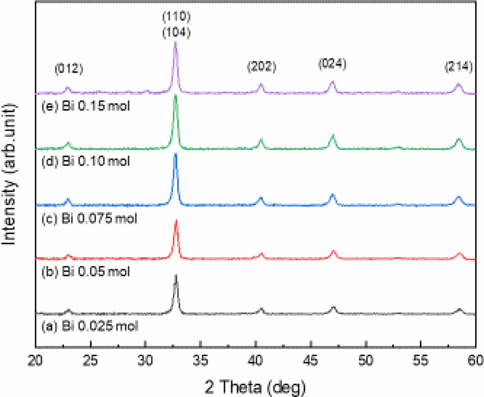
Fig. 1 shows the X-ray diffraction patterns according to the amount of Bi3+ in the LSBMO films. All of the films have a typical perovskite structure with no preferential orientations or impurities Perovskite LaMnO3 adopts an orthorhombic structure at room temperature, and shows a rhombohedral structure by distortion of the ABO3 unit cell as Sr2+ ions with a larger ionic radius is added to the A-site La3+ ions [9]. LSMO has a polycrystalline perovskite crystal structure with a rhombohedral crystal structure in which an X-ray diffraction peak is separated near the diffraction angle of 2θ=33o [10]. However, LSBMO showed an orthorhombic crystal structure with a single peak, which is believed to be due to decrease of the distortion of the unit lattice caused by the addition of the smaller ionic radius Bi3+ (0.117 nm) [11].
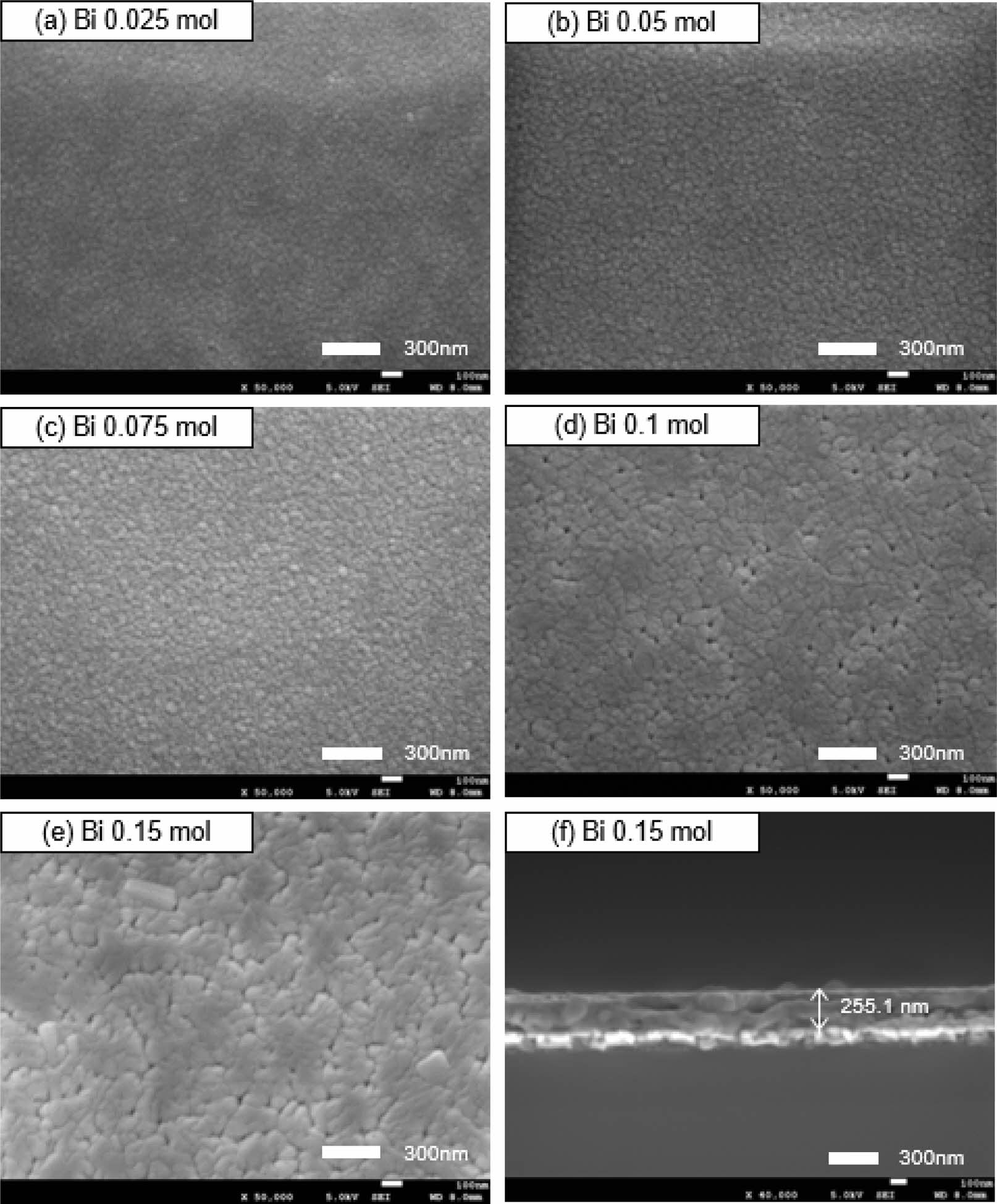
Fig. 2 shows the surface (a~e) and cross-sectional (f) microstructures of the LSBMO films according to the amount of Bi3+. The surface SEM images show almost homogeneous and uniform microstructures. The average grain size tended to increase as the amount of Bi3+ increased, and some small surface pores were observed in the La0.7Sr0.15Bi0.15MnO3 film. This is believed to be due to the volatilization of Bi (m.p.=825 oC), which has a low melting point, or surface irregularities due to the growth of grains in the vertical direction of the substrate [12]. The amount of Bi3+ did not seem to influence the thickness of the LSBMO films, and the average thickness for all films was approximately 230 to 260 nm.
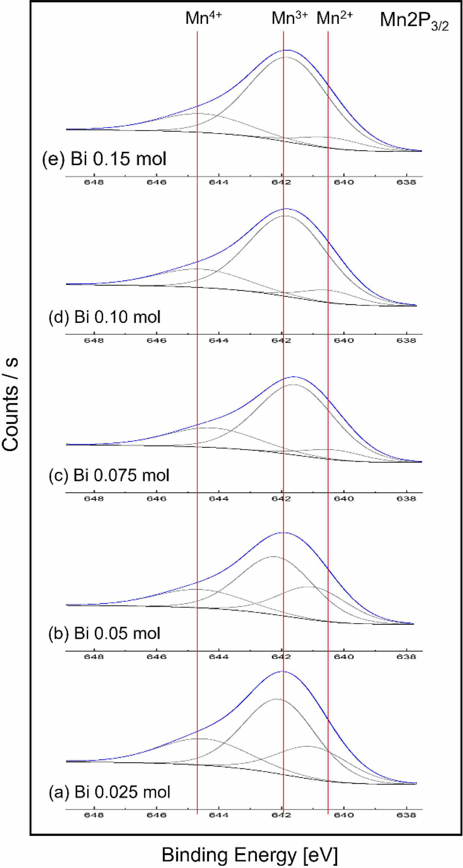
Fig. 3 shows the XPS analysis results of the Mn 2p3/2 orbit according to the Bi3+ amount in the LSBMO films. The binding energies of Mn2+, Mn3+ and Mn4+ ions were not observed as dependent on the amount of Bi3+, and were approximately 640.3 to 641.0 eV, 641.5 to 642.16 eV and 644.23 to 644.6 eV, respectively. However, as the Bi3+ amount increased, the Mn4+/Mn3+ ratio tended to decrease, which is believed to be because the generation of Mn4+ formed to maintain the electrical neutrality of the unit lattice was suppressed by Bi3+ addition [13]. The shape of the Mn 2p signal of the LSBMO films implies that the majority of the Mn ions are in the Mn3+ state.
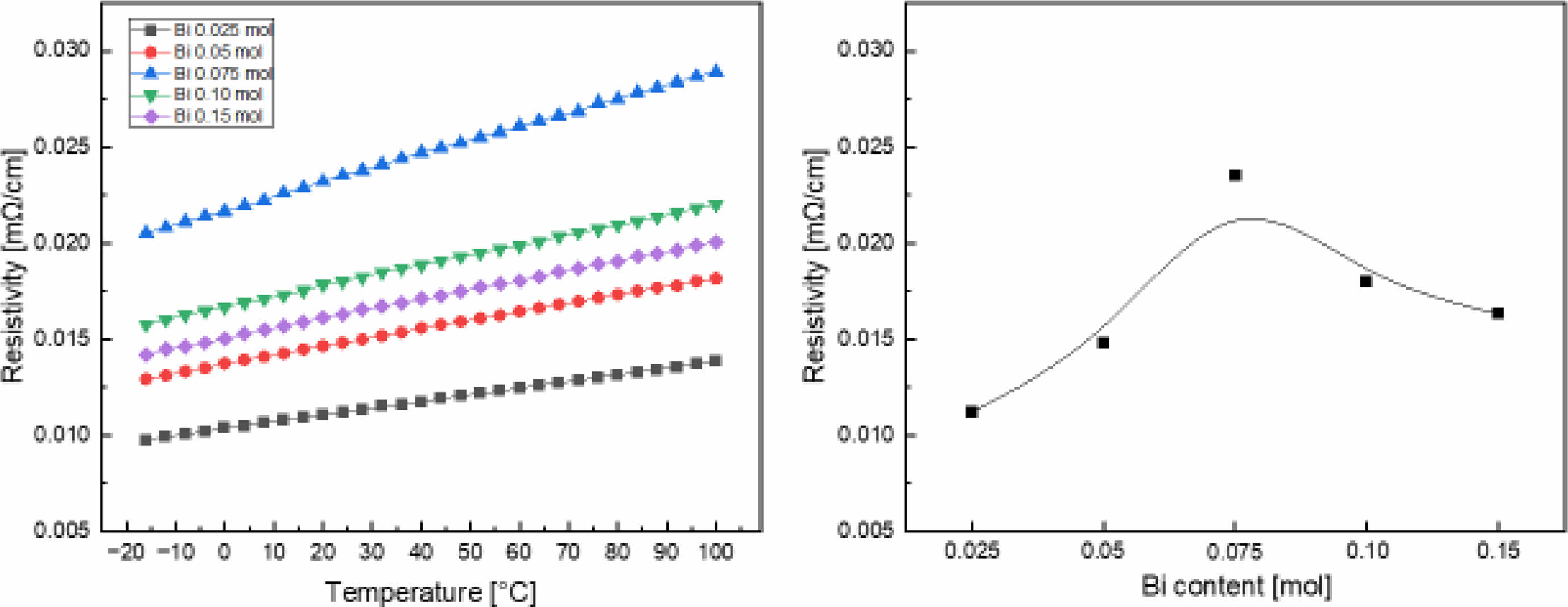
Fig. 4 shows the resistivity of the LSBMO films according to the amount of Bi3+ and temperature. All films showed typical ferromagnetic metallic properties in which resistivity increases as temperature increases [14]. The resistivity at room temperature increased as the amount of Bi3+ increased, and decreased after reaching a maximum value of 0.023 mΩ·cm at 0.075 mol. In general, the electrical conduction properties of LSMO result from the DE interaction of the outermost electrons of Mn3+ and Mn4+ via oxygen ions in a perovskite lattice, and the electrical conduction properties are affected by the Mn-O bond distance and the Mn-O-Mn bond angle [15]. As shown in the XPS in Fig. 3, as the amount of Bi3+ increased, the resistivity increased because of the decrease in the Mn4+/Mn3+ ratio. However, when 0.10 mol or more Bi3+ is added, the Mn-O binding distance is decreased by the addition of Bi3+ (0.114 nm), which has a small ion radius, the hopping probability is increased and the resistivity is decreased. Further research is needed on the relationship between the transfer interaction of the eg conduction electrons and the Jahn-Teller distortion caused by impurities with different valences and ionic radii to better understand the electrical conduction mechanism of LSMO materials.
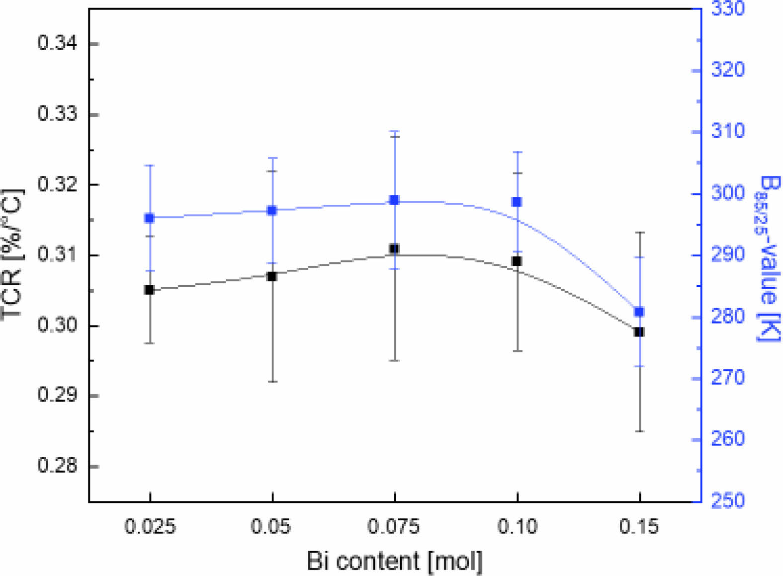
Fig. 5 shows the temperature coefficient of resistance (TCRd, TCR = (1/RT)(dRT/dT); RT is resistance measured at T (oC)) and the B85/25-value (B35/25 = (lnR1 - lnR2)/(1/T1 - 1/T2), where R1 and R2 are the resistance measured at T1 (25 oC) and T2 (85 oC), respectively) according to the amount of Bi3+ in the LSBMO films. The TCR and B85/25-value gradually increased as the amount of Bi3+ increased, and were the highest at 0.31%/oC and 299 K with 0.075 mol Bi3+, respectively. When 0.10 mol or more Bi3+ was added, the TCR and B85/25-value tended to decrease. The crystal structure of perovskite R1-xAxMnO3 is affected by the lattice distortion caused by the ionic radius of the cation located at the A-site, and its structural stability is expressed by the tolerance factor (t). An ideal cubic crystal structure without internal compressive or tensile strain is represented by t = 1, a rhombohedral structure is represented by 0.96 < t < 1 and an orthorhombic structure is represented by t < 0.96 [16]. The La0.7Sr0.225Bi0.075MnO3 film has a t of 0.9618, and is considered to have increased resistance change sensitivity due to thermal stimulation increases caused by the mixing of the rhombohedral and orthorhombic phases, resulting in an excellent TCR and B-value.
When the amount of Bi3+ added was 0.10 mol or more, the electrical conduction properties decreased due to the scattering effect of carriers in the pores and grain boundaries, as observed in Fig. 2 [17].
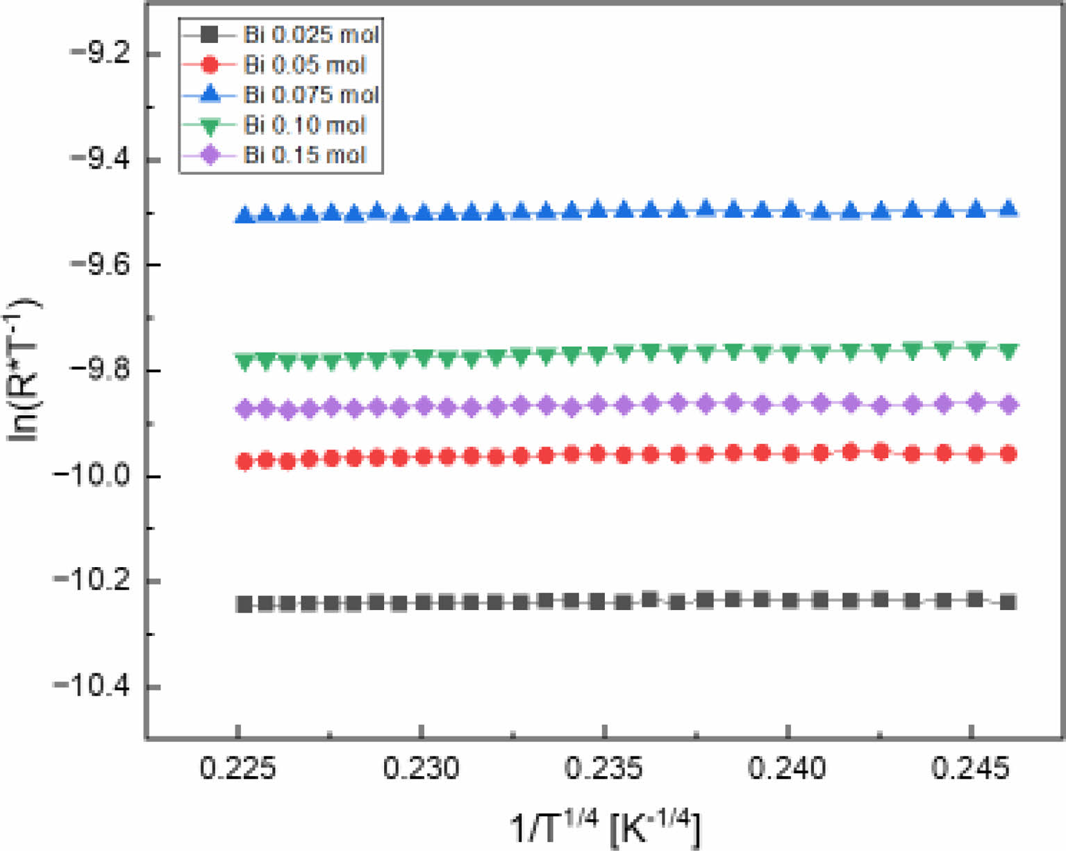
The electrical conduction of LSMO materials depends on the Mn4+/Mn3+ ratio and the Mn-O-Mn hopping probability. Polaron hopping transport according to temperature changes is generally expressed as follows [18]: R = CoTa exp(To/T)p, where R is the resistance, Co is the constant, T is the temperature, and To is the characteristic temperature. α = p = 1 is the nearest-neighbor hopping (NNH) model, and α = 4p is the variable-range hopping (VRH) model. The VRH model describes the jump of charge carriers from a localized state to another state [13]. Fig. 6 shows the ln(R·T -1) vs 1/T 1/4 curve of the LSBMO films according to the amount of Bi3+, and shows good linearity in all films. This is thought to be due to electron-electron scattering and electron-phone interactions caused by thermal stimulation in the polycrystalline thin films in which crystal grains, grain boundaries and point defects are distributed [19, 20].
|
Fig. 1 X-ray diffraction patterns of LSBMO films with variation of Bi3+ contents. |
|
Fig. 2 (a)~(e) surface and (f) cross-sectional SEM micrographs of LSBMO films with variation of Bi3+ contents. |
|
Fig. 3 XPS narrow scans of Mn 2P3/2 of LSBMO films with variation of Bi3+ contents. |
|
Fig. 4 Resistivity of LSBMO films with variation of Bi3+ contents. |
|
Fig. 5 TCR and B85/25-value of LSBMO films with variation of Bi3+ contents. |
|
Fig. 6 ln(R·T-1) vs 1/T1/4 curves of LSBMO films with variation of Bi3+ contents. |
La0.7Sr0.3-xBixMnO3 (0.025 ≤ x ≤ 0.15) films showed the typical polycrystalline perovskite XRD patterns without any observable preferential orientations or impurities. The Mn4+/Mn3+ ratio tended to decrease as the amount of Bi3+ added increased. The shape of the Mn 2p orbital XPS signal of LSBMO films indicated that the majority of the Mn ions were in the Mn3+ state. The LSBMO films showed ferromagnetic metallic characteristics, and the electrical resistance properties are considered to be mutually affected by the transfer interaction of the eg conduction electrons and Jahn-Teller distortion of the unit lattice. The electrical conduction mechanism of the LSBMO films showed VRH model dependence due to electron-electron scattering and electron-phone interactions via thermal stimulation in the polycrystalline films in which crystal grains, grain boundaries, and point defects are distributed. La0.7Sr0.225Bi0.075MnO3 film exhibited a good TCR and B85/25-value, and is expected to be applicable for thermistor devices.
This research was supported by Basic Science Research Program through the National Research Foundation of Korea (NRF) funded by the Ministry of Education (2020R1A6A1A03038697). This work was supported by the National Research Foundation of Korea (NRF) grant funded by the Korea government (MSIT) (2021R1I1A3052426), and the Technology Innovation Program (20020478) funded By the Ministry of Trade, Industry & Energy (MOTIE, Korea).
- 1. C. Sen, G. Alvarez, and E. Dagotto, Phys. Rev. Lett. 98 (2007) 127202.
-

- 2. J. Hemberger, A. Krimmel, T. Kurz, H. von Nidda, V. Inanov, A. Mukhin, A. Balbashov, and A. Loidl, Phys. Rev. B 66 (2002) 094410.
-
- 3. H. Heremans, J. Phys. D: Appl. Phys. 26[8] (1993) 1149-1168.
-
- 4. L. Mechin, J.M. Routoure, B. Guillet, F. Yang, S. Flament, D. Robbes, and R.A. Chakalov, Appl. Phys. Lett. 87 (2005) 204103.
-
- 5. A. Urushibara, Y. Moritomo, T. Arima, A. Asamitsu, G. Kido, and Y. Tokura, Phys. Rev. B 51[20] (1995) 14103-14109.
-
- 6. L.M. Rodriguez-Martinez and J.P. Attfield, Phys. Rev. B 58[5] (1998) 2426-2429.
-
- 7. X. Liu, Z. Jiao, K. Nakamura, T. Hatano, and Y. Zeng, J. Appl. Phys. 87[5] (2000) 2431-2436.
-
- 8. S. Kumari, N. Mottaghi, C.Y. Huang, R. Trappen, G. Bhandari, S. Yousefi, G. Cabrera, M.S. Seehra, and M.B. Holcomb, Sci. Rep. 10 (2020) 3659.
-
- 9. P. Norby, I.G. Anderson, E. Anderson, and N. Anderson, J. Solid State Chem. 119[1] (1995) 191-196.
-
- 10. A. Elghoul, A. Krichene, N.C. Boudjada, and W. Boujelben, Ceramics International 44[11] (2018) 12723- 12730.
-
- 11. N. Nedelko, S. Lewinska, A. Pashchenko, I. Radelytskyi, R. Diduszko, E. Zubov, W. Lisowski, J.W. Sobczak, K. Dyakonov, A. S´lawska-Waniewska, V. Dyakonov, and H. Szymczak, J. Alloys Compd. 640 (2015) 433-439.
-
- 12. S. Wu, X. Wei, X. Wang, H. Yang, and S. Gao, J. Mater. Technol. 26[5] (2010) 472-476.
-
- 13. H. Xie, H. Huang, N. Cao, C. Zhou, D. Niu, and Y. Gao, Phys. B: Cond. Matt. 477[15] (2015) 14-19.
-
- 14. A. Elghoul, A. Krichene, and W. Boujelben, J. Phys. Chem. Solid 98 (2016) 263-270.
-
- 15. L.M. Rodriguez-Martinez and J.P. Attfield, Phys. Rev. B 54[22] (1996) 622- 625.
-
- 16. J.P. Zhou, J.T. McDevitt, J.S. Zhou, H.Q. Yin, J.B. Goodenough, Y. Gim, and Q.X. Jia, Appl. Phys. Lett. 75[8] (1999) 1146-1148.
-
- 17. X. Yu, S. Jin, H. Li, X. Guan, X. Gu, and X. Liu, Appl. Surf. Sci. 570 (2021) 151221.
-
- 18. N. Mott, Conduction in Non-Crystalline Materials, Clarendon, Oxford, 1993.
- 19. D.C. Worledge, G. Jeffrey Snyder, M.R. Beasley, T.H. Geballe, Ron Hiskes, Steve DiCarolis, J. Appl. Phys. 80[9] (1996) 5158-5161.
-
- 20. M. Viret, L. Ranno, and J.M.D. Coey, Phys. Rev. B 55[13] (1997) 8067-8070.
-
 This Article
-
2023; 24(4): 650-654
Published on Aug 31, 2023
- 10.36410/jcpr.2023.24.4.650
- Received on Apr 12, 2023
- Revised on Jul 10, 2023
- Accepted on Jul 14, 2023
Services
- Abstract
introduction
experimental
results and discussion
conclusion
- Acknowledgements
- References
- Full Text PDF
Shared
Correspondence to
- Sung-Gap Lee
-
aMajor in Ceramic Engineering, School of Materials Science and Engineering, Gyeongsang National University, Jinju 52828, Korea
bDepartment of Materials Engineering and Convergence Technology, Research Institute for Green Convergence Technology, Gyeongsang National University, Jinju 52828, Korea
Tel : +82-10-2686-4427 Fax: +82-55-772-1689 - E-mail: lsgap@gnu.ac.kr
Clean-Energy Research Institute(CRI), Hanyang University, 222, Wangsimni-ro, Seongdong-gu, Seoul, 04763, Korea
E-mail: jcpr@hanyang.ac.kr