


- Low-temperature dielectric and impedance properties of SrSn0.2Ti0.8O3 ceramics
Depeng Wang, Ruifeng Niu, Liqi Cui and Weitian Wang*
School of Physics and Electronic Information, Yantai University, Yantai 264005, P.R. China
This article is an open access article distributed under the terms of the Creative Commons Attribution Non-Commercial License (http://creativecommons.org/licenses/by-nc/4.0) which permits unrestricted non-commercial use, distribution, and reproduction in any medium, provided the original work is properly cited.
Tin-doped and undoped perovskite SrTiO3 ceramics were synthesized by solid-state reaction method using SrCO3, TiO2 and SnO2 powders as raw materials. When the samples sintered at 1400 ℃, the SrSn0.2Ti0.8O3 and SrTiO3 ceramics all crystallized in cubic structures. The lattice parameters of SrSn0.2Ti0.8O3 are slightly larger than that of SrTiO3 due to the bigger size of Sn4+ ions. The frequency-dependent dielectric and impedance properties of SrSn0.2Ti0.8O3 ceramics were investigated in the temperature range of 300-100 K. The obtained value of low-temperature dielectric permittivity is larger than 10000, and that of dielectric loss is lower than 0.018 at f = 1 kHz. The impedance spectra were used to show the grains and grain boundaries effects in SrSn0.2Ti0.8O3 ceramics. The calculated electrical conductivity demonstrates the semiconductor properties of the prepared samples. The results indicate that SrSn0.2Ti0.8O3 ceramics have potential applications in dielectric and electronic devices
Keywords: Ceramics, Dielectric properties, Impedance analysis
It is well known nowadays that all kinds of electrical devices are pursuing higher energy storage and less electronic components. In the past decade, oxide ceramics with high dielectric constant and low loss have developed rapidly [1]. Strontium titanate (SrTiO3, STO) adopts cubic perovskite-type structure with space group {{{EQUATIONS}}} and Sr2+ and Ti4+ occupy a quarter of the octahedral interstices. The Curie temperature of STO is -250 ℃ and the STO takes in a paramedical phase at room temperature [2]. Because of its excellent properties such as high dielectric constant, low dielectric loss and relatively high dielectric breakdown strength (~200 kV/cm), STO ceramics are widely used in the field of thermistors, capacitors, access memory and photocatalysts [3, 4].
Generally, the research of STO-based ceramics mainly focuses on reducing the dielectric loss and improving the dielectric constant to adapt to different application situations. Many attempts have been made to improve the energy storage performance. Doping with different metal ions such as Ba2+, Fe3+, and trivalent rare earth is considered to be an effective way to improve dielectric properties. It has been reported that Zr-doped and Y2O3-doped STO materials exhibit interesting electrical and thermoelectrical properties, the doping effects on random porosity, grains and grain boundary are believed to be the main reason for the improved electrical and dielectric performance [5, 6]. In practice, there are two kinds of doped ions which can be introduced into Sr-site or Ti-site in the substitutional mode, including donor ions and acceptor ions. The Sr2+ or Ti4+ ions in STO can be replaced by metal ions with high valence state, resulting in the generation of hole carriers. Similarly, the electron carriers will be generated when Sr2+ or Ti4+ ions are substituted by low-valence metal ions [7]. Moreover, doping ions with different valence states and sizes can generate lattice defects and oxygen vacancies in the oxide materials [8], which contribute to the increase of dielectric permittivity according to the electron pinning defect-dipole effects. However, in terms of the relationship between dielectric constant and breakdown strength, increasing the dielectric constant comes at the cost of increasing the breakdown strength. By considering various factors, choosing appropriate doping ions is important for the improvement of dielectric properties of STO ceramics. Recently, stannates have attracted considerable attentions because of their interesting electrical and capacitive properties. The size of Sn4+ is 0.69 Å, which is similar to that of Ti4+ (0.61 Å). Tin-doped STO ceramics (SrSn0.2Ti0.8O3, SSTO) are perovskite materials with special electrical, magnetic and optical properties, and therefore have applications in many fields, such as sensors, optical devices, thermoelectric materials and superconducting materials. The application of SSTO in the field of high-temperature superconductivity lies in the fact that it can be used as an ideal substrate for high-frequency superconducting materials, such as for the preparation of iron-based superconductor [9, 10]. However, the effect of Sn doping on the dielectric properties of STO ceramics is less studied. In this paper, SrSn0.2Ti0.8O3 (SSTO) ceramics were prepared by using solid-state reaction method and the structure, low-temperature dielectric and conductivity properties of SSTO ceramics were investigated.
Poly-crystalline SSTO samples were prepared by thermal annealing process through traditional solid state reaction. The precursors of high-purity (≥ 99.5%) powders (SrCO3, TiO2, SnO2) with appropriate element molar ratio were weighed by using an analytical balance, and the raw materials were fully mixed to produce a uniform mixture, which was placed in an alumina crucible and pre-sintered in a Muffle furnace at 1300 ℃ for 3 h. Then the powder was ground with an agate mortar for 4 h and dried at 200 ℃ for 2 h. The treated powder was placed in a cylindrical matrix and pressed uniaxial at a pressure of 10 Mpa to obtain high-density pellets with a diameter of 10 mm and a thickness of 1 mm, which were sintered in Muffle furnace at 1400 ℃ for 4 h to fabricate SSTO ceramics. Structural phases were analyzed by using x-ray diffraction (XRD) with a Cu Kα source at 1.54 Ǻ. Low-temperature dependence of complex dielectric properties were measured on a QuadTech 1730 LCR Digibridge over a frequency range of 100 Hz-1 MHz. The impedance spectroscopy was examined by using a HP4194A analyzer with signal amplitude of 50 mV. Data were taken in a temperature range of 300-100 K.
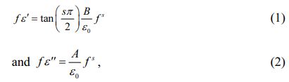
Figure 1(a) shows the XRD pattern of the fabricated SSTO ceramics. A profile of undoped STO prepared under the same conditions is displayed at the bottom of Fig. 1(a) for comparison. The location of all the diffraction peaks of SSTO could be indexed to a cubic phase with the space group Pm3m, and no impurity could be detected indicating that the fabricated SSTO crystallize in a single phase. Compared with the peaks of STO, it is found that doping of Sn4+ with 20 at% concentration do not change the structure of STO seriously. However, the locations of SSTO diffraction peaks shift to lower degree with the doping of Sn4+. This trend of (110) peak is manifested in Fig. 1(b), and the shift value is about 0.17° as marked in the figure. The calculated lattice constant of SSTO is about 3.927 Å, which is about 0.56% larger than that of STO (3.905 Å). The inset of Fig. 1(b) shows the schematic illustration of SSTO crystal structure. As is known, the size of Sn4+ is larger than that of Ti4+. Doping with larger ions will lead to the increased lattice constant, which is responsible for the shift of diffraction peaks.
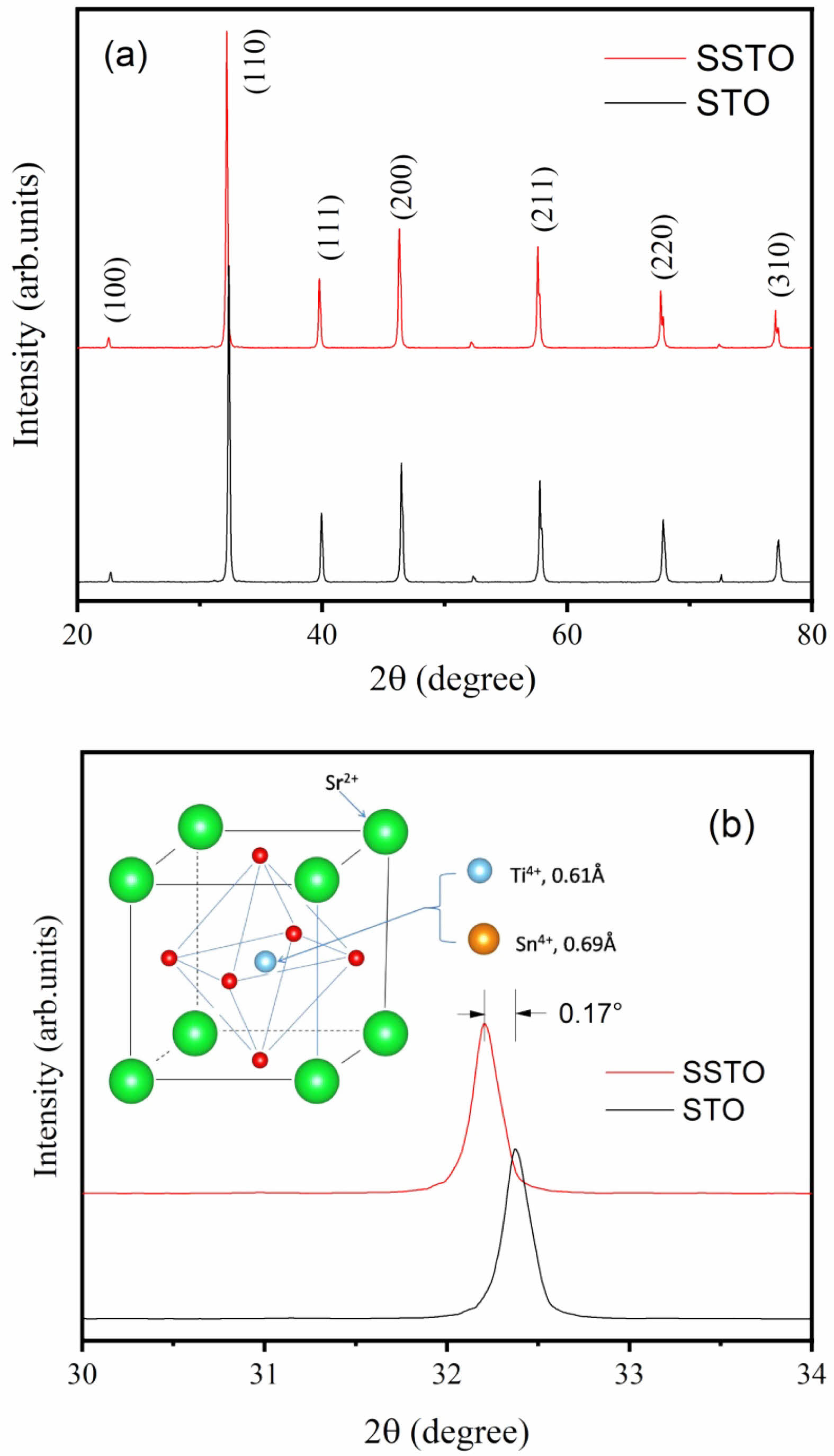
Figure 2 shows the frequency-dependent dielectric properties of the SSTO ceramics at low temperatures (300-100 K). It can be seen from Fig. 2(a) that the real part of the permittivity decreases with the increase of frequency, especially at temperatures of 300 K, 260 K, 140 K, and 100 K. This is because dipoles vary with the applied electric field and therefore have the greatest dipole polarization and a higher dielectric constant value in the low frequency domain. However, in the high frequency domain, the dipoles do not keep up with the frequency of the applied electric field, which means the dipoles lag behind the electric field. This results in low dipole polarization, which gives the dielectric constant a smaller value in the higher frequency domain. Figure 2(b) shows the variation of dielectric loss with the applied frequency. The values of tand develop in the same trend with that of e' in the frequency range of 100 Hz-1 MHz. The dielectric loss at room temperature is much higher than that at low temperatures. This result is believed to come from the formation of oxygen vacancies in SSTO ceramics because of the loss of oxygen in the process of sintering [11].
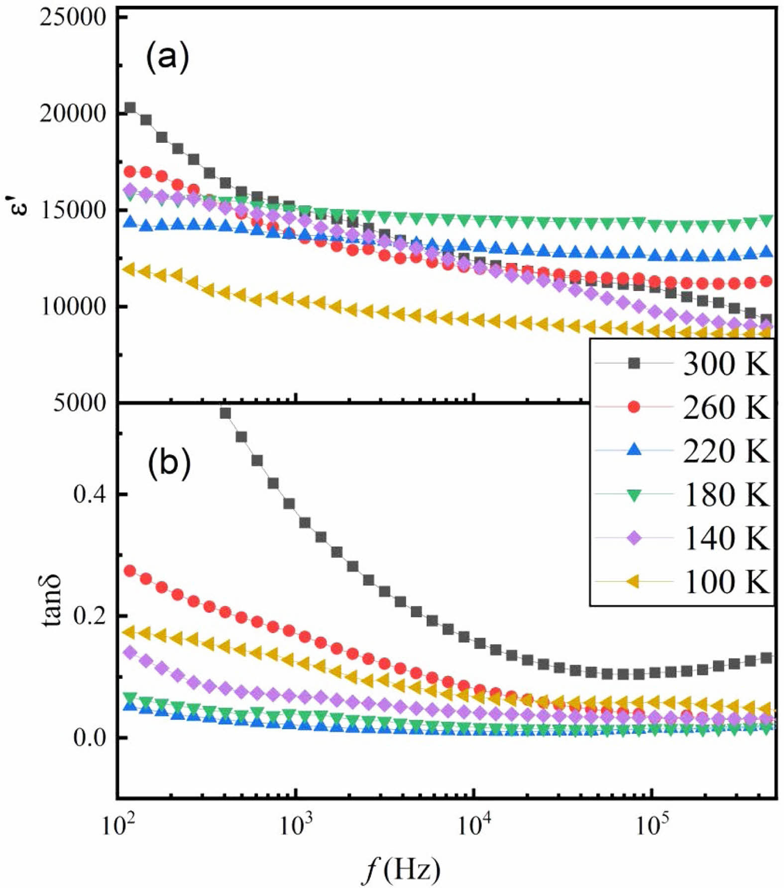
Figure 3 shows the variation of dielectric constant and loss with the temperatures at five typical frequencies (1 kHz, 10 kHz, 50 kHz, 100 kHz and 200 kHz) for SSTO sample. As shown in Fig. 3(a), the dielectric constant tends to be stable in the temperature region of 100~175 K, but varies greatly with frequency in the high-temperature region showing the dispersive characteristics. The main reason for this behavior is due to the polarization of charge carriers in the sample, which is known as Maxwell-Wagner polarization [12]. The strong low-frequency dispersion of dielectric constant can be divided into electronic, dipolar, interfacial and ionic polarization [13]. As shown in Fig. 3(b), the dielectric loss measured at different frequencies shows relaxation peaks at different temperatures. With the increase of frequency, the position of loss peak moves to higher temperature which is known as thermal activation process similar to Debye relaxation. This relaxation is attributed to the interfacial effect, which is affected by the oxygen vacancies at the grain boundaries.
Many factors have effects on the dielectric properties of oxide ceramics. In most cases, the dielectric behavior can be described by Universal Dielectric Responses (UDR) with the following equations [14],
where ε0 is the electric permittivity of free space, A, B and s are constants. In the case of UDR, the constant A represents the high-frequency dielectric response of the material, which is related to the polarizability of the material and reflects its ability to respond to an electric field at high frequencies. The constant B represents the low-frequency dielectric response of the material, which is related to the static or DC polarizability of the material and reflects its ability to store an electric charge. The constant s is a shape parameter that regulates the width of the dielectric response and reflects the relaxation time distribution in the material [15].
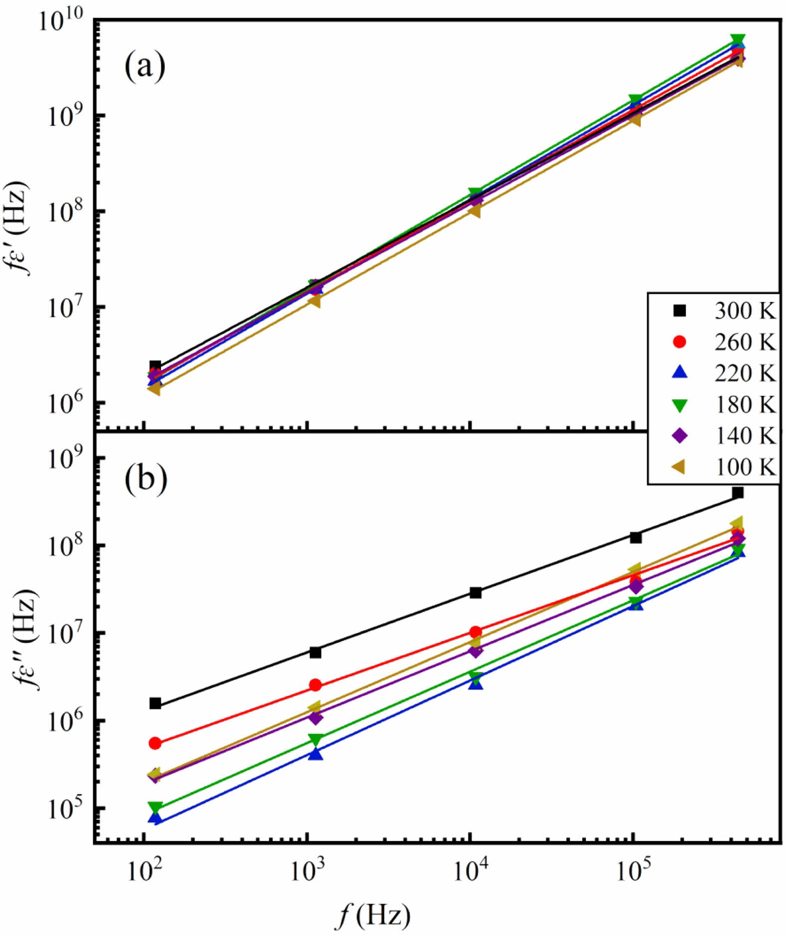
According to the equations (1) and (2), when the relationship between ln fε′ and ln f is plotted at given temperature, a straight line should be obtained. Similar linear relationship should be expected for ln fε′′ against ln f graph. Figure 4 shows the ln fε′-ln f and ln fε′′-ln f plots. Quite good straight lines with s = 0.1~0.8 are evident at a number of fixed temperatures, which means the dielectric behavior in SSTO ceramics is consistent with the UDR.
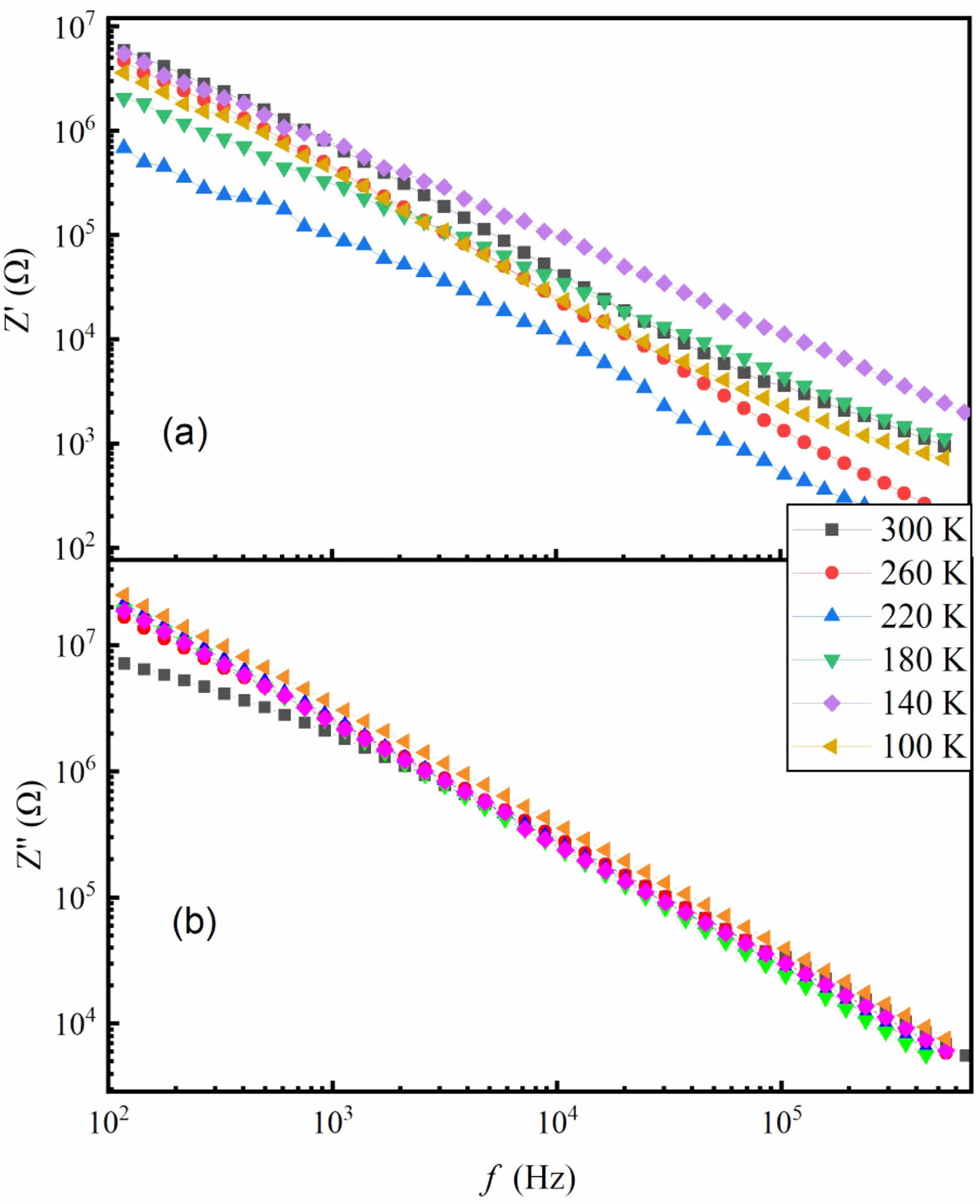
Figure 5 shows the frequency-dependent real part (Z') and imaginary part (Z") of impedance of the SSTO ceramics at different temperatures. It is clear that the values of Z' and Z" decreases with increasing frequency, which is consistent with the results of other oxide ceramics [16, 17]. The observed high values of Z' at low frequencies are mainly due to different structural effects, such as surface morphology, porosity, grain size and space charge polarization [18]. The small values of Z' in the high frequency region indicate the release of space charge polarization, which contributes to the reduction of barrier width and barrier performance. At different temperatures, Z" has a higher value in the low frequency domain, and the exhibits temperature-independent with the increasing of frequency suggesting the possible AC conductivity [19].
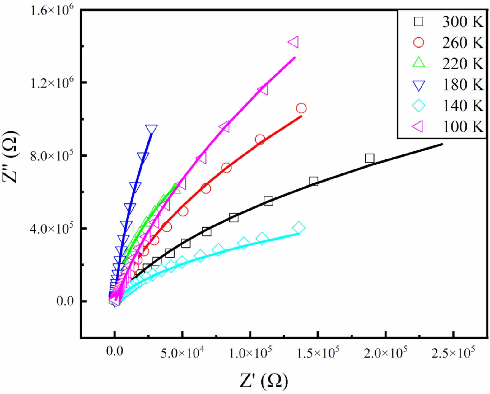
As is known, complex impedance spectroscopy (Nyquist plot) is a useful method to understand the contribution of grains and grain boundaries to the dielectric behavior at the microscopic level [20]. Because of the difference of relaxation time, the responses of grains and grain boundaries usually locate at different frequencies. Figure 6 shows the Nyquist plots of the fabricated SSTO ceramics at different temperatures. It is clear that Z'-Z" plots display typical semicircles with different radii, indicating the Debye relaxation occurs in SSTO ceramics. The semicircle in the impedance spectrum can be represented by a parallel combination of resistance and capacitance equivalent circuits or by a constant phase element (R-CPE) in series. The phase element (Q) of a constant is expressed as C = (R1−nQ)1/n, where n is the empirical exponent and its size ranges from 0 to 1 [21]. The solid lines in Fig. 6 show the fitting results with n = 0.3. By the theoretical fitting, the obtained grain resistance is about 2.4 MΩ at 300 K, and increases roughly to 13.6 MΩ when the temperature decrease to 100 K. The results suggest that the resistivity of the grains increases gradually with the decrease of temperature. The responses of grain boundaries are not shown in the Nyquist plots. Maybe the response frequency is not falling in our measuring frequency range.
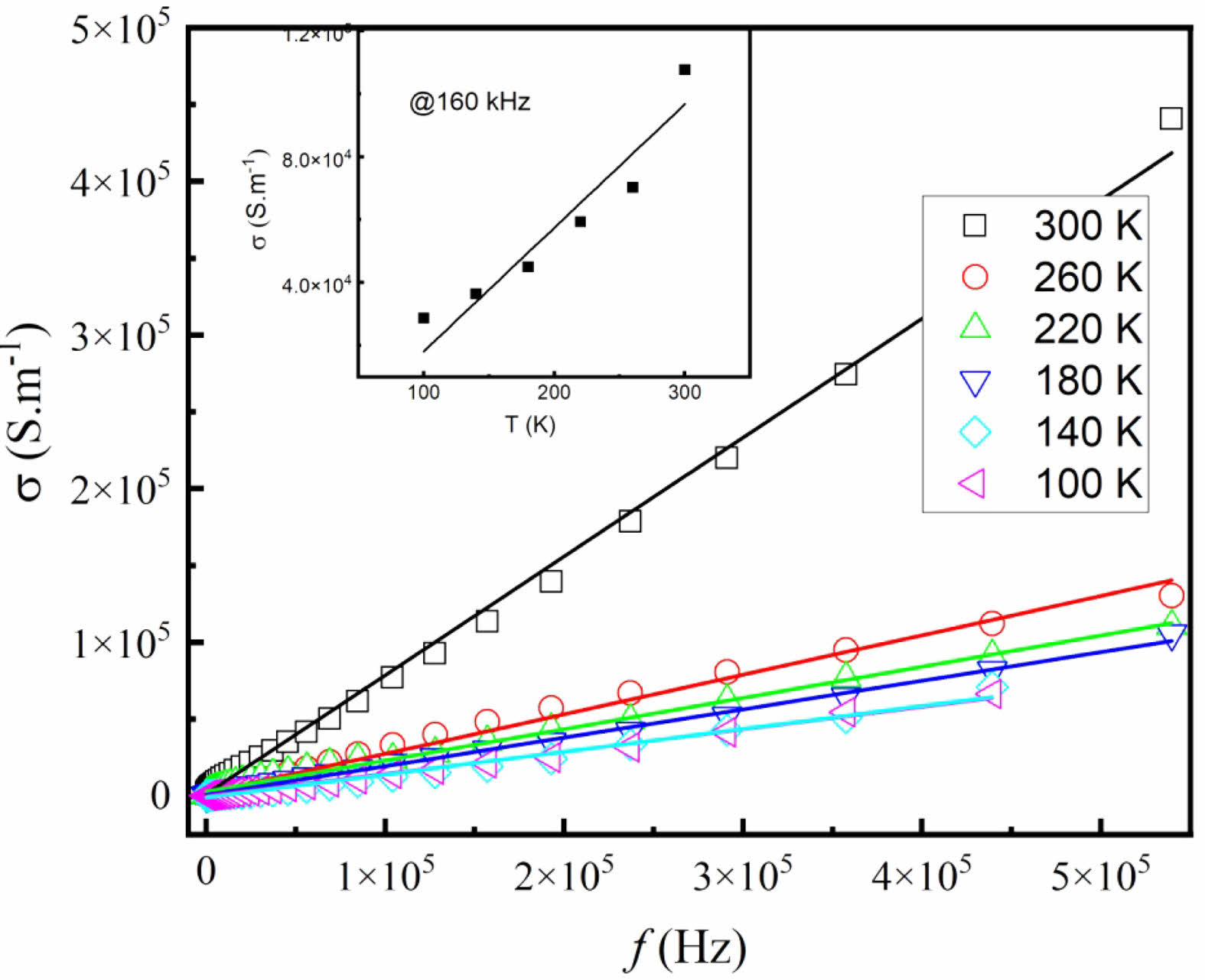
Figure 7 shows the electrical conductivity s of SSTO ceramics at different temperatures. The conductivity is obtained by using the of dielectric data with the formula [22],

The calculated values of σ at different temperatures are almost linearly increased with the increasing of frequencies. Moreover, as shown in the inset of Fig. 7, typical values of σ at fixed frequency f = 160 kHz increase linearly with increasing temperature, which is characteristic conductivity of semiconductors. The existing defects and oxygen vacancies in doped oxides are believed to be responsible for the results.
|
Fig. 1 (a) XRD patterns of the SSTO and STO ceramics. (b) Shift of (110) diffraction peak. Inset: schematic illustration of SSTO crystal structure. |
|
Fig. 2 Frequency dependence of (a) ε' and (b) tanδ of the prepared SSTO ceramics at different temperatures. |
|
Fig. 3 Temperature dependence of (a) ε' and (b) tanδ of the prepared SSTO ceramics at different frequencies. |
|
Fig. 4 Plots of (a) ln fε' vs. ln f and (b) ln fε′′ vs. ln f for the SSTO ceramics at some fixed temperatures. |
|
Fig. 5 Frequency dependence of the impedance (a) Z' and (b) Z'' of SSTO ceramics at different temperatures. |
|
Fig. 6 Nyquist plots of the SSTO ceramics at different temperatures. |
|
Fig. 7 Frequency dependence of electrical conductivity of the SSTO ceramics, the inset shows typical values of σ at a fixed frequency f = 160 kHz. The solid lines are the linear fits. |
In summary, cubic perovskite-type SSTO ceramics were fabricated by using a standard solid-state synthesis method. The low-temperature dielectric and impedance properties were studied in the frequency range of 100 Hz-1 MHz. Large dielectric permittivity and low dielectric loss were obtained for the sample. Development of grains with temperature was presented by using the complex impedance analysis. The conductivity investigation shows the semiconductor characteristic of the SSTO ceramics. Defects and oxygen vacancies produced during the fabrication process are responsible for the results.
- 1. M. Arshad, H.L. Du, M.S. Javed, A. Maqsood, I. Ashraf, S. Hussain, W.L. Ma, and H.P. Ran, Ceram. Int. 46[2] (2020) 2238-2246.
-

- 2. R. Brahem, N. Farhat, M.P.F. Graca, and L.C. Costa, J. Electron. Mater. 45[10] (2016) 5074-5081.
-
- 3. 3. E. Rocha-Rangel, J. Lopez-Hernandez, J.A. Rodriguez-Garcia, E.N. Armendáriz-Mireles, C.A. Calles-Arriaga, and W. Pech-Rodriguez, J. Ceram. Process. Res. 18[8] (2017) 590-593.
-
- 4. S. Yasmin, S. Choudhury, M. Hakim, A.H. Bhuiyanc, and M.J. Rahman, J. Ceram. Process. Res. 12[4] (2011) 387-391.
-
- 5. D.S. Krueger and S.J. Lombardoa, J. Ceram. Process. Res. 8[1] (2007) 31-37.
-
- 6. S.E. Leea, S.Y. Heoa, H.E. Goc, J.S. Leea, O.H. Kwonb, C. K. Hongc, H.J. Kimd, J.P. Hwangd, and Y.S. Ahna, J. Ceram. Process. Res. 19[4] (2018) 327-331.
-
- 7. J. Xie, H. Hao, H.X. Liu, Z.H. Yao, Z. Song, L. Zhang, Q. Xu, J.Q. Dai, and M.H. Cao, Ceram. Int. 42[11] (2016) 12796-12801.
-
- 8. R. Ganjir and P.K. Bajpai, J. Electron. Mater. 48[1] (2019) 634-641.
-
- 9. E. Jeong, S. Yu, J. Yoon, J. Bae, C. Cho, K. Lim, P. Borse, and H. Kim, J. Ceram. Process. Res. 13[5] (2012) 517-522.
-
- 10. B. Liu, C.C. Hu, Y.H. Huang, and K.X. Song, Mater. Lett. 253 (2019) 293-297.
-
- 11. B. Ullah, W. Lei, Q.S. Cao, Z.Y. Zou, X.K. Lan, X.H. Wang, and W.Z. Lu, J. Am. Ceram. Soc. 99[10] (2016) 3286-3292.
-
- 12. U. Kumar and S. Upadhyay, Mater. Lett. 227 (2018) 100-103.
-
- 13. P. Haldar, M. Laad, and S.R. Hassan, Phys. Rev. B 99[12] (2019) 125147.
-
- 14. U. Kumar, K. Ankur, D. Yadav, and S. Upadhyay, Mater. Charact. 162 (2020) 110198.
-
- 15. A.K. Jonscher, Nature 267[5613] (1977) 673-679.
-
- 16. P.G.R. Achary, S. Behera, R.N.P. Choudhary, and S.K. Parida, J. Mater. Sci.: Mater. Electron. 32[5] (2021) 5738-5754.
-
- 17. V.N. Thakur, A. Kumar, A. Kaushik, G.D. Gupt, and R.S. Dhaka, Mater. Res. Bull. 158 (2023) 112070.
-
- 18. G.R. Gajula, L.R. Buddiga, and M. Dasari, Results Phys. 18 (2020) 103196.
-
- 19. J. Fleig and J. Maier, J. Electrochem. Soc. 144[11] (1997) L302-L305.
-
- 20. D.C. Sinclair and A.R. West, J. Mater. Sci. 29[23] (1994) 6061-6068
-
- 21. J. Pradhan, H.K. Mallick, M.P.K. Sahoo, and A.K. Pattanaik, J. Mater. Sci.: Mater. Electron. 32[10] (2021) 13837-13849.
-
- 22. J.L. Qi, M.H. Cao, Y.Y. Chen, Z.C. He, C. Tao, H. Hao, Z.H. Yao, and H.X. Liu, J. Alloy. Compd. 772 (2019) 1105-1112.
-
 This Article
-
2023; 24(3): 583-587
Published on Jun 30, 2023
- 10.36410/jcpr.2023.24.3.583
- Received on Mar 23, 2023
- Revised on May 31, 2023
- Accepted on Jun 13, 2023
Services
Shared
Correspondence to
- Weitian Wang
-
School of Physics and Electronic Information, Yantai University, Yantai 264005, P.R. China
Tel : +86 13573512787 - E-mail: wtwang@ytu.edu.cn
Clean-Energy Research Institute(CRI), Hanyang University, 222, Wangsimni-ro, Seongdong-gu, Seoul, 04763, Korea
E-mail: jcpr@hanyang.ac.kr