


- Experimental investigation on the dielectric and impedance properties of indium doped titanium dioxide ceramics
Liqi Cui, Ruifeng Niu, Depeng Wang and Weitian Wang*
School of Physics and Electronic Information, Yantai University, Yantai 264005, P.R. China
This article is an open access article distributed under the terms of the Creative Commons Attribution Non-Commercial License (http://creativecommons.org/licenses/by-nc/4.0) which permits unrestricted non-commercial use, distribution, and reproduction in any medium, provided the original work is properly cited.
Single-phased indium doped titanium dioxide (Ti1-xInxO2, x=0~5%) ceramics were synthesized by using solid-state reaction method in this study. The doping effect on the dielectric and impedance properties was investigated in a broad frequency range from 102 Hz to 106 Hz. The observed dielectric behavior can be ascribed to the Universal Dielectric Response. In higher frequency field, the dielectric permittivity varies slightly with the doping concentration x. However, the measured dielectric constant increases significantly with the increase of doping concentration within lower frequency range. The charged grain-boundary cores originated from the doping trivalent ion can be used to explain the results
Keywords: Ceramics, Dielectric properties, Impedance analysis
Materials with colossal permittivity (CP > 103), low dielectric loss and good temperature and frequency stability have attracted considerable attention for smaller-size devices and supercapacitors applications [1]. There are currently a number of mechanisms used to explain the causes of high dielectric constants, leading to the discovery of new CP material. Firstly, BaTiO3-based ceramics, due to the internal barrier layer capacitance (IBLC) effect, have shown attractive CP characteristics [2]. However, these materials will go through ferroelectric-to-paraelectric phase transition with varying temperature, resulting in sudden changes in dielectric constants [3], which greatly limits the application range [4]. Although some studies have shown that the phase transition temperature can be moved by doping, the results still do not meet the requirements for the stability of dielectric materials in a wide temperature range [5, 6]. Secondly, CaCu3Ti4O12 (CCTO)-based CP materials show interesting temperature-independent dielectric behavior. At the same time, these materials usually have comparatively large dielectric losses due to the doped elements replacing Ti4+, resulting in a large number of free electrons generated in the lattice [7]. Finally, titanium dioxide (TiO2)-based materials exhibit a high dielectric constant and low dielectric loss without phase transition in a quite wide temperature range. Compared with other materials, TiO2 ceramics have the advantages of non-toxic, environment-friendly and low cost [8, 9]. Therefore, the synthesis of simple metal oxides TiO2 ceramics and studies on its dielectric and impedance properties are more meaningful.
In order to find high-performance dielectric materials, researchers have looked for possible reasons for the observed high dielectric constant. A large number of studies on doping modification of TiO2-based ceramics show that defects play an important role in dielectric behavior. In 2013, Hu proposed the electron pinning defect-dipole model (EPDD) to explain the origin of CP [10]. The results show that the donor and acceptor co-doping of TiO2 improves the dielectric properties [11]. It is believed the radius of the acceptor element in co-doped TiO2 ceramics has a key influence on the CP mechanism. Sheng Chao et al. found that a small amount doping of manganese can greatly improve its dielectric constant, while its dielectric loss can be reduced [12]. They analyzed the results and believed that the Ti4+ in TiO2 ceramics was partly replaced by Mn3+, thus forming electronic defects in the lattice. This defect can capture free electrons in ceramics to improve the dielectric constant. In addition, Nguyena et al. found that the doping of Mn4+ significantly changed the physical and chemical properties of TiO2 nanomaterials [13]. The microstructure and electrical properties of the TiO2 ceramics doped with different concentration of Ho3+ were reported by Feng et al. [14]. The results show that the electrical and dielectric properties of TiO2 are related to the trivalent ion doping concentration. As is known, stable defective compounds are more easily formed by doping acceptor elements with large ionic radius. However, trivalent cations with too large ion radius, such as Bi3+ and La3+, can more likely form substituted solid solution, which is easy to produce more impurity phases [15]. The impurity phase induces more free electrons, which deteriorate the dielectric properties by enhancing the interface polarization [16]. Therefore, the size of doped acceptor ions is very important for the dielectric properties. The radius of indium ion In3+ is 0.80 Å, which is smaller than that of Ho3+ (0.90 Å), and closer to that of Ti4+ (0.61 Å). As a result, In3+ can be used as a more suitable doping acceptor to improve the dielectric properties of TiO2 ceramics. Zhao et al. studied TiO2 ceramics doped with a series of A3+ receptors or B5+ donors to decode the effect of receptor and donor elements on the physical properties of TiO2 [17]. Albetran et al. studied the effect of In3+ doping on the phase transition of TiO2 nano-powder [18], and Khan et al. analyzed the effect of In3+ doping on the electronic structure and optical properties of TiO2 [19]. However, the dielectric properties of In3+ doped TiO2 with different concentrations have rarely been studied.
In this study, single-phased rutile indium-doped titanium dioxide TixIn1-xO2 ceramics were prepared by traditional solid-state-reaction method. The effects of the different doping concentrations of In3+ on the microstructure and dielectric properties of the obtained ceramic samples were studied. Temperature and frequency dependence of complex dielectric properties were measured. Impedance measurement in a wide frequency range is used to reveal the variation of grain and grain boundary with doping concentration.
The Ti1-xInxO2 ceramics were prepared by standard solid-state reaction method using TiO2 and In2O3 powders. The raw materials (purity: 99.95%, Macklin Chemical Co. Ltd.) are weighed and proportioned according to their stoichiometric ratio. The values of x were set as 0%, 0.5%, 1%, 3%, and 5%, and corresponding samples were named as IT00, IT05, IT10, IT30, and IT50, respectively. The mixed powders were ground in the agate grinding bowl container for 8 h and calcined at 1000 °C for 4 h in air. A thin disk with the diameter of 12 mm and thickness of approximately 5 mm was obtained by dry pressing at a pressure of 8 MPa. After sintered at 1200 ℃ for 6 h, Ti1-xInxO2 ceramic samples with bulk density greater than 95% were obtained. Both sides were polished and pasted with conductive silver paste as electrodes for dielectric measurement. The structure and phase composition of the synthesized Ti1-xInxO2 ceramics were characterized by using x-ray diffraction (XRD) with Cu Kα radiation. The complex dielectric responses were measured using a capacitor device over a temperature range of 80 to 300 K. An LCR meter (HIOKI-3532-50) was used to investigate the impedance spectrum in the frequency range of 102 Hz to 106 Hz.
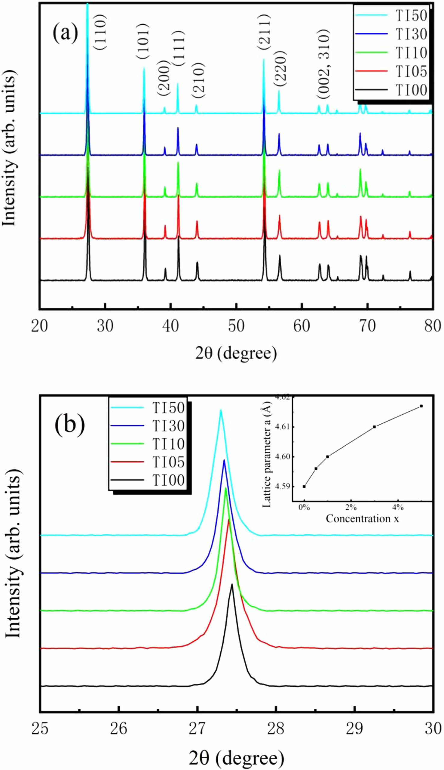
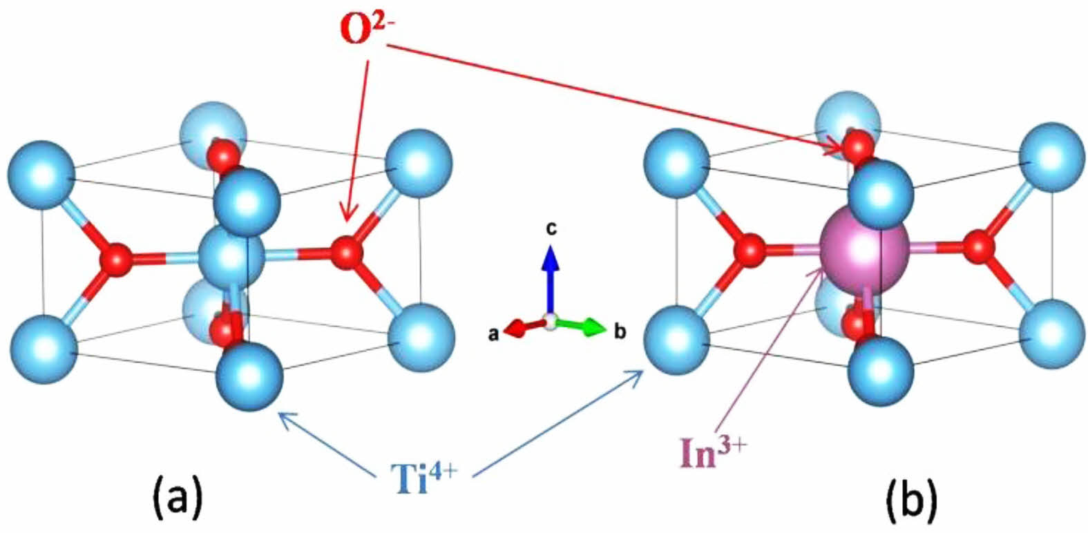
Figure 1(a) shows the typical θ-2θ XRD patterns of the fabricated Ti1-xInxO2 (x = 0%, 0.5%, 1%, 3%, and 5%) ceramics. All the samples exhibit an ideal tetragonal rutile structure (PDF#21-1276) with a P42/mnm space group, and no other impurity phases were identified. There was no obvious structure changed in TiO2 with the doping of In3+ up to 5% concentration. However, the position of diffraction peaks shifts to lower degree with the increasing concentration of In3+. Typical change of (110) peak is shown in Fig. 1(b). This shifting implies the increased lattice constant. Variation of the calculated lattice parameter a with the doping concentration x is shown in the inset of Fig. 1(b). As is known, the ionic radius of In3+ is larger than that of Ti4+. Doping with larger ions is responsible for the increased lattice constant. Schematic illustration of undoped and In3+ doped rutile TiO2 crystal structures is shown in Fig. 2.
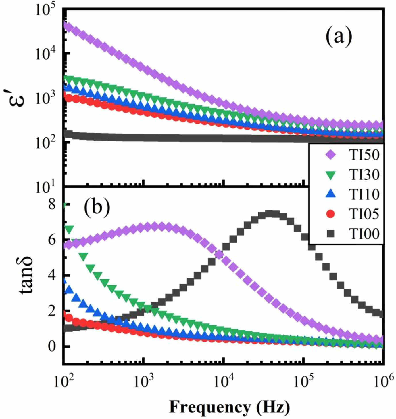
The dielectric permittivity and loss tangent are expressed by ε* = ε' + iε'' and tanδ = ε''/ε', where ε' and ε'' are the real and imaginary parts of the dielectric permittivity respectively. The frequency dependence of dielectric properties of the prepared samples at room temperature is shown in Fig. 3. It is obvious from Fig. 3(a) that the ε' value of undoped TiO2 at 103 Hz frequency is about 120 and the values do not vary much with frequency. With the doping of In3+, the values of ε' increased dramatically, especially in the lower frequency region. Except for TI50, all other samples exhibited a nondispersive dielectric constant of about 1000 at 300 K over the scanning frequency range of 102~106 Hz. The large ε' of TI50 observed at lower frequencies is attributed to the influence of space charge polarization, which will be discussed in detail later.
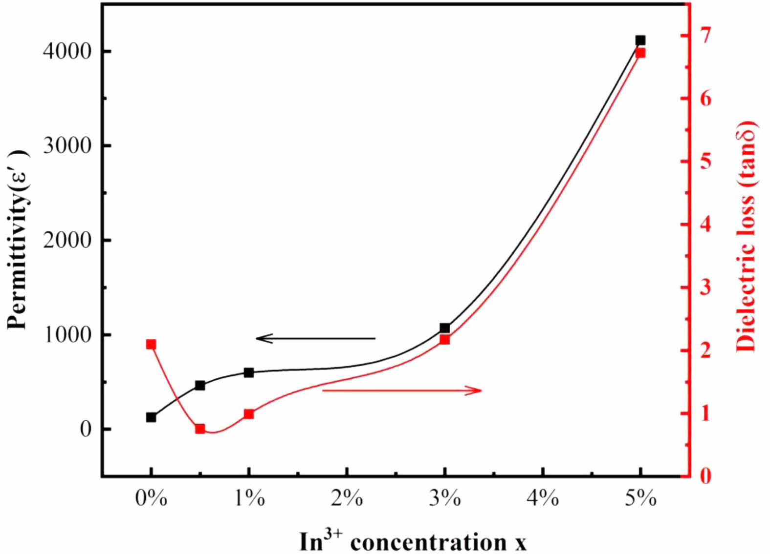
The variation of tanδ with the frequency is shown in Fig. 3(b). The curve of undoped TiO2 has a loss peak at 4×10⁴ Hz. It has been reported that tanδ value of TiO2 nanoparticles decreases and the loss peak shifts to the low-frequency region with the increase of the pressure of sample tablet pressing [20]. In addition to TI50, tanδ of the samples decreases gradually with increasing frequency up to 104 Hz and it is almost unchanged within the frequency range of 104~05 Hz. When the doping concentration increases, a loss peak is observed in TI50. The frequency position of the loss peak is similar to that observed for ε' in Fig. 3(a), which is a typical case that the polarization mechanism begins to decay because it cannot keep up with the frequency of the applied electric field. According to the measured frequency range and material type, the polarization mechanism is believed from the space charge polarization. As shown in Fig. 3(b), except TI00, the dielectric loss increases with the increase of In3+ doping concentration. At 105 Hz, the values of tanδ of IT05, IT10, IT30 and IT50 are 0.26, 0.3, 0.37 and 1.43 respectively. As is known, the hole density in Ti1-xInxO3 will increase with the increasing doping of trivalent In ions. The resulting dominant conduction process is responsible for the observed dielectric loss. In the case of Mn3+ and Ta5+ doped TiO2, similar results were observed for dielectric loss [12, 21]. The developing trend of ε' and tanδ with the In3+ doping concentration is illustrated in Fig. 4.
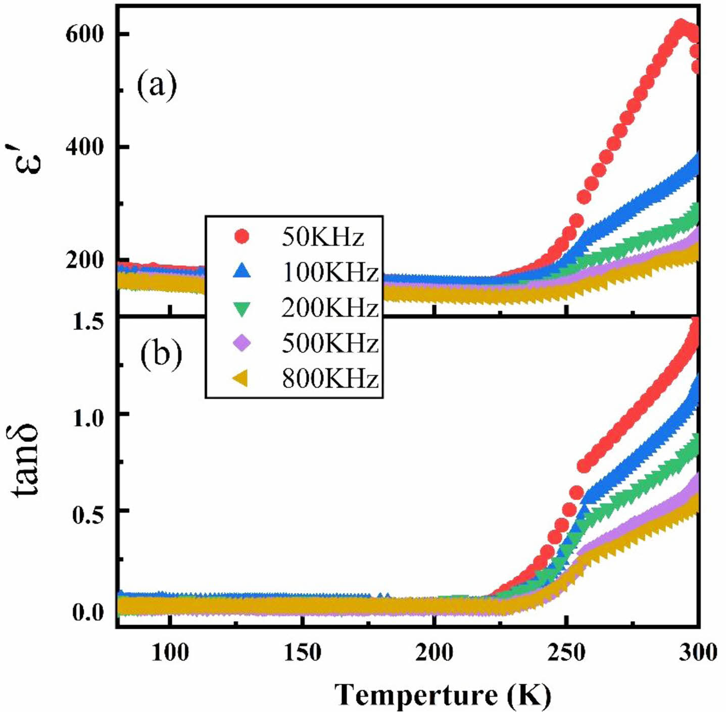
Compared with other samples, there is a significant increase of ε' and tanδ for TI50. Typical temperature dependence of dielectric permittivity for TI50 is shown in Fig. 5. It is found that the value of ε' is almost constant at up to 250 K and increases dramatically with further increase of temperature [Fig. 5(a)]. A similar developing trend was found in tanδ [Fig. 5(b)]. Large values of tanδ at higher temperature may be from the increase of electronic conduction originating from the thermal activation of electrons. Similar properties have been reported earlier for Sr(Gd0.5Nb0.5O3) oxides [22]. At high temperature (T > 225 K), the dielectric constant and dielectric loss decrease with the increase of frequency, while the material shows good temperature stability from 50 kHz to 800 kHz at low temperature. Generally, with the increase of frequency, many polarization mechanisms cannot keep pace with frequency. Therefore, their contribution to the overall polarization intensity and dielectric constant will be reduced.
It is well known that the increasing background in the dielectric loss means that the background is related to the jump conductivity caused by charge carriers. This behavior is called Universal Dielectric Response (UDR) by Jonscher [23, 24]. According to this model, ε' and ε′′ can be expressed as,

where ε∞ is the high-frequency value of ε′(ω), ε0 is the electric permittivity of free space, A and s are constants, and ω = 2πf is the angular frequency.
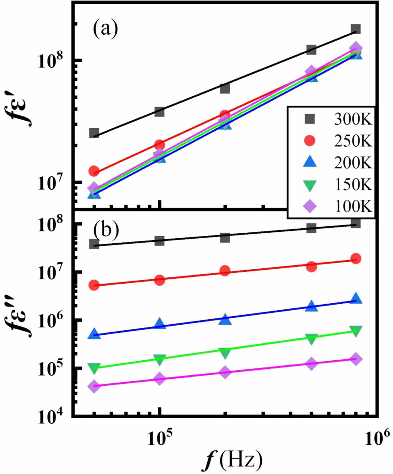
According to the UDR, when log fε′ vs. log f and log fε′′ vs. log f are plotted at given temperatures, straight line with a slope of s should be obtained. Figure 6 shows the logfε′-logf and logfε′′-logf graph. Quite good straight lines are obtained in Fig. 6 for the logf dependence of log fε′ with s=0.71~0.8 and log fε′′ with s=0.1~0.3, which is consistent with Jonscher’s assumption [24].
The increase of dielectric constant of Ti1-xInxO3 is attributed to the generation of electron traps, which can be expressed as,

When the doping concentration of In3+ increases, it is expected that In3+ ions will gather at the grain boundary because of the driving force of electrostatic force and elastic strain energy. Therefore, the negatively charged grain-boundary cores will be produced due to the charged defects In'Ti. Because the positive space charge layer near the electron depletion region balances a large number of In3+ sites to separate and replace Ti4+ sites, a back-to-back Schottky barrier is formed [25, 26].
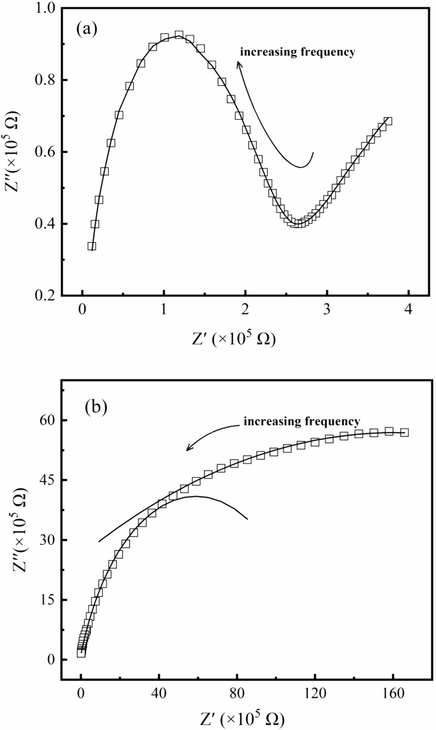
In order to understand the contribution of grains and grain boundaries to the dielectric effect in the prepared samples, complex impedance spectroscopy has been carried out. Complex impedance spectroscopy is a useful method to study the dielectric behavior of materials at the microscopic level [27]. Generally speaking, the complex impedance spectrum (i.e. Nyquist diagram) is composed of two half arcs, and the position of the arcs depends on the relaxation time. As the relaxation time of grains is shorter than that of grain boundaries, the arc corresponding to the grain effect locates at the higher frequency, while that corresponding to the grain boundary effect locates at the lower frequency.
By using complex impedance analysis, typical Nyquist plots for TI50 at 300 K and 260 K in the frequency range of 102 Hz~106 Hz are shown in Fig. 7. Two semi-arcs corresponding to the grain and grain boundary can be observed. The grain and grain boundary resistance of TI50 at different temperatures can be obtained by the theoretical fits. At 300 K, the grain resistance is about 1.19×10⁵ Ω, and the grain boundary resistance is about 4.89×10⁵ Ω. At 260 K, the grain and grain boundary resistances are about 6.32×10⁶ Ω and 4.35× 10⁷ Ω, respectively. The grain and grain boundary resistances increase greatly with the decrease of temperature. Similar results for the other samples can be obtained by the same analysis. The existing grain and grain boundary help to form the charged grain-boundary cores, which contributes to enhance the dielectric permittivity of the Ti1-xInxO3 ceramics with the increase of In3+ doping concentration x.
|
Fig. 1 (a) XRD patterns of the prepared samples. (b) Shift of (110) diffraction peak. Inset: variation of the lattice parameter α with the doping concentration x. |
|
Fig. 2 Schematic illustration of (a) undoped and (b) In3+ doped rutile TiO2 crystal structures. |
|
Fig. 3 Frequency dependence of (a) ε' and (b) tan δ of the prepared samples at room temperature. |
|
Fig. 4 Permittivity and dielectric loss of Ti1-xInxO2 ceramics with different x measured at 1 kHz and 25 ℃. |
|
Fig. 5 Temperature dependence of (a) ε' and (b) tanδ for sample TI50. |
|
Fig. 6 The log-log plots of the frequency dependence of (a) fε' and (b) fε'' of TI50 at given temperatures. The solid lines are the linear fittings. |
|
Fig. 7 Nyquist plots for sample TI50 at (a) 300 K and (b) 260 K, the solid lines are the theoretical fits. |
In short, a series of single-phased In3+ doped TiO2 samples with different concentrations were prepared through a standard solid-state synthesis method. The dielectric properties were investigated as functions of frequency and temperature. The observed dielectric behavior can be explained by using the Universal Dielectric Response. The grain and grain boundary effects were studied by using the complex impedance analysis. The measured dielectric constant of the prepared Ti1-xInxO2 ceramics increases with the increase of doping concentration x, and the highest dielectric constant has been obtained for the sample Ti0.95In0.05O2 at room temperature. It is assumed that the charged grain-boundary cores are responsible for the enhancement of the dielectric constant of Ti1-xInxO2.
This work was supported by the Graduate Innovation Foundation of Yantai University (No. KGIFYTU2212).
- 1. C. Moure and O. Peña, Prog. Solid State Chem. 43[4] (2015) 123-148.
-

- 2. C. Pecharromán, F. Esteban‐Betegón, J. Bartolomé, S. López‐Esteban, and J. Moya, Adv. Mater. 13[20] (2001) 1541-1544.
- 3. O. Thakur, C. Prakash, and D. Agrawal, J. Ceram. Process. Res. 3[2] (2002) 75-79.
- 4. X.-G. Zhao, P. Liu, Y.-C. Song, A.-P. Zhang, X.-M. Chen, and J.-P. Zhou, Phys. Chem. Chem. Phys. 17[35] (2015) 23132-23139.
-
- 5. R. Islam, S. Choudhury, S. Rahman, and M.J. Rahman, J. Ceram. Process. Res. 13[3] (2012) 248-251.
-
- 6. S. Yasmin, S. Choudhury, M. Hakim, A. Bhuiyan, and M. Rahman, J. Ceram. Process. Res. 12[4] (2011) 387-391.
-
- 7. X.W. Wang, P.B. Jia, X.E. Wang, B.H. Zhang, L.Y. Sun, and Q.B. Liu, J. Mater. Sci.: Mater. Electron. 27[11] (2016) 12134-12140.
-
- 8. W. Zhou, M. Cao, H. Wang, H. Hao, Z. Yao, and H. Liu, Ceram. Int. 48[12] (2022) 16723-16729.
-
- 9. L. Cui, R. Niu, and W. Wang, J. Ceram. Process. Res. 23[1] (2022) 57-61.
-
- 10. W. Hu, Y. Liu, R.L. Withers, T.J. Frankcombe, L. Norén, A. Snashall, M. Kitchin, P. Smith, B. Gong, H. Chen, J. Schiemer, F. Brink, and J. Wong-Leung, Nat. Mater. 12[9] (2013) 821-826.
-
- 11. Z. Wang, H. Chen, W. Nian, J. Fan, Y. Li, and X. Wang, J. Alloys Compd. 777 (2019) 317-324.
-
- 12. S. Chao and F. Dogan, J. Am. Ceram. Soc. 94[1] (2011) 179-186.
-
- 13. H.H. Nguyena, G. Gyawali, and B. Joshi, J. Ceram. Process. Res. 23[1] (2022) 33-40.
-
- 14. F. Peng and D. Zhu, Ceram. Int. 44[17] (2018) 21034-21039.
-
- 15. Y. Yu, W.-L. Li, Y. Zhao, T.-D. Zhang, R.-X. Song, Y.-L. Zhang, Z.-Y. Wang, and W.-D. Fei, J. Eur. Ceram. Soc. 38[4] (2018) 1576-1582.
-
- 16. Z. Cao, J. Zhao, and J. Fan, Ceram. Int. 47[5] (2021) 6711-6719.
-
- 17. H.M. Albetran and I.M. Low, Arab. J. Chem. 13[2] (2020) 3946-3956.
-
- 18. C. Zhao, Z. Li, and J. Wu, J. Mater. Chem. C 7[14] (2019) 4235-4243.
-
- 19. M. Khan, Z. Lan, and Y. Zeng, Materials 11[6] (2018) 952.
-
- 20. T. Ji, Y. Gao, T. Qin, D. Yue, H. Liu, Y. Han, and C. Gao, J. Phys. Chem. C 125[6] (2021) 3314-3319.
-
- 21. P. Anithakumari, B.P. Mandal, S. Nigam, C. Majumder, M. Mohapatra, and A.K. Tyagi, New J. Chem. 41[21] (2017) 13067-13075.
-
- 22. P. Kumar, A.K. Sharma, B.P. Singh, T.P. Sinha, and N.K. Singh, Physica B 403[1] (2010) 103-108.
- 23. A.K. Jonscher, Dielectric Relaxation in Solids (Chelsea Dielectrics, London, 1983).
- 24. A.K. Jonscher, Nature 267[5613] (1977) 673-679.
-
- 25. Q. Wang, O. Varghese, C.A. Grimes, and E.C. Dickey, Solid State Ionics 178[3] (2007) 187-194.
-
- 26. X. Guo and J. Maier, J. Electrochem. Soc. 148[3] (2001) E121.
-
- 27. D.C. Sinclair and A.R. West, J. Mater. Sci. 29[23] (1994) 6061-6068.
-
 This Article
-
2023; 24(2): 348-352
Published on Apr 30, 2023
- 10.36410/jcpr.2023.24.2.348
- Received on Nov 17, 2022
- Revised on Jan 19, 2023
- Accepted on Jan 27, 2023
Services
- Abstract
introduction
experimental procedure
results and discussions
conclusion
- Acknowledgements
- References
- Full Text PDF
Shared
Correspondence to
- Weitian Wang
-
School of Physics and Electronic Information, Yantai University, Yantai 264005, P.R. China
Tel : +86 13573512787 Fax: +86 535 6901947 - E-mail: wtwang@ytu.edu.cn
Clean-Energy Research Institute(CRI), Hanyang University, 222, Wangsimni-ro, Seongdong-gu, Seoul, 04763, Korea
E-mail: jcpr@hanyang.ac.kr