


- Impact of CIGS, CdS and i – ZnO film thickness, temperature on efficiency enhancement of CIGS solar cells
Deepa Lakshmi.Ba, Rajendran RSb, Jackrit Suthakornc and Branesh M. Pillaic,*
aDepartment of Electrical and Electronics Engineering, Ramco Institute of Technology, Tamil Nadu
bAAA Enterprisers, Coimbatore, 600098, Tamil Nadu
cCenter for Biomedical and Robotics Technology, Faculty of Engineering, Mahidol University, ThailandThis article is an open access article distributed under the terms of the Creative Commons Attribution Non-Commercial License (http://creativecommons.org/licenses/by-nc/4.0) which permits unrestricted non-commercial use, distribution, and reproduction in any medium, provided the original work is properly cited.
In an attempt to enhance solar light photon to electron transformation proficiency of copper indium gallium selenide (CIGS) solar cells, computational exploration has been accomplished through numerical simulation. The SCAPS program was utilized to simulate enactment of CIGS. The electrical, optical properties of CIGS such as band diagram, current density, recombination current, IPCE and current – voltage efficiency was analyzed. The electrical, physical properties, thicknesses of individual layers comprising CIGS, CdS and ZnO were optimized along with their operating temperature. The CIGS solar cell efficiency analysis was executed and analyzed in the AM1.5 spectrum. The depth of CIGS, CdS and ZnO layers in CIGS solar cell determines the efficiency. The simulated optimization of CIGS properties is encouraging for enhancing the CIGS solar cell proficiency
Keywords: CIGS solar cells, SCAPS, CdS and ZnO layers, IPCE
Solar energy, a potential renewable energy can ameliorate the energy crisis of the globe. The growth, need for photovoltaic device market is exponential at present. The silicon based first generation solar cells are highly efficient, needs advanced fabrication techniques and very expensive [1-5]. The second-generation solar cells constructed on copper indium gallium diselenide alloys (CIGS) are encouraging due to good stability, cost effective, manufacturing flexibility and long-life time etc. [6-9]. CIGS has attained high conversion efficiency due to suitable band gap, high absorption coefficient etc. CIGS has shown 23.4% efficiency and well behind the Shockley-Queisser limit [10, 11]. Hence, reducing thickness of CIGS absorber coating reduces indium and gallium quantity and cost [12, 13]. This aims to develop low cost CIGS and to improve the efficiency by means of doping, apt thicknesses of functional layers, modifying the CIGS structure and suitable layer materials etc. [14, 15]. To improve the efficiency of CIGS, numerous thicknesses of CIGS absorber layer, ZnO and CdS were explored. The electrical, optical properties and efficiency of the predicted CIGS structures were numerically investigated and improved the CIGS performance. In modified CIGS structure, CIGS absorber layer, ZnO and CdS was varied much to investigate their performance to optimize the CIGS solar cells. The current density of electrons and holes, generation, recombination currents, current – voltage behavior and incident photon to electron conversion efficiency etc., were analyzed thoroughly. The operating temperature of CIGS, thicknesses of CIGS absorber coating, ZnO and CdS influences the optical, electrical and efficiency characteristics the solar cell remarkably. From these investigations, an optimized structure with CIGS thickness of 1.5 μm, CdS with 0.07 μm depth, an i-ZnO film with 0.07 μm thickness has upgraded effectiveness of CIGS. CIGS with these improved features has shown the efficiency of 11.54%. Hence, the performance parameters varied in this research are capable of generating better efficiency in comparison with conventional CIGS solar cells.
Numerical simulation of CIGS is accomplished by dint of employing the SCAPS-1D program (version 3.3.02) under the standard solar irradiation spectrum AM1.5 Global conditions and with incident light power of 1000 W/m2.
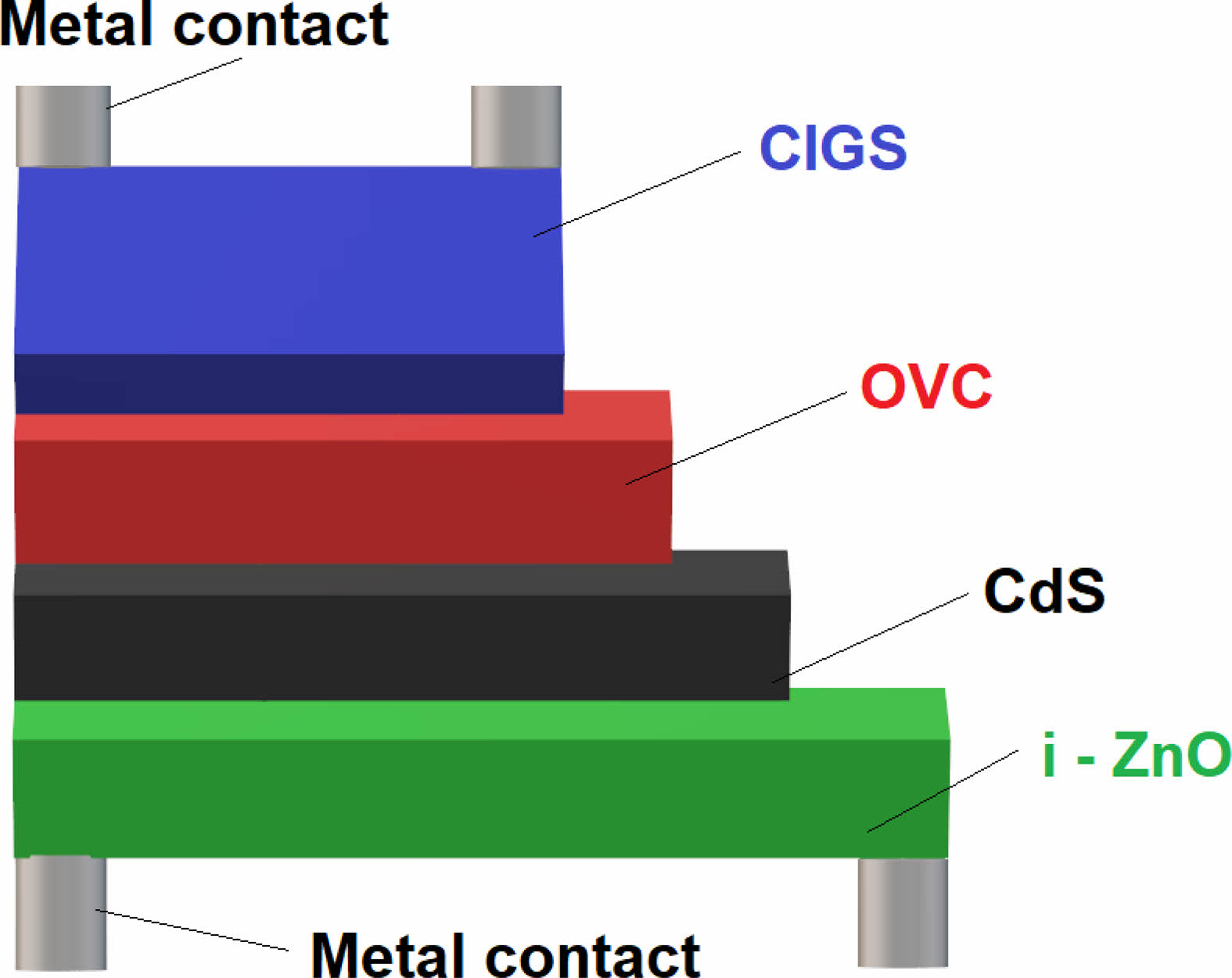
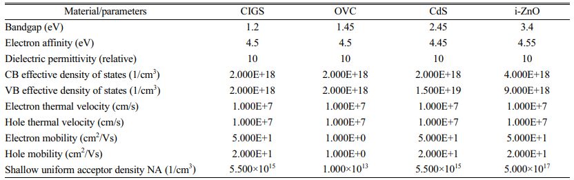
This SCAPS-1D program mathematically utilizes Poisson equation, holes continuity equation and electron continuity equation for determining the semiconductor behavior. The studied CIGS structure is depicted in Fig. 1. And, physical factors of all layers used in the program are presented in Table 1.
CIGS device modeling, its performance with the varied thicknesses of individual layers containing CIGS, CdS and ZnO thin films have been explored along with various operating temperature. The main emphasis is to optimize proficiency of CIGS.
Fundamental SCAPS semiconductor relations are, [16, 17].
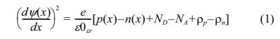
Where ψ(x) is electrostatic potential, e is electrical charge, εr and ε0 are relative permittivity, permittivity of free space, p(x) and n(x) are hole, electron concentration, ND is donor charge impurity and NA is acceptor nature, ρp and ρn are holes and electrons dissemination correspondingly [18].
The electrons, holes continuousness equivalences are,
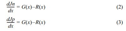
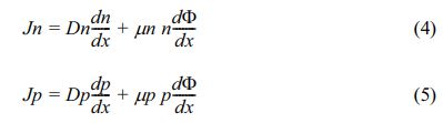
Where Jn, Jp are electron, hole current densities, G(x), R(x) are recombination, generation proportion. Drift, diffusion carrier transportation equalities are,
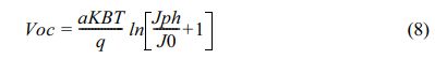
The current and voltage relationship is obtained from,

Where, q is charge, Jph is photocurrent density, T is temperature, J0 is saturation current density, KB is Boltzmann constant and ‘a’ is ideality factor.
Jsc is directly related to quantity of photons absorbed by the cell.
In Jsc, V = 0 and (6) provides,

The Voc is supreme V at zero current of a solar cell.
The fill factor (FF) is,

|
Fig. 1 Structure of the CIGS cell. |
Impact of band offset
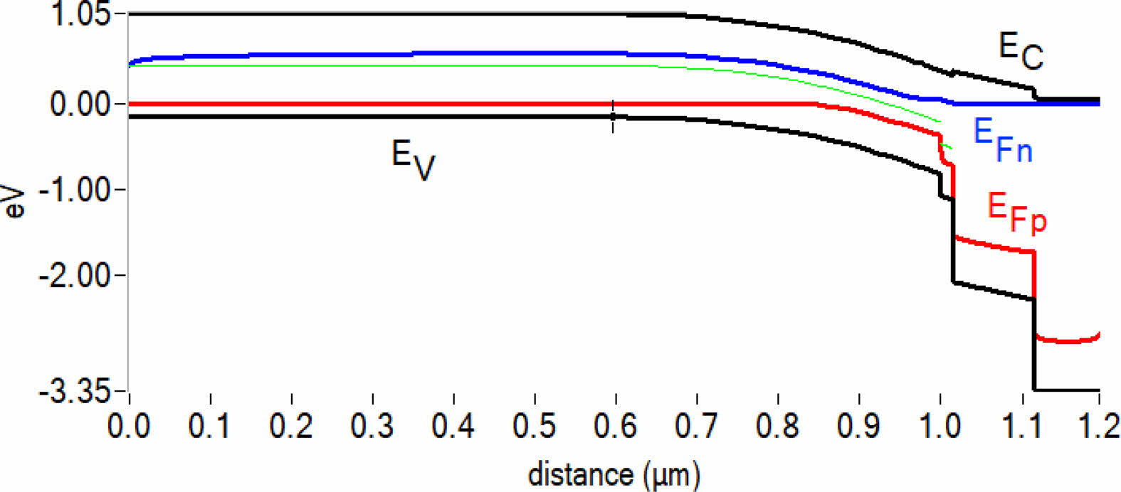
From Anderson's rule, the energy band chart formed between hetero junctions by of semiconductor ought to be aligned [19]. The configuration activates incoherence at interface. Band chart of proposed CIGS with band offset at boundary is illustrated in Fig. 2. Bandgap of CIGS is 1.12 eV, CdS is 2.4 eV and 3 eV for i-ZnO.
SCAPS program estimates recombination, current density, band diagram and carrier transport. In the CIGS cell, the customary thermal velocities of holes, electrons are 1 × 107 cm/s, interface defect is 1 × 109 cm3 to 1 × 1013 cm3 with 0.1 eV interface gap.
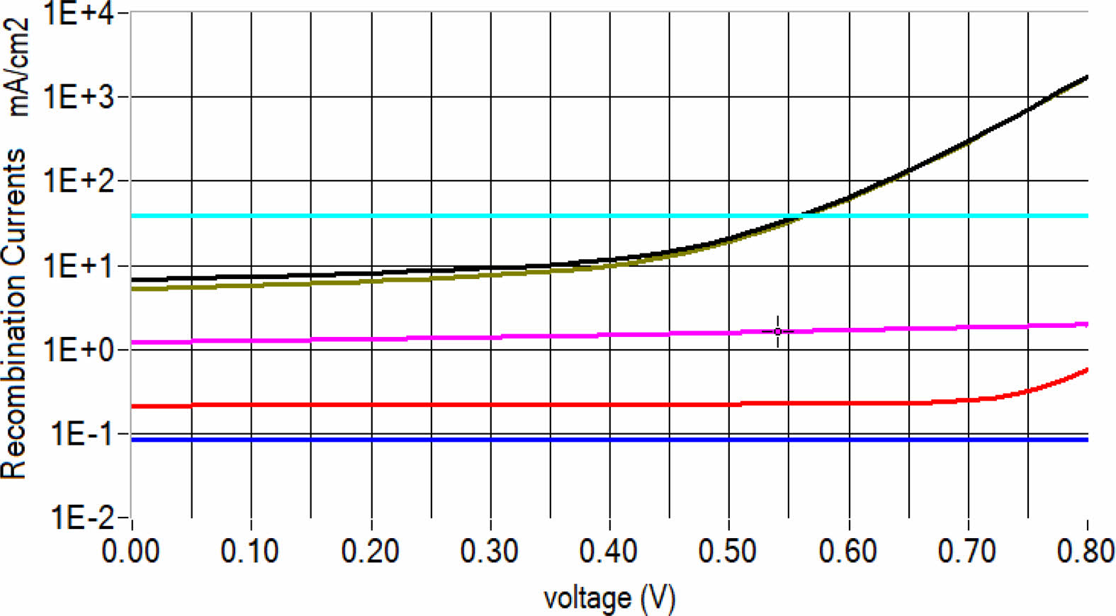
Generation-recombination and current density
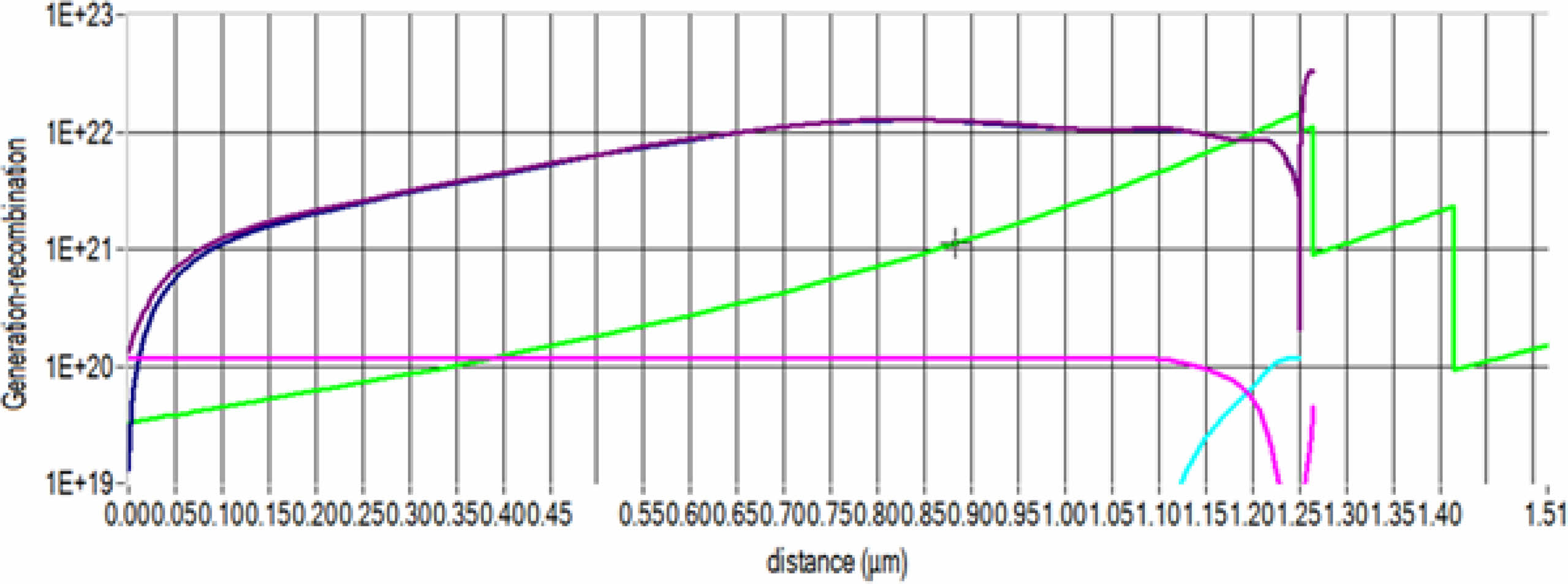
The carrier generation process creates the electron-hole pairs by excitation. In the recombination process recombines, annihilates the electrons and holes from conduction, valence band respectively. In CIGS semiconductors, the vital methods are optical, Shockley-Read-Hall, Auger and impact ionization which lead to generation, recombination. The recombination behavior of predicted CIGS is depicted in Fig. 3.
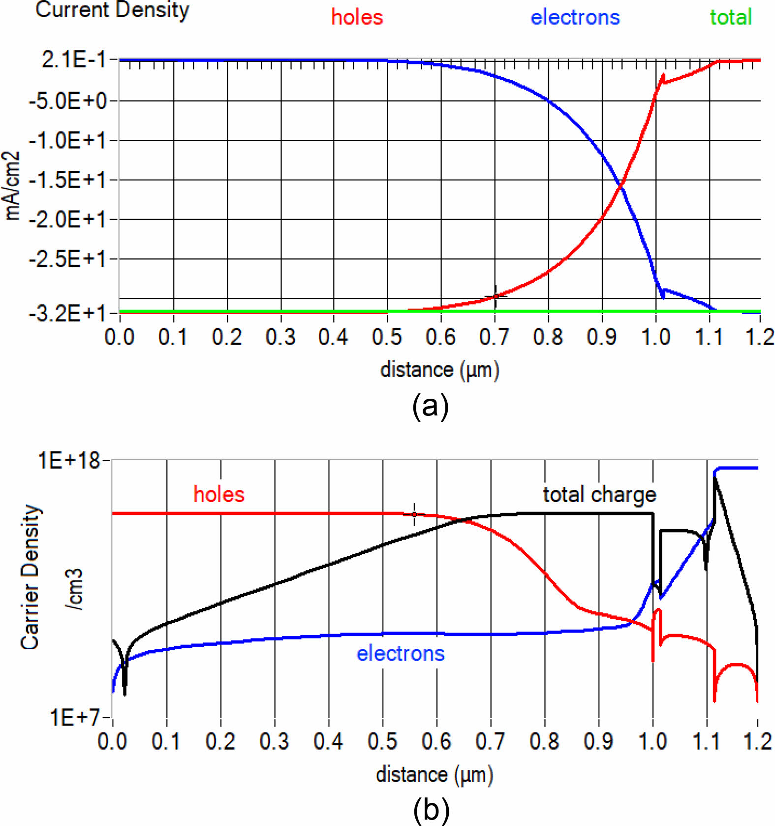
Current density characteristics CIGS under dark or without illumination is portrayed in Fig. 4(a). As the distance increases to 0.6 μm, the number of holes begins to increase and the electron density decreases. Their numbers are exactly same at 0.95 μm and they continue their trends. The current density characteristics of CIGS after illumination are depicted in Fig. 4(b). The light photons trigger more electron, hole charge than in the previous case. The overall current density has raised and will influence the photon to electron conversion efficiency.
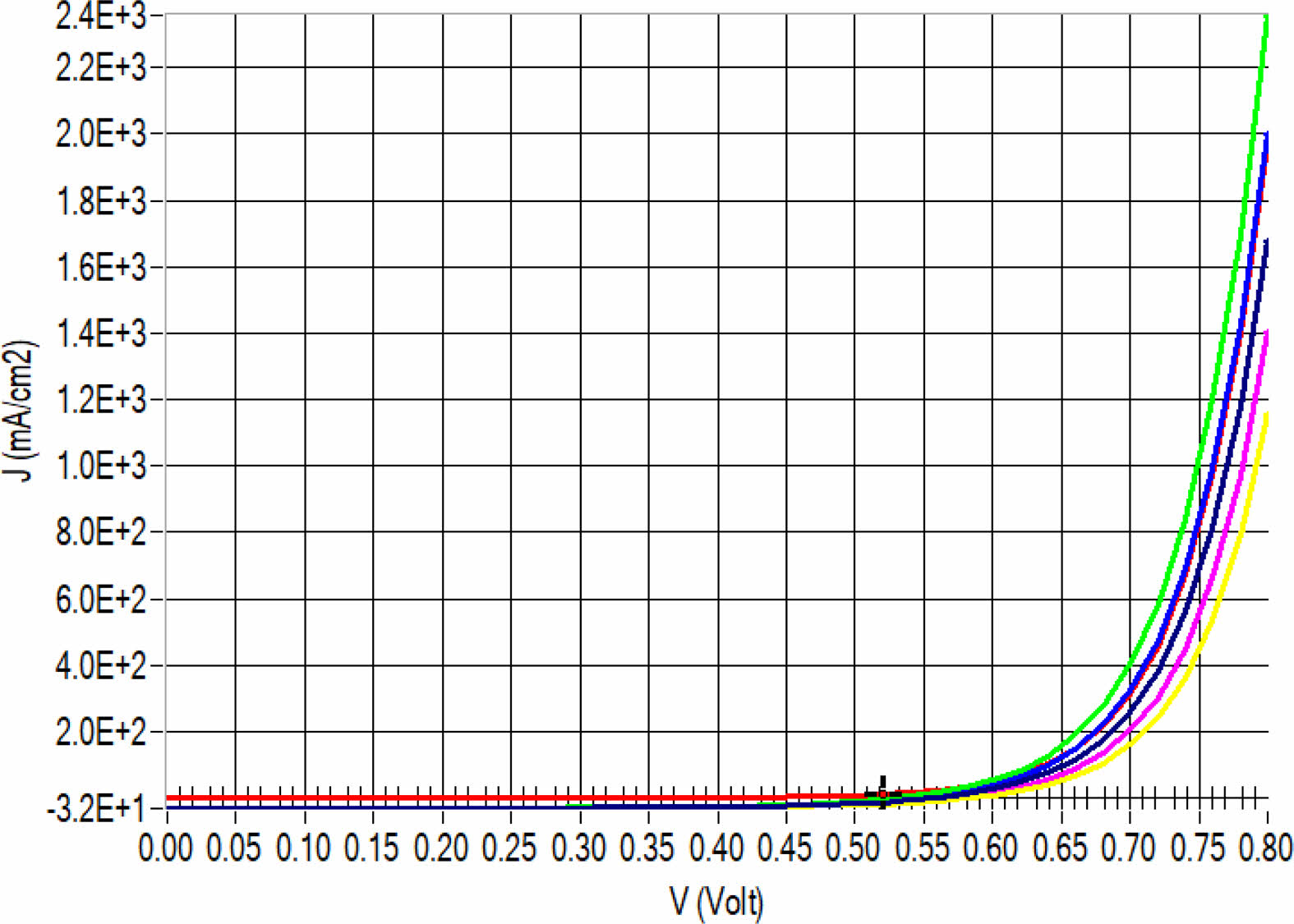
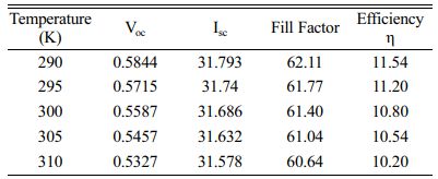
Outcomes of operating temperature on CIGS
The efficiency of CIGS and its dependence on operating temperature are studied. This is significant in taking the global market as they are exposed to wide range of temperatures [20]. The temperature influences the performance of CIGS parameters, Voc, Jsc, FF and efficiency [21, 22]. The variations of these parameters as function of temperature range of 290 k to 310 k are presented in Table 2. The Voc declines with rising temperature as Voc hinge on saturation current and declines swiftly with growing temperature. And, proficiency of CIGS also keeps on decreasing with respect to increase in temperature as exposed in Fig. 5. The recombination Current as a function of temperature is shown in Fig. 6. When the operating temperature is raised, the Voc, Jsc, FF and efficiency etc., are affected which lowers the efficiency of CIGS [23, 24]. The optimum efficiency was observed in the 290 k operating temperature with 11.54% efficiency for CIGS solar cell. For the remaining temperatures increased of the order of 5 k, regular decrease in efficiency was observed.
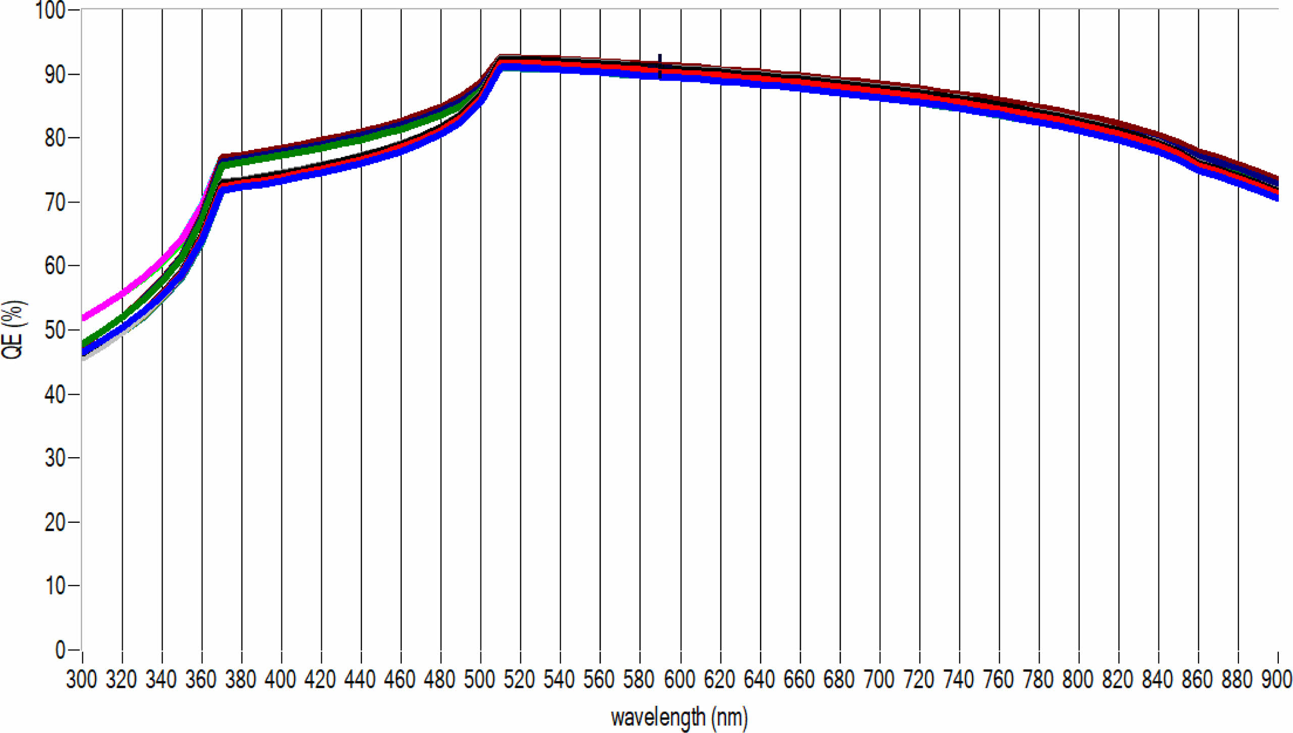
Incident photon to electron conversion efficiency (IPCE)
The IPCE is effective electrons excited by photons from CIGS solar cell and incident photons from light source. This external quantum efficiency is 1 (100%) if entire photons create electron-hole pairs for a particular wavelength. The variable CIGS thicknesses, CdS, i-ZnO layer thickness and IPCE etc., influence the efficiency. The IPCE behavior of CIGS as a function of temperature is presented in Fig. 7. With respect to the rise in operating temperature, IPCE changed marginally.
Role of CdS buffer layer thickness
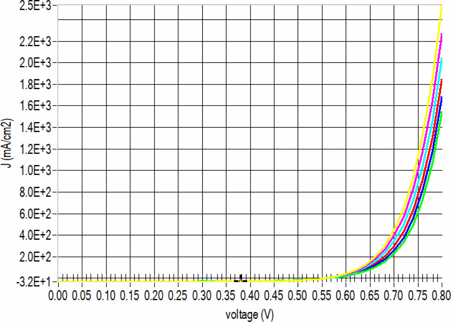
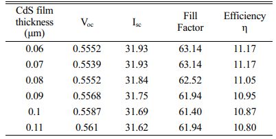
CdS buffer deposit in CIGS structure has been researched and positively influence competence. The CdS buffer layer in CIGS solar cell assembly increases the short-circuit current density (Jsc). Variations of Voc, Jsc, FF, efficiency due to CdS buffer layer breadth in CIGS is deposited in Table 3. The optimum CdS buffer layer is determined as 0.06 µm to attain the CIGC efficiency of 11.17% with a fill factor of 63.14. The 0.11 µm CdS layer thickness has recorded the least efficiency among the tested CIGS solar cells as 11.05% with 62.52 as fill factor. The efficiency performance due to the variation of CdS layer in CIGS is depicted in Fig. 8.
3.6 CIGS layer thickness effect
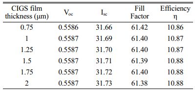
Thickness of CIGS film was speckled between 0.75 µm to 2 µm with 0.25 µm augmentation. The raise in CIGS absorber layer thickness creates great number of photon absorption which leads to improvement in efficiency. The 1.5 µm CIGS absorber layer thickness has generated an efficiency of 10.88 % and its fill factor is 61.39. And, it is observed that Voc and Jsc values are reduced as breadth of absorber coating is abridged. The reduction of absorber film breadth to ultra – thin brings rear contact much closer to depletion section [25]. The efficiency parameter variations of Voc, Jsc, FF, efficiency owing to CIGS film width in CIGS are presented in Table 4. The proficiency of CIGS as function of CIGS film thickness is depicted in Fig. 9. It is desirable to CIGS with least absorber coating breadth and predicting optimum thickness of CIGS solar cell as 1.5 µm.
Effect of i-ZnO thickness variation
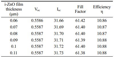
The highly resistive i-ZnO film is a crucial layer in CIGS solar cell structure for attaining high-efficiency. ZnO layer shields and protects the CdS/CIGS intersection from damage all through highly conductive current. The i-ZnO breadth in CIGS structure has been varied with 0.06 µm to 0.11 µm with 0.01 µm increment. The values of Voc, Jsc, FF, efficiency as function of i-ZnO coating breadth in CIGS is deposited in table 5. The efficiency of CIGS structure solar cell is least for 0.06 µm i-ZnO thickness with 10.86% and fill factor is 61.42. The maximum efficiency is 10.88% with a fill factor 61.4 for 0.1 µm i-ZnO thickness.
|
Fig. 2 Band chart of CIGS with band offset |
|
Fig. 3 Generation - recombination profile of CIGS. |
|
Fig. 4 (a) Current density features of CIGS in dark. (b) Current density features of CIGS under illumination. |
|
Fig. 5 The performance of CIGS on its operating temperature of CIGS. |
|
Fig. 6 Recombination Current characteristics as a function of temperature. |
|
Fig. 7 IPCE individualities as a function of temperature. |
|
Fig. 8 Performance of CdS thickness in CIGS. |
|
Fig. 9 Efficiency CIGS as function of CIGS film breadth. |
|
Table 3 Variations of Voc, Jsc, FF, efficiency due to CdS buffer layer breadth in CIGS solar cells. |
|
Table 4 Variations of Voc, Jsc, FF, efficiency as function of CIGS film breadth in CIGS performance. |
|
Table 5 Performance of Voc, Jsc, FF, efficiency by CIGS film breadth in CIGS solar cells. |
The photovoltaic behavior of CIGS solar cells was upgraded by absorber layers consisting of i-ZnO and CdS. The photo generated current density, recombination current, IPCE, band diagram, current – voltage efficiency was studied. The SCAPS program was utilized to simulate enhance the performance of CIGS. The electrical, physical material goods, thicknesses of individual layers comprising CIGS, CdS and ZnO were optimized as 1.5 µm, 0.11 µm, 0.11 µm with 290 k operating temperature. The best CIGS solar cell efficiency was observed as 11.54%. This simulated optimization of CIGS is encouraging the CIGS solar cell proficiency.
- 1. F.T. Mabvuer, F.T. Nya, and G.M.D. Kenfack, Sol. Energy 240 (2022) 193-200.
-

- 2. M. Bradha, N. Balakrishnan, A. Suvitha, T. Arumanayagam, M. Rekha, P. Vivek, P. Ajay, Ananth Steephen, Environ. Dev. Sustain. 24 (2022) 8807-8822.
-
- 3. W.Y. Parka and K.T. Lee, J. Ceram. Process. Res. 22[5] (2021) 584-589.
-
- 4. G.-L. Chiu, T. Subburaj, S. Som, C.Y. Ou, and C.-H. Lu, J. Ceram. Process. Res. 18[10] (2017) 754-759.
- 5. B. Madhavan, N. Balakrishnan, B. Pillai, and A. Steephen, J. Mater. Sci.: Mater. Electron. 32 (2021) 23066-23080.
-
- 6. S. Azizifar, M. Imanieh, S. Hassanhosseini, and F. Bahadori-Jahromi, Opt. Quant. Electron. 52[12] (2020) 514.
-
- 7. P. Murugakoothan, S. Ananth, P. Vivek, and T. Arumanayagam, J. Nano Electron. Phys. 6[1] (2014) 01003.
- 8. K. Sobayel, M. Shahinuzzaman, N. Amin, M.R. Karim, M.A. Dar, R. Gul, M.A. Alghoul, K. Sopian, A.K.M. Hasan, Md. Akhtaruzzaman, Sol. Energy 207 (2020) 479-485.
-
- 9. J. Li, K. Liu, Q. Sun, Z. Wang, and H. Wu, J. Ceram. Process. Res. 21[2] (2020) 226-232.
-
- 10. B. Madhavan, A. Suvitha, A. Steephen, and B. Pillai, J. Alloys Compd. 915 (2022) 165370.
-
- 11. Y. Zhao, S. Yuan, Q. Chang, Z. Zhou, D. Kou, W. Zhou, Y. Qi, S. Wu, Adv. Funct. Mater. (2020) 2007928.
-
- 12. H. Heriche, Z. Rouabah, and N. Bouarissa, Int. J. Hydrog. Energy 42[15] (2017) 9524-9532.
-
- 13. M. Mostefaoui, H. Mazari, S. Khelifi, A. Bouraiou, and R. Dabou, Energy Procedia 74 (2015) 736-744.
-
- 14. T. Minemoto and M. Murata, Sol. Energy Mater Sol. Cells 133 (2015) 8-14.
-
- 15. W.-Y. Parka and K.-T. Lee, J. Ceram. Process. Res. 23[2] (2022) 199-207.
-
- 16. H. Movla, Optik 125[1] (2014) 67-70.
-
- 17. M. Burgelman, J. Verschraegen, S. Degrave, and P. Nollet, Prog. Photovolt: Res. Appl. (2004) 143-153.
-
- 18. T. Garmim, N. Benaissa, A. Rmili, L. Soussi, R. Anoua, Z.E. Jouad, A. Louardi, H. Erguig, B. Hartiti, M. Monkade, Eur. Phys. J. Appl. Phys. 97 (2022) 12.
-
- 19. K. Orgassa, H. W. Schock, and J. H. Werner, Thin Solid Films. 431-432 (2003) 387-391.
-
- 20. T.S. Lopes, J.M.V. Cunha, S. Bose, J.R.S. Barbosa, J. Borme, O. Donzel-Gargand, C. Rocha, R. Silva, A. Hultqvist, W.-C. Chen, A.G. Silva, M. Edoff, P.A. Fernandes, P.M.P. Salomé, IEEE J. Photovolt. 9[5] (2019) 1421-1427.
-
- 21. B. Bissig, R. Carron, L. Greuter, S. Nishiwaki, E. Avancini, C. Andres, T. Feurer, S. Buecheler, A.N. Tiwari, Prog. Photovolt. Res. Appl. 26[11] (2018) 894-900.
-
- 22. S. H. Kima, D. Y. Lee, and Y.-J. Oh, J. Ceram. Process. Res. 21[1] (2020) 42-49.
-
- 23. T. Schneider and R. Scheer, 36th European Photovoltaic Solar Energy Conference and Exhibition (EU-PVSEC), (2019) 684-688.
- 24. H. Li, C. Xie, Y. Liao, Y. Liu, Z. Zou, and J. Wu, J. Alloys Compd. 569 (2013) 88-94.
-
- 25. P. Chelvanathan, M. I. Hossain, and N. Amin, Curr. Appl. Phys. 10 (2010) 5387-5391.
-
 This Article
-
2022; 23(6): 878-883
Published on Dec 31, 2022
- 10.36410/jcpr.2022.23.6.878
- Received on Jun 27, 2022
- Revised on Jul 19, 2022
- Accepted on Jul 21, 2022
Services
- Abstract
introduction
2. cigs structure, simulation
results and discussions
conclusion
- References
- Full Text PDF
Shared
Correspondence to
- Branesh M. Pillai
-
Center for Biomedical and Robotics Technology, Faculty of Engineering, Mahidol University, Thailand
Tel : +66-2-889-2138 Ext 6446 Fax: +66-2-441-9500 - E-mail: branesh.mad@mahidol.ac.th
Clean-Energy Research Institute(CRI), Hanyang University, 222, Wangsimni-ro, Seongdong-gu, Seoul, 04763, Korea
E-mail: jcpr@hanyang.ac.kr