


- Study on grain growth and conduction mechanism of spinel nickel ferrite ceramics
Baogang Liu*, Min Tang, Xiang Wei and Hongjuan Li
School of Energy and Electromechanical Engineering, Hunan University of Humanities, Science and Technology, Loudi 417000, China
This article is an open access article distributed under the terms of the Creative Commons Attribution Non-Commercial License (http://creativecommons.org/licenses/by-nc/4.0) which permits unrestricted non-commercial use, distribution, and reproduction in any medium, provided the original work is properly cited.
The important base of its application performance can be constituted by combining microstructure with electrical conductivity of spinel nickel ferrite ceramics. In this study, nickel ferrite ceramic powders were prepared by a high temperature solid-phase reaction and ceramic blocks were prepared by molding and sintering technology. X-ray diffraction, scanning electron microscopy, conductivity measurement and X-ray photoelectron spectrometry were employed for analyzing the phase composition, microstructure, electrical conductivity, and valence states of Fe ions. The grain growth mode and conduction mechanism of nickel ferrite ceramics were also discussed. Hexagonal growth spirals and growth hillocks were observed on each crystal plane of nickel ferrite single crystals. The growth of nickel ferrite crystals takes place by a spiral dislocation growth mechanism, indicating that the more Fe2+ ion formed in the sites of octahedral B of NiFe2O4 ceramics, the better the electrical conductivity of this ceramic materials
Keywords: Ceramics, Nickel ferrite, Grain growth, Conduction mechanism
Spinel ferrites, which serve as materials of commercial importance, are attracting years of concentration. Among various spinel ferrites, nickel ferrite is one of the most attractive materials due to its potential applications and interesting physics. Besides, they have been extensively applied in diverse fields such as data storage [1], catalysts [2], ferrofluids [3], gas sensors [4], magnetic drug delivery [5], antenna material [6] and microwave absorbers [7].
The fundamental understanding of grain growth mode and conduction mechanism of nickel ferrite is of great importance to their applications. In view of this, even after so many years, researchers still show great interest in the grain growth mode and conduction mechanism of nickel ferrite prepared by different techniques. Wang et al. prepared NiFe2O4 nanoparticles based on differential mean grain sizes by employing a sol-gel auto-combustion method. The disclosure grain growth mechanism oriented with NiFe2O4 nanoparticles aimed to follow an Ostwald ripening model and grain boundary diffusion model [8]. Šutka et al. applied sol–gel auto combustion for the synthesis of nickel ferrites of p-type with n-type conductivity in virtue of taking control of the relative nickel-iron amounts. In the meanwhile, DC resistivity measurements of room temperature appeared. The grain size did not lead to dramatic changes in resistivity that p-type nickel ferrite is featured by since the resistivity decreased through four-order magnitude in n-type nickel ferrite [9]. Chavan and other researchers provided the preparation of magnesium - doped nickel ferrite nanoparticles based on auto combustion approach. Moreover, research on the conduction mechanism of ferrites was conducted in virtue of DC resistivity in regards to temperature. According to the attained values of activation energy, the hopping made by small polarons was in charge of the conduction of electrons within nickel ferrite nanoparticles [10]. Nevertheless, to the best of our knowledge, concerning the studies of grain growth mode, up to the present, no detailed discussion has been made on the effect of the amount of Fe2+ ion on DC electrical conductivity of nickel ferrite.
In the present study, preparations on samples of NiFe2O4 were implemented on the condition of 1300 ℃ through solid state reaction. Researches were made on the grain growth mode and the effect exerted by the Fe2+ ion amounts in octahedral sites upon DC electrical conductivity of nickel ferrite, respectively. Moreover, the above-mentioned experiments were expected to provide information for understanding physical properties of spinel nickel ferrite.
Synthesis was made on samples of NiFe2O4 through solid state reaction. NiO (99%, Jinchuan, China) of high purity and Fe2O3 (99%, Qidong, China) with high purity were adopted for functioning the duty of raw materials with ball-milled in the distilled water and ZrO2 milling media, which lasted 3 hours. Additionally, 12-hour drought on the condition of 90 oC. Then, calcinations were made on the condition of 1200 oC, which lasted 6 hours in air. Subsequently, the compacts on the calcined powders were made in a uniaxial way on the condition of 50 MPa for the purpose of forming cylindrical blocks (around the diameter of 20 mm and the thickness of 40 mm). Afterwards, the sintering was made on the condition of 1300 oC, which lasted 6 hours in air and nitrogen atmospheres separately. Next, 0.2 degrees Celsius every minute was the condition of the fired samples and the following cooling in order to avoid cracking due to thermal shock.
With X-ray diffraction, examination was made on the phrases existing the samples (Rigaku D-max/2550VB+, Tokyo, Japan) on the condition of 40 KV and 250 mA based on Cu-Kα radiation. Using scanning electron microscopy, investigations on the microstructure were conducted (JEOL JSM-6360LV, Tokyo, Japan). The valence states of Fe ions were investigated by X-ray photoelectron spectroscopy (VG Multilab 2000, Thermo Electron Corporation, USA). Measurement on DC electrical conductivities was implemented at normal temperature by employing the probe approach of four points.
X-ray Diffraction Analysis
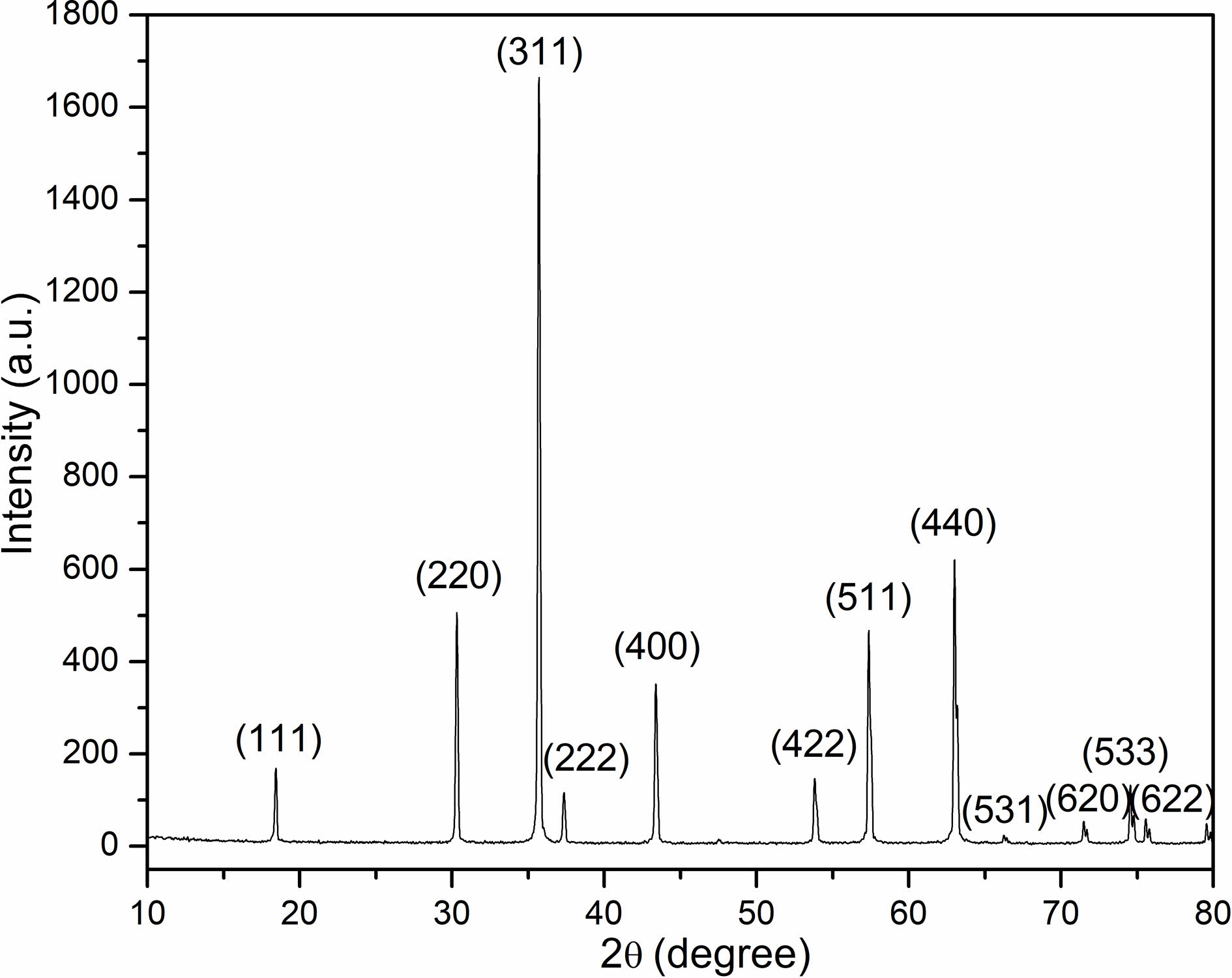
Fig. 1 illustrates the X-ray diffraction pattern in which NiFe2O4 powders calcined are characterized by at 1200 ℃ for 6 hours in air. The samples revealed polycrystalline phases situated by a typical cubic spinel structure without any signature of secondary phase. Moreover, the result stemmed out of X-ray diffraction conformed to the JCPDS Card (No. 54-0964). Calculation on the lattice constant was conducted through performing the analysis on the XRD pattern. The lattice constant was 8.342 Å, which was almost in consistence with the results reported in the literature [11-13].
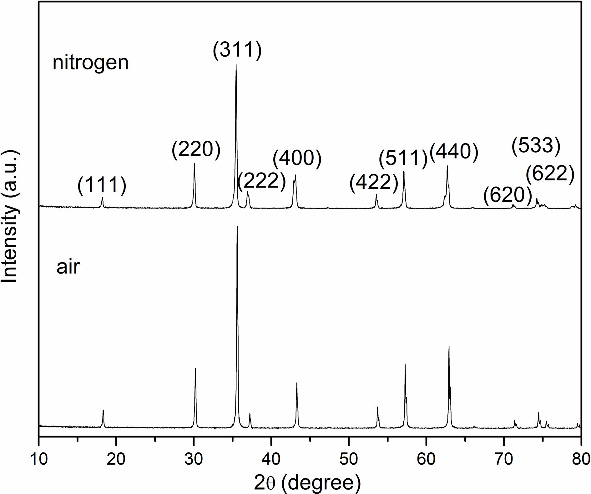
Fig. 2 shows the X-ray diffraction patterns of the samples sintered in air and nitrogen atmospheres, separately. The two samples expressed polycrystalline phases presenting a representative cubic spinel structure, indicating that there exists no phase transition during the sintering process.
Distinct grain growth phenomena
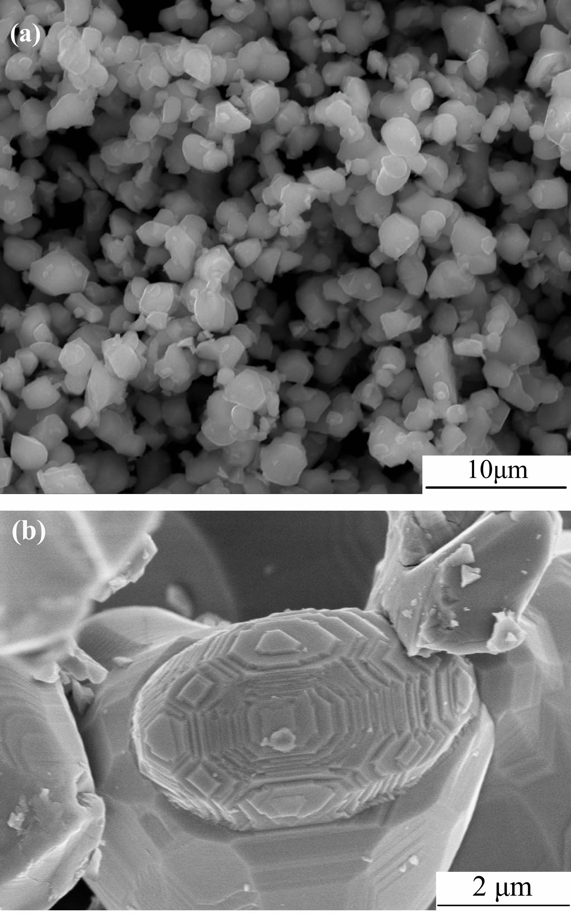
Fig. 3a demonstrates the scanning electron micrograph of NiFe2O4 particles calcined on the in-air condition of 1200 ℃ for 6 hours. Those ferrite particles featured by an average 1.5 um grain size displayed a uniform nature and some agglomeration level.
Fig. 3b expresses the scanning electron micrograph that a single-crystal nickel ferrite is featured. Hexagonal growth spirals and growth hillocks were observed on each crystal plane of nickel ferrite single crystals. It also marked the first announced instance where direct visual evidence of grain growth has been obtained on the individual crystal plane of nickel ferrite single crystals prepared by solid state reaction. Crystal growth is frequently dominated by the presence of screw dislocations on the crystal surfaces. Burton, Cabrera and Frank were the introducers of those classical models structured by the evolved vicinal surface [14]. Based on the observation of the kink sites at the facial steps, in this place, exchanges occur among the adatom layer on not only the terraces but also the solid phase. An exposed edge will be shaped wherever a screw dislocation ends up with a crystal face. During the period of growth, it will be of persistence by developing in the form of a ‘Growth Spiral’ which is oriented with dislocation. Initially, these growing spirals made a least number of turns. Then, they formed hexagonal shapes through the crystal-based hexagonal outline. The above obtained results provide convincing evidence that the growth of nickel ferrite crystals takes place by a spiral dislocation growth mechanism.
Conduction mechanism
Electrical conductivity can reflect the transporting capability which ion and electron are characterized by in a certain material [15]. Nickel ferrite ceramics serve as transition metal oxide semiconductors featuring the spinel structure and they boast low-mobility materials. It is considered that the above-mentioned transport properties could be derived out of charge transfer among those octahedral cations which was realized through the hopping made by localized d electrons. Furthermore, the electrical conductivity in ferrites could be expounded in the name of the Verwey-de Boer mechanism where electron exchanges among the ions of the same element existing within the valence state [16]. These ions exist in a random distribution over crystallographically equivalent lattice sites. Nickel ferrite, the electronic hopping occurring among Fe2+ and Fe3+ ions at octahedral sites, boasts one of the major systems allowing electrical transport [17], which could be interpreted with the electron exchanging processes as follows:

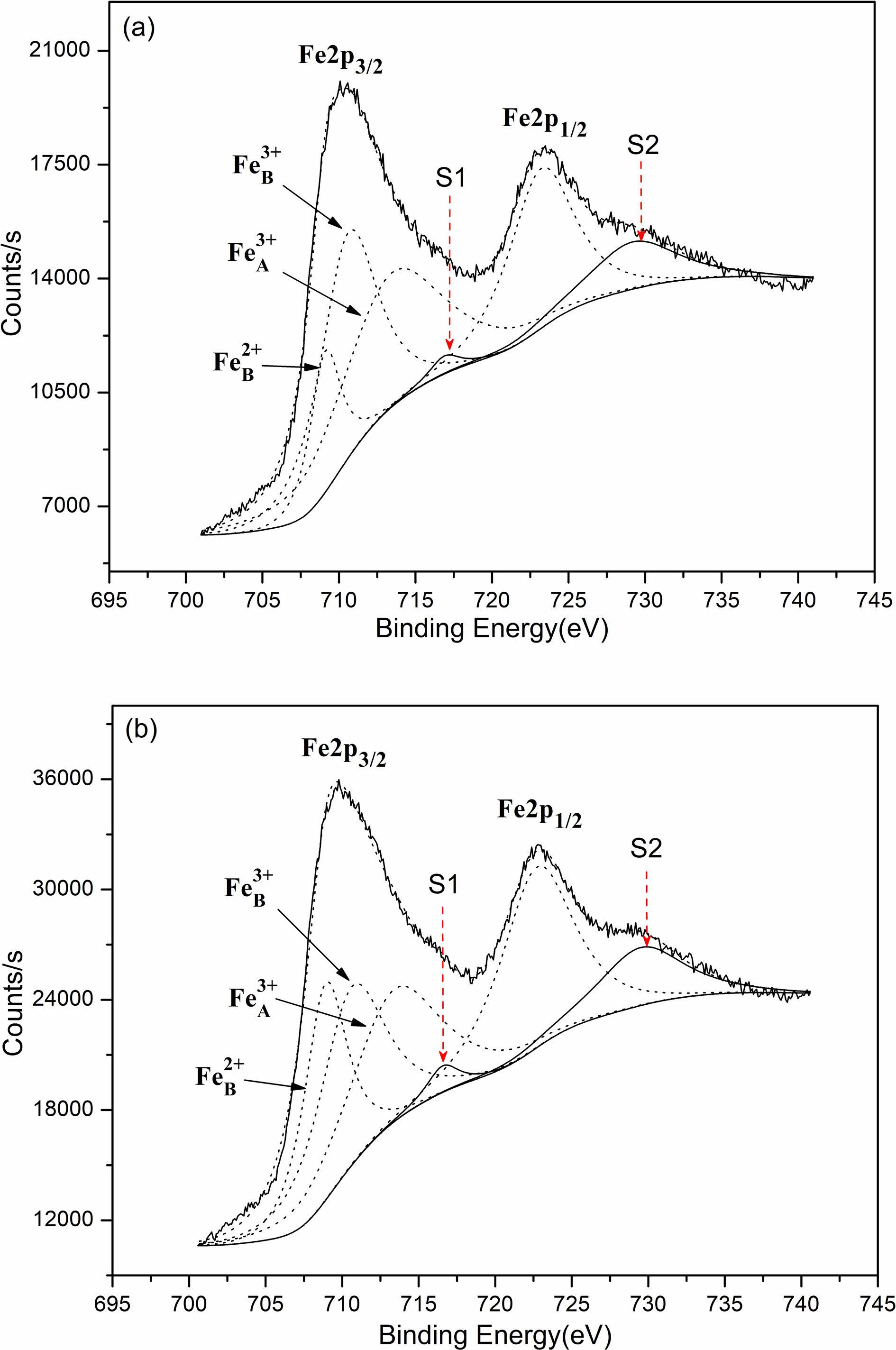
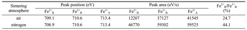
Based on the four-point probe approach, measurement was conducted to the direct current conductivities in which the samples are featured by at normal temperature. According to the results, the direct current conductivities that the samples were sintered in air were 4.11×10⁻³ S/cm, and 5.48×10⁻¹ S/cm, representing the value of the samples sintered in nitrogen. Obviously, the direct current conductivities which the samples sintered in nitrogen are featured by expressing a dramatic enhancement compared with that in-air sintered. These electrical conductivities embraced the difference from the oxygen partial pressure on the condition of sintering. Our experiment contains the synthesis of the whole nickel ferrite powders oriented with well-prepared samples in air. Initially, before sintering the above samples, the oxygen ion vacancy’s concentration in those powders presented the value in equilibrium with air. As a result, as the samples pressing in cylindrical blocks went into the atmosphere of in-air sinter and nitrogen, the gas phase was where the oxygen ions aimed to massively transfer with these oxygen molecules. Considering the much lower oxygen partial pressure on the nitrogen atmosphere compared with the in-air pressure, some lattice oxygen would be released out of the oxides as the samples were sintered in nitrogen atmosphere for forming the oxygen vacancy. Therefore, lower valence was the result of some portion of Fe3+ ions (Fe3+ → Fe2+) for maintaining the charge neutrality of lattice. These formed Fe2+ ions were strongly inclined to gain the location of the octahedral B-site [18]. The enhancing Fe2+ ion concentration located in the octahedral sites contributed to the enhancement of those electrons’ hopping rate, thus producing a more powerful electrical conductivity. By contrast, the concentration of oxygen ion vacancy featured by the in-air samples sintered represented the equal value to air. To further confirm the validity of our analysis, in virtue of X-ray photoelectron spectroscopy, examination was conducted on the Fe ions’ valence states and the Fe2+ ion concentration that the octahedral B-sites harbored. Fig. 4 demonstrate the XPS spectra of the samples sintered in air and nitrogen. Tabulation and calculation were made to the relative values in Table 1. It can be found that both Fe3+ ion and Fe2+ ion present in the two samples. The atomic rate of Fe2+B/Fe3+B for the samples sintered in nitrogen atmosphere had a dramatic enhancement when compared with in-air samples. Thus, it can be concluded that the more the Fe2+ ion amounts which was formed in the octahedral B sites of NiFe2O4 ceramics, the better the electrical conductivity of this ceramic materials.
|
Fig. 1 X-ray diffractogram of NiFe2O4 powders calcined at 1200 ℃ for 6 hours in air. |
|
Fig. 2 X-ray diffractogram of NiFe2O4 samples sintered at 1300 ℃. |
|
Fig. 3 SEM images of NiFe2O4 powders calcined at 1200 ℃ for 6 hours at different multiples: (a) ×10000; (b) ×25000. |
|
Fig. 4 XPS spectra of the samples sintered at 1300 oC: (a) sintered in air; (b) sintered in nitrogen; Fe3+A tetrahedral A-site; Fe3+B octahedral B-site; Fe2+B octahedral B-site; S1 and S2 satellite peaks. |
|
Table 1 Relative values of Fe2p peaks for NiFe2O4 samples sintered in air and nitrogen at 1300 oC. |
To conclude, nickel ferrite ceramic powders were prepared by a high temperature solid-phase reaction and ceramic blocks were prepared by molding and sintering technology. Hexagonal growth spirals and growth hillocks prove that the growth of nickel ferrite crystals takes place by a spiral dislocation growth mechanism. It indicates that the more the amount of Fe2+ ion formed at octahedral B sites of NiFe2O4 ceramics, the better the electrical conductivity of this ceramic materials.
The current work was in the support of the Scientific Research Fund of Hunan Provincial Education Department (18C0878) and the Hunan Provincial Natural Science Foundation of China (2020JJ6094).
- 1. V. Kumari, K. Dey, S. Giri, A. Bhaumik, RSC. Adv. 6 (2016) 45701.
-

- 2. H. Jian, Y. Song, A. Riisager, Catal. Sci. Technol. 8 (2018) 790.
-
- 3. P.B. Kharat, S.D. More, S.B. Somvanshi, K.M. Jadhav, J. Mater. Sci: Mater. Electron. 30 (2019) 6564.
-
- 4. J. Niresh, N. Archana, S. Neelakrishnan, V.M. Sivakumar, D.S. Dharun, J. Ceram. Process. Res. 21 (2020) 343.
-
- 5. K.S. Joshy, R. Augustine, A. Mayeen, A. Susan M, A. Hasan, S. Thomas, H. Chi, New. J. Chem. 44 (2020) 18162.
-
- 6. I. Silva, A.G. Assuno, J. Oliveira, J. Guerra, M. Sousa, Microw. Opt. Technol. Lett. 62 (2020) 2895.
-
- 7. S. Pawar, M. Gandi, I. Arief, B. Krause, P. Pötschke, S. Bose, Chemistry. Select. 2 (2017) 5984.
-
- 8. Y. Wang, L. Li, Y. Zhang, X. Chen, S. Fang, G. Li, J. Phys. Chem. C 121 (2017) 19467.
-
- 9. A. Šutka, R. Pärna, T. Käämbre, V. Kisand, Physica B 456 (2015) 232.
-
- 10. P. Chavan, L. R. Naik, Phys. Status Solidi A 214 (2017) 1700077.
-
- 11. S. Debnath, R. Das, J. Alloys Compd. 852 (2021) 156884.
-
- 12. M. Khan, S. Bisen, J. Shukla, A. Mishra, P. Sharma, J. Supercond. Nov. Magn. 34 (2021) 763.
-
- 13. T. Vigneswaria, P. Rajib, J. Ceram. Process. Res. 17 (2016) 999.
- 14. W.K. Burton, N. Cabrera, F.C. Frank, Phil. Trans. Roy. Soc. London, Ser. A 243 (1951) 299.
-
- 15. B. Liu, K. Zhou, Z. Li, D. Zhang, L. Zhang, Mater. Res. Bull. 45 (2010) 1668.
-
- 16. L.G. Van Uitert, J. Chem. Phys. 23 (1955) 1883.
-
- 17. V. Baco-Carles, I. Pasquet, V, Laurent, A. Gabriel, P. Tailhades, Solid. State. Sci. 11 (2009) 1503.
-
- 18. M. Bhagavantha Reddy, V. Devender Reddy, P. Venugopal Reddy, Mod. Phys. Lett. B 8 (1994) 959.
-
 This Article
-
2022; 23(6): 770-773
Published on Dec 31, 2022
- 10.36410/jcpr.2022.23.6.770
- Received on Sep 1, 2021
- Revised on Nov 11, 2021
- Accepted on Nov 27, 2021
Services
- Abstract
introduction
experimental
results and discussion
conclusion
- Acknowledgements
- References
- Full Text PDF
Shared
Correspondence to
- Baogang Liu
-
School of Energy and Electromechanical Engineering, Hunan University of Humanities, Science and Technology, Loudi 417000, China
Tel : +86-738-8326910 Fax: +86-738-8326910 - E-mail: liudd2016@126.com
Clean-Energy Research Institute(CRI), Hanyang University, 222, Wangsimni-ro, Seongdong-gu, Seoul, 04763, Korea
E-mail: jcpr@hanyang.ac.kr