


- Microstructure and piezoelectric properties of (K,Na)NbO3 ceramics prepared by pre-annealed sintering for piezoelectric energy harvester
J.H. Kim†, K.W. Chae and C.I. Cheon*
Department of Materials Science & Engineering, Hoseo University, Asan 31499 Korea
†Current Address: Dept. of Functional Ceramics, Ceramic Materials Division, Korea Institute of Materials ScienceThis article is an open access article distributed under the terms of the Creative Commons Attribution Non-Commercial License (http://creativecommons.org/licenses/by-nc/4.0) which permits unrestricted non-commercial use, distribution, and reproduction in any medium, provided the original work is properly cited.
The pre-annealed sintering method was attempted to obtain (K,Na)NbO3 ceramics with a homogeneous microstructure without abnormal grain growth for multi-layered piezoelectric energy harvester application. The CuO and Na2CO3-doped (K,Na)NbO3 ceramics by normal sintering at temperatures above 900 oC displayed excellent piezoelectric properties but showed an inhomogeneous microstructure due to an abnormal grain growth. Meanwhile, the ceramics sintered at temperatures of 880-900 oC showed a homogeneous microstructure and poor piezoelectric properties. The grain growth was influenced by a grain shape in a normal sintering. The sample that were sintered at temperatures of 880-900 oC with round-edged grains showed a normal grain growth, whereas samples sintered at temperatures above 900 oC with faceted grains exhibited abnormal grain growth. The specimen sintered at 940 oC for 3 hours after pre-annealing at 900 oC for 6 hours showed a homogeneous microstructure and excellent piezoelectric properties which are suitable for multi-layered piezoelectric energy harvesting applications. An electromechanical coupling factor (kp), piezoelectric strain constant (d33), and mechanical quality factor (Qm) were 0.431, 143 pC/N, and 737, respectively and the figure of merits for a piezoelectric energy harvester in the resonance (kp2∙Qm) and off-resonance conditions (d33∙g33) were 137 and 7.5 pm2/N in the sample prepared by a pre-annealed sintering
Keywords: Piezoelectric, Pre-annealed sintering, (K,Na)NbO3, Energy harvester
A piezoelectric energy harvester (PEH), which generates electricity from ambient mechanical vibrations, has attracted attention in recent years due to their potential use in wireless self-powered sensor nodes [1-7]. The performance of a PEH is dependent on the energy conversion efficiency of a piezoelectric ceramic and the structure of the PEH [4-11]. The generated energy (U) by a PEH is represented by the equation:
where dij, gij, F, and A are the piezoelectric strain constant, the piezoelectric voltage constant, the applied force, and the area of the energy harvester, respectively [4-9]. The product of dij and gij has been defined to be the figure of merit (FOM) of a piezoelectric material under off-resonance conditions. In the resonance condition, the energy conversion efficiency is proportional to kij2·Qm, where kij and Qm are an electromechanical coupling factor and a mechanical quality factor, respectively [8-11]. Previously, it has been reported that PEHs made from multi-layered ceramics have large currents and low voltages than PEHs with a single-layered ceramic [12]. However, since expensive noble metals are used as internal electrodes in the multi-layered PEH structure, the piezoelectric ceramics are demanded to be co-fired at a low temperature with internal metal electrodes to minimize the amount of noble metal [13].
Due to the environmental and health concerns associated with lead-based piezoelectrics, considerable efforts have been focused on the development of lead-free piezoelectric ceramics [14-20]. (K,Na)NbO3 (KNN)-based solid solution ceramics are promising candidates that have shown outstanding piezoelectric properties and are expected to be commercialized in various piezoelectric applications [14-18]. KNN-based ceramics doped with CuO have been reported to be sintered at low temperatures below 950 oC and have a high figure of merit for PEH [21, 22]. However, CuO-doped KNN-based ceramics have showed abnormally-grown large grains and are difficult to be applied for the PEH composed of tens of micrometer-thick ceramic multilayer layers [21, 22].
A two-step sintering has been tried to suppress the abnormal grain growth (AGG) in piezoelectric ceramics [23-25]. The two-step sintering process first involves rapidly heating to a temperature higher than a normal sintering, followed by a second step of cooling down to low temperature to obtain a dense sample. This two-step approach has previously been demonstrated to successfully constrict grain growth and create a dense ceramic with nanometer-sized grains [26]. Two-step sintering has resulted in a homogeneous microstructure without AGG in KNN-based and (Bi,Na)TiO3-based ceramics by reducing the rate of AGG [23-25]. A pre-annealed sintering method, in which a sample was annealed for several hours at a temperature below AGG starts and then sintered at higher temperature, has also been explored to suppress AGG in KNN-based ceramics [27]. However, this pre-annealed sintering method was only partially effective in inhibiting AGG in KNN-based ceramics [27]. These previous results suggest that the processing conditions such as pre-annealing temperature, holding time and heating rate must be properly controlled to completely inhibit AGG in KNN.
In this work, we attempt to utilize the pre-annealed sintering method to obtain KNN ceramics with a homogeneous microstructure without AGG for multi-layered PEH application. We adopted the modified KNN composition, (K0.453Na0.482Li0.065)(Nb0.99Ta0.01)O3 which has been reported to have high FOMs for PEH [9]. 0.5 mole % CuO and 1 mole % Na2CO3 was doped to the sample for low temperature sintering. The samples were pre-annealed and sintered at temperatures below 950 oC. As a means of comparison, we also prepared samples with the normal sintering method. We then characterized the phases, microstructures and electrical properties in the samples prepared by the pre-annealed sintering and the normal sintering.
We prepare the samples by a conventional ceramic process from the following starting materials: K2CO3, Na2CO3, Li2CO3, Nb2O5, and Ta2O5 powders with purities over 99%. These raw materials were ball-milled with ethyl alcohol and zirconia balls for 24 hours. The resulting slurry was dried and calcined at 800 oC for 4 hours. 1 mole % Na2CO3 and 0.5 mole % CuO was included in the powder as a low-temperature sintering aid and then mixed again for 24 hours by ball milling. One mole % Na2CO3 was expected to compensate for the sodium evaporation during the heat treatment. We also added 0.5 wt. % polyvinyl butyral during the ball-milling as a binder. Disk-shaped compacts were formed by pressing and the binder was burned out at 600 oC for 2 hours. The samples were pre-annealed at 900 oC for 6 hours and then sintered at 940 oC for 3 hours in the pre-annealed sintering method. The samples prepared with the normal sintering method were sintered at 880-940 oC for 3 hours in a single step. The samples were heated to the pre-annealing temperature or the sintering temperature at a ramp rate of 5 oC/min. and were cooled in a furnace in both pre-annealed and normal sintering processes. To perform the electrical measurements, we printed silver paste on the sample and then fired at 800 oC for 10 minutes.
We utilized X-ray diffraction (XRD, XRD-6100, Shimadzu) and scanning electron microscope (SEM, SEC, SNE-4500E) to examine the crystal structures and microstructures of the samples. The densities after sintering were measured by Archimedes’ principle. We perform poling (dipole alignment) by applying a DC electric field of 4-5 KV/mm for 30 minutes at 100 oC in silicon oil. An impedance analyzer (HP4294A) was used to measure the frequency dependence of the capacitances, impedances and phases of the samples. The piezoelectric constant was measured using a d33 meter (YE2730A, APC International Ltd.). Impedance data from a resonance method were used to calculate the electromechanical coupling factor (kp) and mechanical quality factor (Qm) of the samples [22].
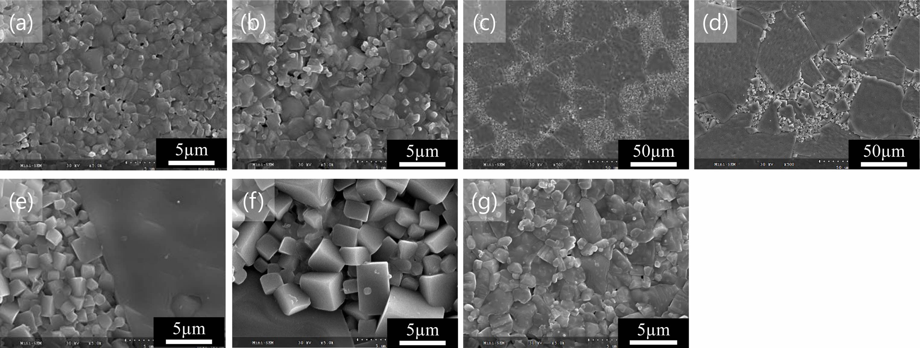
Fig. 1 shows microstructures of the KNN ceramics prepared with the normal sintering method at (a) 880 oC, (b) 900 oC, (c, e) 920 oC and (d, f) 940 oC for three hours, and the sample prepared with the pre-annealed sintering method (g) that was pre-annealed at 900 oC for 6 hours and then sintered at 940 oC for 3 hours. The samples prepared by the normal sintering method at temperature of 880-900 oC (Fig. 1a,b) display round-edged small grains with a diameter of a few micrometers. However, the samples prepared at sintering temperature of 920-940 oC (Fig. 1c-f) show heterogeneous microstructures with small and large grains, where the size of the large grains (tens of micrometers) is approximately ten times larger than the small matrix grains (a few micrometers). A similar bimodal grain size distribution was reported to result from abnormal grain growth (AGG) [28-32]. Similar AGG was reported in KNN ceramics with excess Na2O or CuO-doped KNN samples and was promoted by liquid phase formation at sintering temperatures above 900 oC [21, 22, 28, 29]. Whereas large abnormal grains were observed in the samples that were prepared by the normal sintering method at temperatures above 900 oC, they are not present in the SEM images of the sample pre-annealed at 900 oC and sintered 940 oC as shown in Fig. 1(g). The sample prepared by the pre-annealed sintering has comparable micrometer-sized grains and grain morphology to the sample sintered at 900 oC by the normal sintering method.
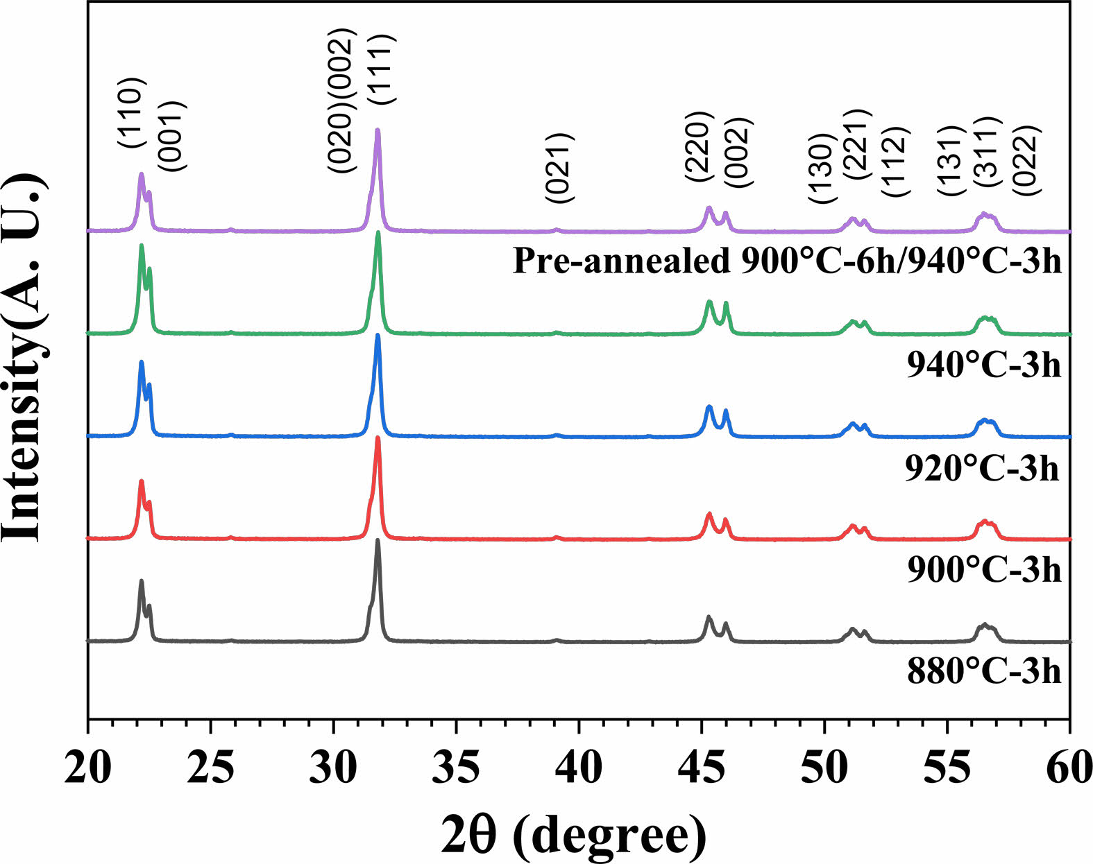
Fig. 2 displays X-ray diffraction patterns of the samples sintered at 880-940 oC for three hours by a normal sintering and the sample prepared by pre-annealed sintering at 900 oC for 6 hours and 940 oC for 3 hours. All samples display a perovskite single phase with an orthorhombic crystal structure. The X-ray diffraction patterns suggest there are no impurities present in any of the sample and we do not observe any distinct difference in crystal structure among any of the samples. This result suggests that the microstructural differences observed in the SEM images of the KNN samples are not due to differences in the crystal structures of the samples.
The equilibrium grain shape has been reported to govern the grain growth behavior; faceted grains grow abnormally, but rounded grains grow normally [33-37]. Since round grains with rough interfaces have many nucleation sites, they grow normally by diffusion-controlled growth [33-37]. However, faceted grains with an atomically ordered interfaces grow by a two-dimensional nucleation-controlled growth mechanism and have a critical driving force for grain growth [33-37]. As a result, faceted grains grow abnormally because grains with the small driving force cannot grow, while grains with a high driving force can grow significantly [33-37].
Fig. 1 shows that samples prepared by normal sintering at 880 oC and 900 oC (Fig. 1a, b) result in grains with rounded edges, whereas the samples sintered at temperatures above 900 oC exhibit faceted edges in both the large abnormally-grown grains and the small matrix grains. The grain shape seems to have an important role in the grain growth behavior in CuO-doped KNN materials as well. The samples with faceted grains showed an AGG while the samples with round-edged grains displayed a normal grain growth, as shown in Fig. 1. Liquid phase formation has been reported to change an interface structure and a grain shape [33, 37]. The change in the grain morphology from rounded to faceted due to the formation of a large amount of a liquid phase has been observed in Bi2O3-added (Bi,Na)TiO3-BaTiO3 ceramics [37]. Our results suggest that a significant amount of liquid phase at sintering temperatures above 900 oC results in changing the grain shape from round-edged grains to faceted grains in CuO-doped KNN ceramics. The grain shape appears to be formed at an early stage of the sintering such that the samples with faceted grains showed an AGG, while the samples with round-edged grains exhibit a normal or a pseudo-normal grain growth. However, even after sintering at 940 oC for 3 hours, the sample prepared by the pre-annealed method exhibits small round-edged grains without abnormally-grown large grains, as shown in Fig. 1(g). This result demonstrates that the pre-annealed sintering method can effectively inhibit abnormal grain growth in the KNN ceramics. The microstructure and the density of the sample prepared by the pre-annealed sintering method (pre-annealed at 900 oC for 6 hours and then sintered at 940 oC for 3 hours) were comparable to those of the sample sintered at 900 oC for 3 hours by a normal sintering, as shown in Fig. 1 and Table 1. In the sample manufactured by the pre-annealed sintering method, the liquid phase formed when sintering at 940 oC for 3 hours could not change the grain morphology and grain growth behavior since the microstructure development and the densification were almost finished in the pre-annealing step.
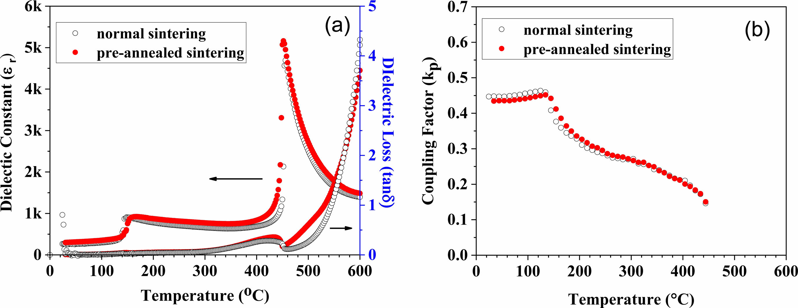
Fig. 3 shows the temperature dependence of (a) the dielectric permittivities (εr) and losses (tanδ), and (b) electromechanical coupling factors (kp) for the samples prepared by a normal sintering at 920 oC for 3 hours and the sample prepared by a pre-annealed sintering method. The sharp dielectric peaks corresponding to Curie temperatures (Tc) are observed at high temperatures around 450 oC in both samples. The pre-annealed sample showed another dielectric anomaly at a temperature around 162 oC due to a phase transition from an orthorhombic to a tetragonal structure (TO-T) which is slightly higher than that of the sample prepared by normal sintering. Fig. 3(b) shows that the kp remains at a constant value of approximately 0.44 until TO-T, monotonically decreases at temperatures above TO-T, and then drops to zero at Tc in both samples.
The piezoelectric characteristics of the samples prepared by a normal sintering and pre-annealed sintering are listed in Table 1. The samples sintered at 880 and 900 oC for 3 hours by the normal sintering method showed a small piezoelectric constant (d33), electromechanical coupling factor (kp) and mechanical quality factor (Qm) even though the sample sintered at 900 oC had a high density that is about 95% of the theoretical value. The high electric field could not be applied to the samples that were normally sintered at 880 and 900 oC for 3 hours due to low insulating resistance, which resulted in incomplete dipole alignment to the applied electric field and poor piezoelectric properties [25]. Table 1 displays a considerable improvement in the piezoelectric characteristics for the samples that were prepared by the normal sintering method at temperatures above 900 oC. It has previously been suggested that the diffusion of Cu ions from grain boundaries into the grains can lead to an enhancement in the piezoelectric characteristics of CuO-doped KNN ceramics when sintered at temperatures above 900 oC [20, 25]. The Cu ions substituting for the B site ions have been shown to result in a hardening effect that decreases the permittivity and increases Qm in KNN-based ceramics [38-40]. We find that the samples sintered above 900 oC exhibit a decreased dielectric constant and significantly increased Qm as shown in Table 1. Our results also show that the Cu substitution resulted in an enhanced kp by improving the degree of poling.
The sample prepared by a pre-annealed sintering at 900 oC for 6 hours and 940 oC for 3 hours shows outstanding piezoelectric properties; kp = 0.431, d33= 143 pC/N, and Qm = 737. These results suggest that the Cu ions diffuse from grain boundaries to grain interiors during the pre-annealed sintering procedure. Table 1 shows that the pre-annealed sample had high FOMs for PEHs in the resonance and off-resonance conditions: kp2∙Qm = 137 and d33∙g33 = 7.5 pm2/N. Notably, the piezoelectric characteristics and FOMs for PEH of the sample prepared by a pre-annealed sintering method are comparable to those of samples sintered at 920-940 oC by a normal sintering method. Furthermore, whereas the samples sintered at 920-940 oC by the normal sintering method exhibit AGG, the sample prepared by the pre-annealed sintering method exhibits a homogeneous microstructure without abnormally-grown large grains, as shown in Fig. 1. These findings suggest that pre-annealed sintering is an effective method to prepare KNN-based ceramics for multi-layered PEH applications.
|
Fig. 1 Microstructures of the samples sintered at 880 oC (a), 900 oC (b), 920 oC (c, e) and 940 oC (d, f) for three hours by a normal sintering, and the sample sintered 940 oC for 3 hours after pre-annealing at 900 oC for 6 hours (g). |
|
Fig. 2 X-ray diffraction patterns of the samples sintered at 880- 940 oC for three hours by a normal sintering and the sample sintered 940 oC for 3 hours after pre-annealing at 900 oC for 6 hours. |
|
Fig. 3 Temperature dependences of (a) dielectric permittivities (εr) and losses (tanδ), and (b) electromechanical coupling factors (kp) in the sample sintered at 920 oC for 3 hours by a normal sintering and the sample sintered 940 oC for 3 hours after pre-annealing at 900 oC for 6 hours. |
|
Table 1 Piezoelectric properties and FOMs for a piezoelectric energy harvester in KNN ceramics prepared by normal sintering and pre-annealed sintering. |
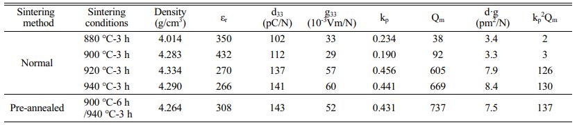
The CuO and Na2CO3-doped KNN ceramics prepared by normal sintering at temperatures above 900 oC displayed excellent piezoelectric properties but suffers from an inhomogeneous microstructure which is not adequate for multi-layered piezoelectric energy harvesting devices. The grain morphology changed from round-edged to faceted in the samples prepared by a normal sintering when the sintering temperature increased above 900 oC. The change of the grain shape led to a shift in the grain growth behavior from a normal to an abnormal grain growth. However, a sample sintered at 940 oC for 3 hours after pre-annealing at 900 oC for 6 hours showed a uniform microstructure with a few micrometer-sized grains. The microstructure of the sample prepared by a pre-annealed sintering was not changed during a sintering at 940 oC for 3 hours because a densification and microstructure development were finished at a pre-annealing step. The samples prepared by a pre-annealed sintering had excellent piezoelectric properties that were comparable to the samples prepared by normal sintering at temperatures above 900 oC: kp = 0.431, d33 = 143 pC/N, and Qm = 737. The sample prepared by a pre-annealed sintering had high FOMs for a piezoelectric energy harvester in the resonance and off-resonance conditions which were kp2∙Qm = 137 and d33∙g33 = 7.5 pm2/N.
This research was supported by the Academic Research Fund of Hoseo University in 2018 (20180360).
- 1. C. Covaci and A. Gontean, Sensors 20 (2020) 3512.
-

- 2. M. Safaei, H.A. Sodano, and S.R. Anton, Smart Mater. Struct. 28 (2019) 113001.
-
- 3. H. Liu, J. Zhong, C. Lee, S.-W. Lee, and L. Lin, Appl. Phys. Rev. 5 (2018) 041306.
-
- 4. S. Priya, H.-C. Song, Y. Zhou, R. Varghese, A. Chopra, S.-G. Kim, I. Kanno, L. Wu, D.S. Ha, J. Ryu, and R.G. Polcawich, Energy Harvesting and Systems 4[1] (2017) 3-39.
-
- 5. T. Rödig, A. Schönecker, and G. Gerlach, J. Am. Ceram. Soc. 93 (2010) 901-912.
-
- 6. S. Priya, J. Electroceram. 19 (2007) 165-182.
-
- 7. K.-S. Lee, M.-S. Chae, D.-J. Shin, S.-M. Nam, J.-H. Koh, S.-J. Jeong, K.-H. Cho, and S.W. Chang, J. Ceram. Process. Res. 13[S2] (2012) s278-s281.
- 8. I.-T. Seo, C.-H. Choi, D. Song, M.-S. Jang, B.-Y. Kim, S. Nahm, Y.-S. Kim, T.-H. Sung, and H.-C. Song, J. Am. Ceram. Soc. 96[40] (2013) 1024-28.
-
- 9. S.H. Go, D.S. Kim, S.H. Han, H.-W. Kang, H.-G. Lee, and C.I. Cheon, J. Kor. Ceram. Soc. 54 (2017) 530-534.
-
- 10. C.D. Richards, M.J. Anderson, D.F. Bahr, and R.F. Richard, J. Micromech. Microeng. 14[5] 717-21 (2004).
-
- 11. M. Umeda, D. Nakamura, and S. Ueha, Jpn. J. Appl. Phys. 35[5B] (1996) 3267-73.
-
- 12. H.-C. Song, H-C. Kim, C.-Y. Kang, H.J. Kim, S.-J. Yoon, and D.-Y. Jeong, J Electroceram. 23 (2009) 301-304.
-
- 13. S. Kawada, M. Kimura, Y. Higuchi, and H. Takagi, Appl. Phys. Express 2 (2009) 111401.
-
- 14. Y. Saito, H. Takao, T. Tani, T. Nonoyama, K. Takatori, T. Homma, T. Nagaya, and M. Nakamura, Nature 432 (2004) 84-87.
-
- 15. J.-F. Li, K. Wang, F.-Y. Zhu, L.-Q. Cheng, and F.-Z. Yao, J. Am. Ceram. Soc. 96 (2013) 3677-3696.
-
- 16. H. Wu, Y. Zhang, J. Wu, J. Wang, and S.J. Pennycook, Adv. Funct. Mater. (2019) 1902911.
-
- 17. L. Zeng, R. Benioub, and K. Itaka, J. Ceram. Process. Res. 23[1] (2022) 62-68.
-
- 18. I.-H. Im, S.-H. Lee, H.-K. Kim, D.-H. Lee, S.-H. Kim, Y.-S. Yun, Y.-K. Choi, and S.-P. Nam, J. Ceram. Process. Res. 15[1] (2014) 26-29.
- 19. J. Roedel, W. Jo, K.T.P. Seifert, E.-M. Anton, and T. Granzow, J. Am. Ceram. Soc. 92 (2009) 1153-1177.
-
- 20. J. Rödel, K.G. Webber, R. Dittmer, W. Jo, M. Kimurac, and D. Damjanovic, J. Eur. Ceram. Soc. 35 (2015) 1659-1681.
-
- 21. R. Huang, Y. Zhao, X. Zhang, Y. Zhao, R. Liu, and H. Zhou, J. Am. Ceram. Soc. 93[12] (2010) 4018-21.
-
- 22. J.H. Kim, J.S. Kim, S.H. Han, H.-W. Kang, H.-G. Lee, and C.I. Cheon, Mater. Res. Bull., 96[2] (2017) 121-25.
-
- 23. J. Fang, X. Wang, Z. Tian, C. Zhong, L. Li, and R. Zuo, J. Am. Ceram. Soc. 93 (2010) 3552-3555.
-
- 24. S.-Y. Ko and S.-J.L. Kang, J. Eur. Ceram. Soc. 36 (2016) 1159-1165.
-
- 25. J.H. Kim, D.S. Kim, S.H. Han, H-W. Kang, H.-G. Lee, J.S. Kim, and C.I. Cheon, Mater. Lett. 241 (2019) 202-205.
-
- 26. I.-W. Chen and X.-H. Wang, Nature 404 (2000) 168-171.
-
- 27. S.H. Moon, J.H. Choi, K.W. Chae, J.S. Kim, and C.I. Cheon, Ceram. Int. 39 (2013) 2431-2436.
-
- 28. M.S. Kim, D.S. Lee, E.C. Park, S.J. Jeong, and J.S. Song, J. Eur. Ceram. Soc. 27 (2007) 4121-4124.
-
- 29. M.S. Kim, S.J. Jeong, and J.S. Song, J. Am. Ceram. Soc. 90 (2007) 3338-3340.
-
- 30. S.J.L. Kang, M.G. Lee, and S.M. An, J. Am. Ceram. Soc. 92[7] (2009) 1464-1471.
-
- 31. S.-J.L. Kang, J.-H. Park, S.-Y. Ko, and H.-Y. Lee, J. Am. Ceram. Soc. 98[2] (2015) 347-360.
-
- 32. S.-J.L. Kang, S.-Y. Ko, and S.-Y. Moon, J. Ceram. Soc. Jpn. 124[4] (2016) 259-267.
-
- 33. Y.I. Jung, D.Y. Yoon, and S.-J.L. Kang, J. Mater. Res. 24 (2009) 2949-2959.
-
- 34. S.-J.L. Kang, M.G. Lee, and S.MJ. An, Am. Ceram. Soc. 92 (2009) 1464-1471.
-
- 35. S.-J.L. Kang, J.-H. Park, S.-Y. Ko, and H.-Y. Lee, J. Am. Ceram. Soc. 98[2] (2015) 347-360.
-
- 36. S.-J.L. Kang, S.-Y. Ko, and S.-Y. Moon, J. Ceram. Soc. Jpn. 124[4] (2016) 259-267.
-
- 37. S.-C. Jeon, J.G. Fisher, S.-J.L. Kang, and K.-S. Moon, Materials 13 (2020) 1344.
-
- 38. J.B. Lim, S. Zhang, J.-H. Jeon, and T.R. Shrout, J. Am. Ceram. Soc. 93[5] (2010) 1218-1220.
-
- 39. J.-J. Zhou, L.-Q. Cheng, K. Wang, X.-W. Zhang, J.-F. Li, H. Liu, and J.-Z. Fang, Ceram. Int. 40 (2014) 2927-2931.
-
- 40. H.-S. Han, J. Koruza, E.A. Patterson, J. Schultheiß, E. Erdem, W. Jo, J.-S. Lee, and J. Rödel, J. Eur. Ceram. Soc. 37 (2017) 2083-2089.
-
 This Article
-
2022; 23(5): 679-684
Published on Oct 31, 2022
- 10.36410/jcpr.2022.23.5.679
- Received on Apr 6, 2022
- Revised on May 17, 2022
- Accepted on Jun 4, 2022
Services
- Abstract
introduction
experimental
results and discussion
summary
- Acknowledgements
- References
- Full Text PDF
Shared
Correspondence to
- C.I. Cheon
-
Department of Materials Science & Engineering, Hoseo University, Asan 31499 Korea
Tel : +82-41-540-5763 Fax: +82-41-540-5768 - E-mail: cicheon@hoseo.edu
Clean-Energy Research Institute(CRI), Hanyang University, 222, Wangsimni-ro, Seongdong-gu, Seoul, 04763, Korea
E-mail: jcpr@hanyang.ac.kr