


- Resistive switching random access memory based on Sn-incorporated Cs(PbxSn1-x)Br3 perovskite thin films
Seung-Beom Cho†, Hye-Yun Seong† and Il-Kyu Park*
Department of Materials Science and Engineering, Seoul National University of Science and Technology, Seoul 01811, Korea
This article is an open access article distributed under the terms of the Creative Commons Attribution Non-Commercial License (http://creativecommons.org/licenses/by-nc/4.0) which permits unrestricted non-commercial use, distribution, and reproduction in any medium, provided the original work is properly cited.
We investigated the performance of resistive random access memory (RRAM) consisting of Sn-incorporated Cs(PbxSn1-x)Br3 thin films. The uniform Cs(PbxSn1-x)Br3 perovskite thin films with various Sn contents were formed by using the solution-based spin coating method. The structural and optical investigations showed that the Sn element was successfully incorporated into the CsPbBr3 lattice. As the Sn content increases, secondary phases like SnBr2 and CsSn2Br5 were also formed in the Cs(PbxSn1-x)Br3 perovskite thin films. RRAM device consisting of the pristine CsPbBr3 thin film showed typical RRAM switching behavior and an operating voltage of about 0.7 V. The RRAM switching behavior of the CsPbBr3 was suggested based on the migration of halide vacancies, which forms the conducting filament when the electric field is applied. As the content of the Sn element increases, the transition voltage shifted to the lower voltage side to about 0.3~0.4 V. The switching performances of the RRAM device were affected by the Sn content in the Cs(PbxSn1-x)Br3 perovskite thin films due to the formation of defects and secondary phases
Keywords: Perovskite, CsPbBr3, Lead-free, RRAM, Phase control
The growth of memory technology has been appro- aching its limit as the device scale-down technologies are developed for a few decades. As one of the solutions to this problem, the performance of non-volatile memory has been improved by changing the insulator to high-k materials or modifying the device architecture to a three-dimensional flash memory type structure. As an alternative memory device, new memories like magnetic, phase-change, and resistive random-access memory (RRAM) have been studied actively [1-5]. Among them, RRAM has achieved much attention because it exhibits a much faster access time than flash memory and low power consumption [2-7]. It usually operates at low voltages of 2~5 V or less [2-7]. In addition, because of the simple MIM (Metal-Insulator-Metal) structure, it is advantageous for high integration by making the cell area of the device much smaller, as well as reducing the production cost compared to other memory devices with a relatively simple process [2-7]. The RRAM structure mainly uses inorganic materials, such as metal oxide or chalcogenide, which are difficult to realize high flexibility and high light transmittance than conventional memories could not achieve [3-8]. In addition, to realize wearable or foldable devices, research on flexible memory structure should be developed. Recently, lead halide perovskite (LHP) and halide lead-free halides have attracted great attention for next generative semiconducting materials due to their unique optical and electrical properties, such as feasible bandgap engineering through exchanging the halogen elements, high color gamut, sharp and narrow emission peak, and large exciton energy [8-12]. Even though CsPbBr3 thin film or nanostructures have been applicated as active materials for photovoltaic and light-emitting diodes, few have been reported about the perovskite-based RRAM devices [8-14]. The CsPbBr3-based LHP can be an excellent candidate for RRAM devices because it possesses polarity depending on the polymorphs. At room temperature, it has an orthorhombic structure and has anti-polarization properties. Therefore, it is expected to exhibit a hysteresis property according to the polarity, and the structure changes into orthorhombic, tetragonal, and cubic according to the conditions. However, the Pb element in the ceramic structure is a toxic heavy metal, which has been classified as a carcinogen as well as environmental pollution and harmful to the human body [15,16]. Therefore, Pb-free or Pb-less containing LHP materials for the switching medium of RRAM should be developed for commercial applications. In this study, we fabricated the Sn-based Pb-less containing Cs(PbxSn1-x)Br3 thin films and adopted them into the switching medium of the RRAM device.
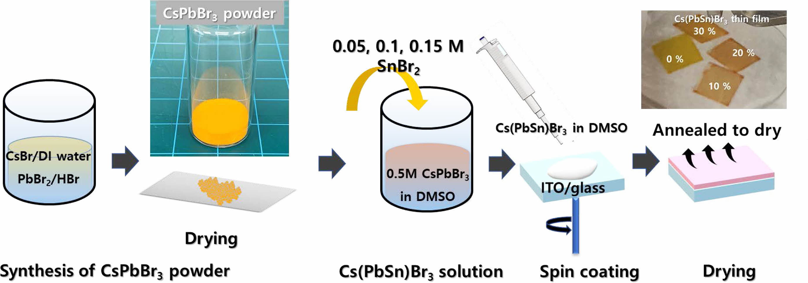
Fabrication
Sn-incorporated Cs(PbxSn1-x)Br3
thin films were fabricated based on a spin-coating method as shown schematically
in Fig. 1. The source solution for the thin
films was prepared by dissolving the synthesized Sn-incorporated CsPbBr3
sources. The pristine CsPbBr3 powder was synthesized by
precipitating the PbBr2 solution using a CsBr solution. At first,
PbBr2 (10 mM) and CsBr (10 mM) were dissolved in the mixed solution
of hydrobromic acid (8 mL) and DI water (3 mL). The prepared CsBr solution was
mixed with the PbBr2 solution. The resultant precipitate
was an orange-colored powder as shown in Fig. 1. This precipitate
was purified by washing with ethanol and annealed at the temperature of 60 °C
for 12 hrs. To make a source solution, CsPbBr3 powder (0.5 M) was
dissolved in dimethyl sulfoxide (DMSO). Various amount of SnBr2 with
mole concentration of 0.05 (10 mol%), 0.1 (20 mol%), and 0.15 M (30 mol%) were
added into the CsPbBr3 precursor solution. The pristine and
Sn-incorporated Cs(PbxSn1-x)Br3 thin films
were fabricated by spin coating the prepared solution onto the already-cleaned
indium tin oxide (ITO) glass substrate. The Sn-incorporated Cs(PbxSn1-x)Br3
solutions were spin-coated onto the ITO/glass substrate at 2,000 rpm for 60
sec. All process was performed in a glove box. The color of the Sn-incorporated
CsPbBr3 thin film changed from light to dark brown color with
increasing the Sn molar content as shown in Fig. 1. This would be due to the
reduction in energy bandgap with increasing the incorporated Sn content into
the CsPbBr3 thin films. The remnant solvent was removed by annealing
at 80 °C for 15 min. After thin film formation, the 100 nm-thick-aluminum
electrode was evaporated through a shadow mask with a diameter of 500 mm at a pressure of 10−6
Torr to form the Al/Cs(PbxSn1-x)Br3/ITO
structure of the RRAM device.
Characterization
The surface topography of the Sn-incorporated Cs(PbxSn1-x)Br3
thin films was measured by using a field-emission
scanning electron microscope (FE-SEM). The crystalline
quality was investigated by X-ray diffraction (XRD) by measuring a
Cu Kα radiation source with λ=0.154 nm. The optical properties of the Sn-incorporated
Cs(PbxSn1-x)Br3 thin films were studied
by UV-visible absorption spectroscopy (Agilent 8453). The
photoluminescence (PL) spectrum was measured by using a spectrophotometer (MAYA
2000 PRO) with a 405 nm laser. The current-voltage (I-V)
measurements were performed using a source meter (Keithley 2450).
|
Fig. 1 The processing steps for fabricating Sn-incorporated Cs(PbxSn1-x)Br3 thin films using the solution-based spin coating method. |
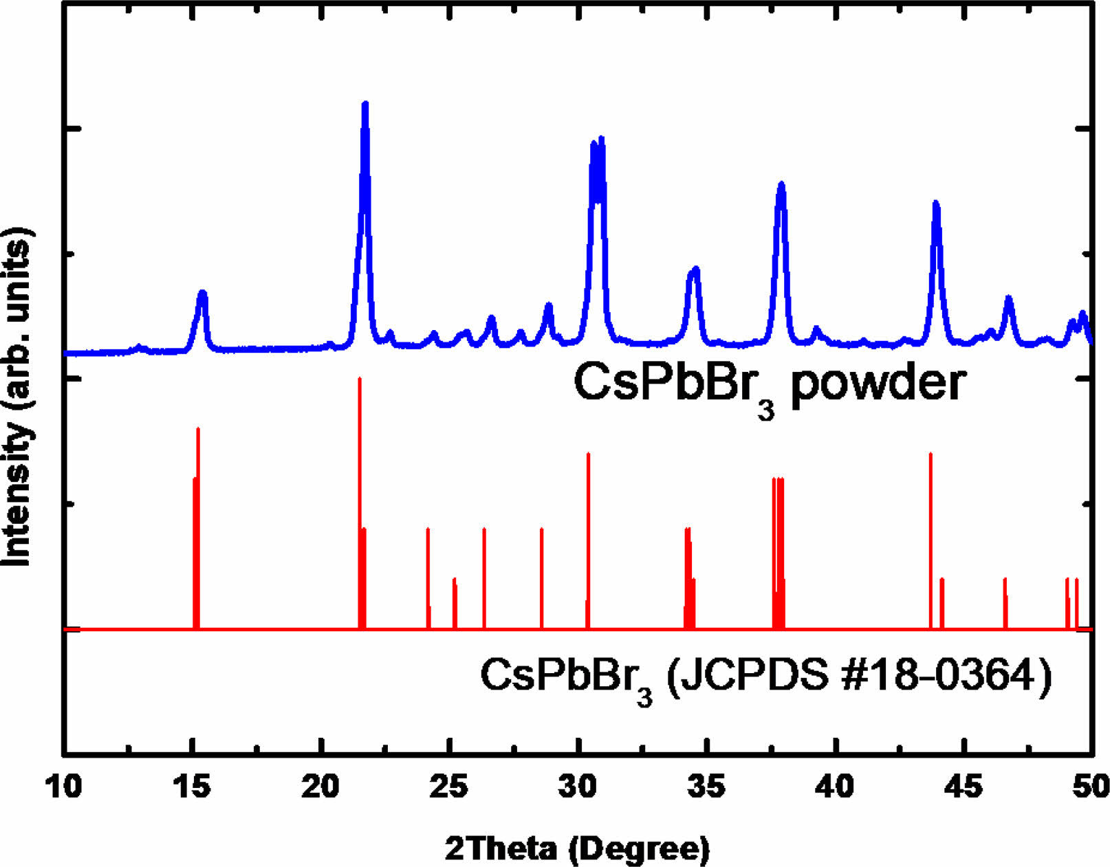
To confirm the crystalline structure of the CsPbBr3 source powders, XRD was measured for the pristine powder before dissolving in the DMSO solvent (Fig. 2). The XRD result shows major patterning peaks at 15.09o, 21.30o, 30.58o, 34.18o, 37.67o, and 43.57o, which are assigned to the (100), (110), (200), (201), (211), and (202) planes of the crystal structure of the CsPbBr3 with lattice parameter a = b = c = 5.82 Å (#18-0364) [17]. The XRD results also showed that there are no secondary phases of Cs4PbBr6 or CsPb2Br5.
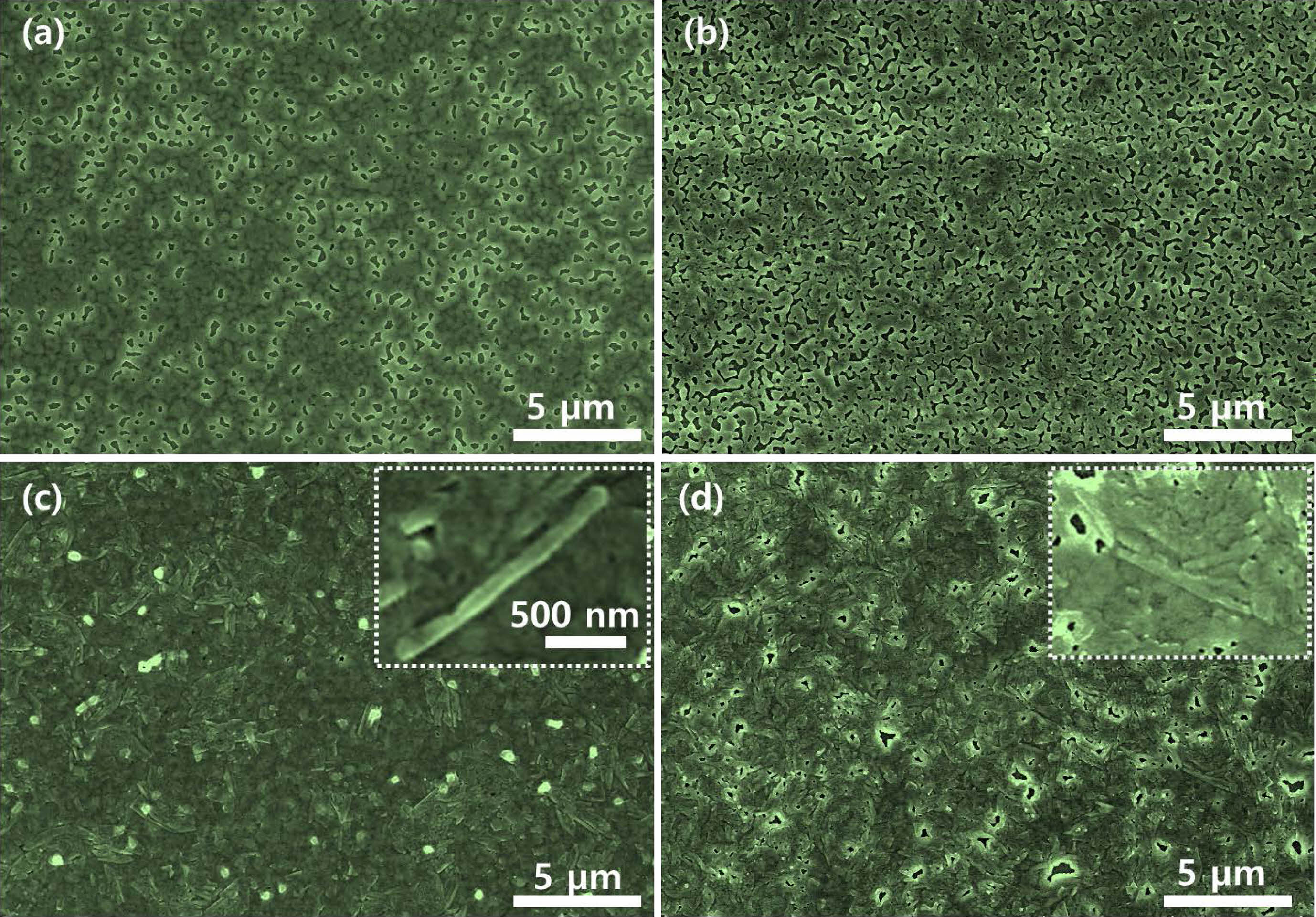
Fig. 3 presents FE-SEM images of the Sn-incorporated Cs(PbxSn1-x)Br3 thin film surfaces with the variation of the Sn content. The pristine and Sn-incorporated Cs(PbxSn1-x)Br3 thin films were formed uniformly whole of the surface. However, as the Sn content increases, the pinhole defect increases gradually. Especially, needle-like crystallites were found as the Sn content increases above 20 mol% (Figs. 3(c) and (d)). These needle-like crystals are corresponding to the excessively precipitated SnBr2, which is similar to that observed on the CsSnI3 film surface when the content of SnI2 is too high [18, 19]. The increased uncovered pinhole-like regions would be due to the crystallization of the excess SnBr2, which impedes the growth of high surface coverage thin films.
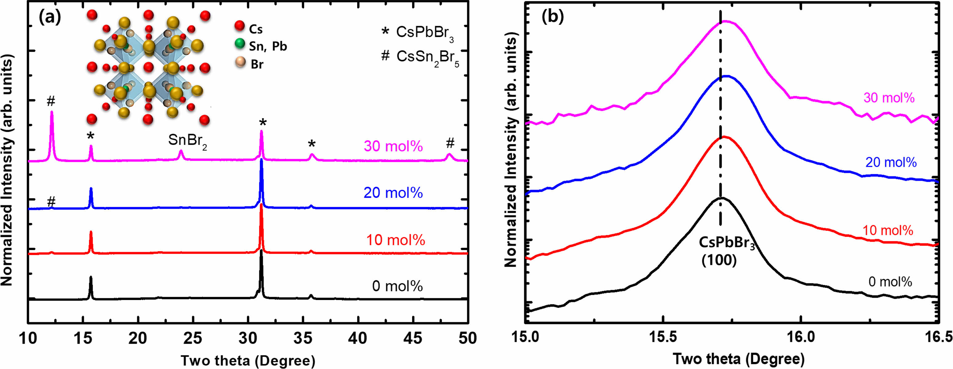
The effect of Sn incorporation on the structural evolution of the Cs(PbxSn1-x)Br3 thin films was investigated by using XRD measurement as shown in Fig. 4. The diffraction data were matched well with the cubic phase (JCPDS No. 18-0346) [17]. The pure CsPbBr3 and Sn-incorporated Cs(PbxSn1-x)Br3 thin films showed the same cubic crystal structure. At the same time, the secondary phase of tetragonal CsSn2Br5 starts to appear as the SnBr2 molar content is larger than 10 %. In addition, as the molar content of SnBr2 is more than 30%, the CsSn2Br5 phase dominates and the SnBr2 starts to be precipitated without being incorporated as shown in Fig. 4(a). To confirm the incorporation of the Sn element into the Cs(PbxSn1-x)Br3 lattice, the (100) diffraction peak was investigated as shown in Fig. 4(b). The (100) diffraction peak shifted to a larger angle side as the SnBr2 molar content increased. This would be due to lattice shrinkage with increasing the incorporated Sn content by substituting the Pb sites in the CsPbBr3 crystal lattice. The ionic radius of Sn2+ is 118 pm, which is smaller compared to that of Pb2+ (119 pm) [20]. The lattice parameter of the Sn-incorporated Cs(PbxSn1-x)Br3 crystal structure would reduce with increasing the SnBr2 molar content. Therefore, the XRD results indicate that the Sn elements are incorporated into the CsPbBr3 lattice and simultaneously form secondary phases such as SnBr2 and CsSn2Br5.
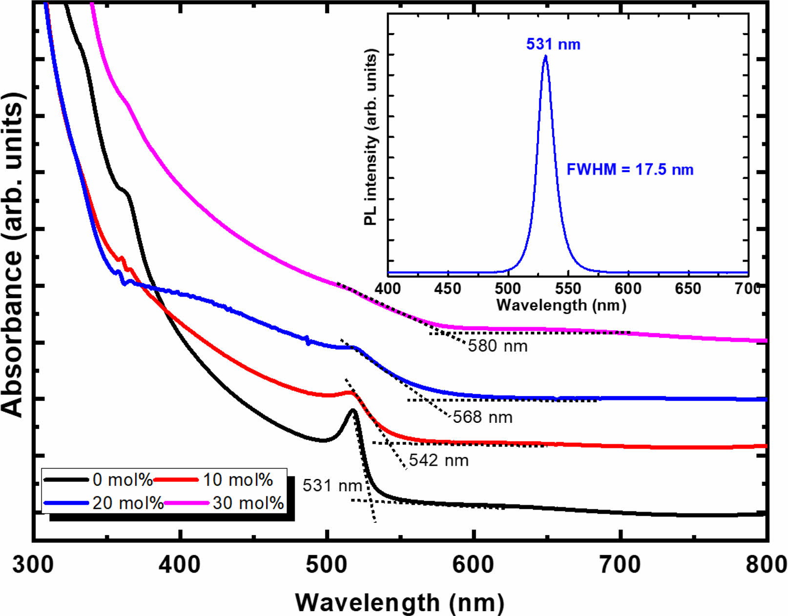
Fig. 5 shows the UV-visible absorption spectra and PL spectrum of the Cs(PbxSn1-x)Br3 thin films with various SnBr2 content. The feature of the spectra changes with increasing the SnBr2 content. The pure CsPbBr3 exhibited a clear absorption edge and an exciton-related sharp absorption peak at 517 nm. This feature is similar to the previous results for the CsPbBr3 thin films formed by the solution process [13, 14, 21]. The pristine thin film also showed symmetric emission peaks centered at 531 nm with a very narrow full-width at a half-maximum (FWHM) value of 17.5 nm. The UV-visible absorption and emission spectra indicate that the pristine CsPbBr3 thin film exhibits uniform and excellent crystalline quality. As the SnBr2 content increases from 0 to 30 mol%, the absorption edge shifts to the longer wavelength side from 531 to 580 nm. The bandgap energies of CsPbBr3 and CsSnBr3 are 2.42 and 1.382 eV, respectively [19, 20]. Therefore, the red-shift of the absorption edge of the Sn-incorporated Cs(PbxSn1-x)Br3 thin films indicates that the Sn was incorporated successfully by substituting the Pb site. The sharp exciton absorption peaks reduce gradually as the SnBr2 content exceeds 20 mol%. This would be due to the gradual degradation of the crystalline quality of the Cs(PbxSn1-x)Br3 structure with the incorporation of the Sn element by a large difference in ionic radius compared to the Pb element.
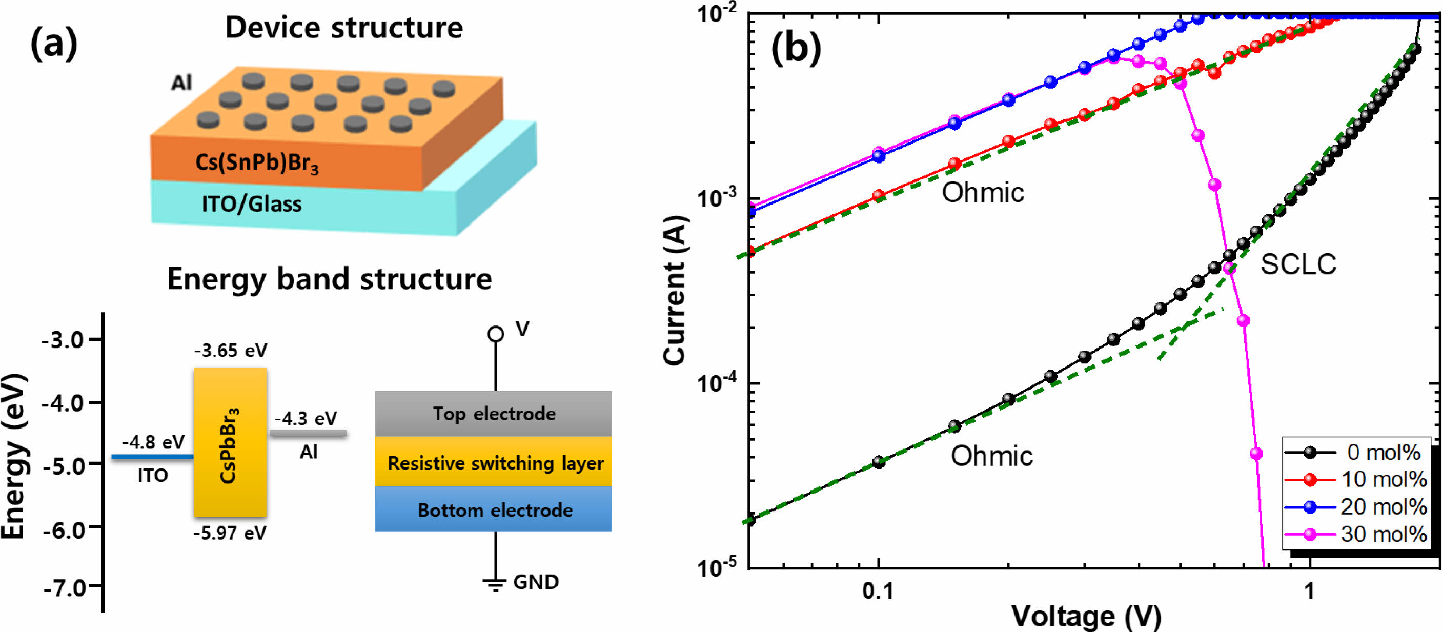
Based on the Sn-incorporated Cs(PbxSn1-x)Br3 thin films, we fabricated all-inorganic perovskite nonvolatile RRAM devices. The schematic of the Al/Cs(PbxSn1-x)Br3/ITO device structure and corresponding energy band diagram are shown in Fig. 6(a). To study the transport properties of electrical charge carriers of the devices, the log I-log V curves were analyzed. Figs. 6(b) shows the double logarithmic scale I-V curves of the Sn-incorporated CsPbBr3 thin film-based memory cells in the sweep-voltage region from 0 to 2 V. The current flows easier through the Cs(PbxSn1-x)Br3 perovskite layer as the Sn content increases due to a reduction in bandgap energy of the Cs(PbxSn1-x)Br3 perovskite alloys and increased formations of defects and secondary phases with increasing the Sn content. In the case of pristine CsPbBr3 thin film, the I-V curve clearly shows that the conduction through the active layer was dominated by Ohmic transport at the low voltage region and space charge limited current (SCLC) at the higher voltage region, respectively. At the low voltage region, the results showed linear dependence and the slope was approximately 1. This implies that the carrier transport is dominated by the Ohmic mechanism. In the high voltage region, the current increases more drastically as the electrical bias increases. This is consistent with the Child’s square law dominated by the SCLC mechanism (I~V 2) [4-8]. The threshold voltage for the transition from Ohmic to SCLC conduction regions indicates the change of conduction mechanisms from the trap-unoccupied to the trap-occupied region by traps. At this voltage, the conducting filaments are generated in the CsPbBr3 thin films between the top and bottom electrodes. The conduction mechanism dominated by the trap-controlled SCLC originated from the defect states existing in the CsPbBr3 film, which are formed during solution methods at low temperatures. In the case of Sn-incorporated Cs(PbxSn1-x)Br3 film, only Ohmic conduction is observed. The 30 mol% sample shows the short circuit during device operation due to the generation of the conduction channel through the CsPbBr3 layer. In addition, current flows more easily as the Sn content increases. This would be due to the generation of more conductive CsSn2Br5 phases in the CsPbBr3 films with increasing the SnBr2 molar content as shown in XRD results.
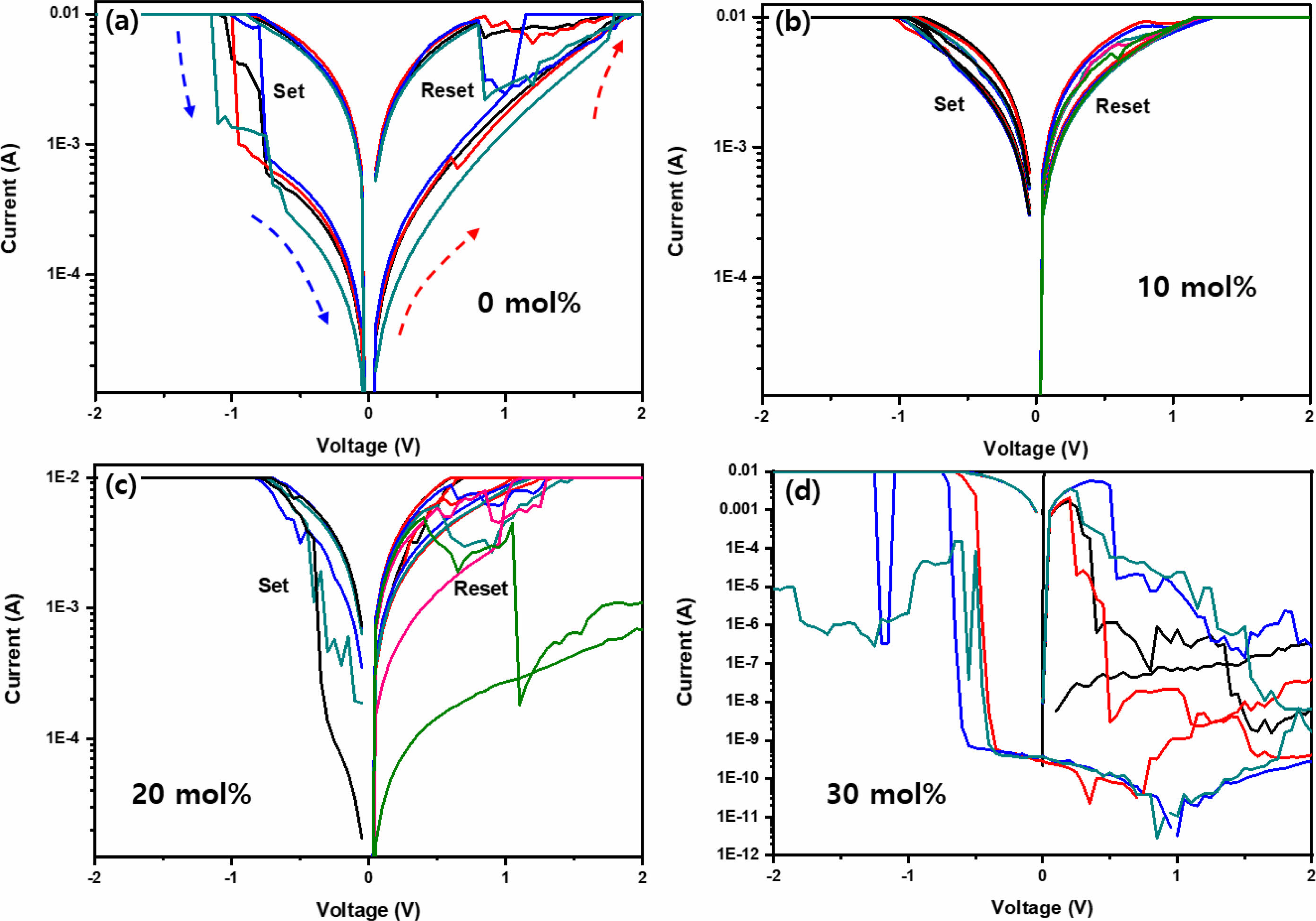
The resistive switching effect was investigated based on the Sn-incorporated Cs(PbxSn1-x)Br3 thin films with varying SnBr2 molar content. In general, an electroforming process is required to operate the RRAM devices. In this work, the electroforming process was performed by applying the bias from 0 to 3.0 V. The compliance current was limited to 10 mA to avoid device breakdown and excessive Joule heating. Fig. 7(a) shows the typical I-V characteristics of the memory devices consisting of Al/pristine CsPbBr3/ITO structure on a semilogarithmic scale. Clear hysteresis curves exhibiting both “Set” and “Reset” behaviors appear clearly for the pristine CsPbBr3 thin film. To study the hysteresis behavior, the origin of the conduction channel in the CsPbBr3 thin film should be identified. Generally, metal halide perovskite thin films contain various defects, such as grain boundaries, interstitials, substitutions, anti-site substitutions, and vacancies [24, 25]. Among them, vacancies have been known as the main defect because they have low formation energy. In this case, vacancy-mediated diffusion is a common process in the CsPbBr3 perovskite structure [24, 25]. Among the vacancies, the formation of halide vacancy (V•Br) is the most favorable because it has the lowest activation energy of formation [24]. RRAM operation behavior in the perovskite materials occurs by the migration of defects and trapping of electrical charges under the applied bias. Vacancy defects create shallow levels in the energy band and migrate by hopping between the nearest neighboring atoms [25]. The CsPbBr3 perovskite consists of corner-sharing negatively charged PbBr6 octahedra and positively charged Cs+ at the center as shown in the inset of Fig. 4(a). In the structure, halide ion (Br-) moves feasibly along an octahedral edge because it can be the shortest conducting channel. At the thermal equilibrium state without applying the bias, these defects are distributed randomly in the Cs(PbxSn1-x)Br3 perovskite layer. Under the applied bias, the positively charged bromine vacancies (V•Br) would drift to gather near the negatively biased electrode, which forms positively charged vacancy filaments that can be formed and connect electrically between the Al and ITO electrodes. This is referred to as the Set process. The vacancies become neutral by recombination with electrons. As the applied bias increases, the trap levels formed by defects are filled, and electrons conduct by hopping between the traps. The conduction path is reduced as the electron de-trapping occurs during the Reset process. In the case of pristine CsPbBr3, the Reset occurs at about 0.8 V, and the Set behavior occurs at about -1 V, where the current dramatically increased. At this bias, the high resistance state (HRS) was triggered by the low resistance state (LRS). After the forming process by applying a bias, the CsPbBr3 film showed the transition from the HRS to the LRS. By applying the positive and negative bias sweeping to the LRS film, at around 0.8~0.9 V (Reset voltage), the current level was reduced significantly. The Cs(PbxSn1-x)Br3 thin films are switched to the HRS. As the Sn content increases, the transition voltage, where Set and Reset behaviors occur, shifts to the lower voltage side to about 0.3~0.4 V. In addition, the device operation becomes unstable. The Set process is formed due to the filament formation and the bias to occur this process decreases from -1 to -0.5 V as the molar content of SnBr2 increases from 0 to 20 mol%. In addition, as the content of Sn content increases more up to 30 mol%, the device does not operate anymore. As the SnBr2 molar content increases, the CsSn2Br5 and SnBr2 phases are dominated as shown in XRD results. In this case, a large number of vacancies would be formed and facilitates the current flow even at low bias. The formation of filament acts as conducting paths by lowering the resistance required for ions to move even at low applied bias. Therefore, it is possible to predict the result that the voltage caused by the Set/Reset of the RRAM is lowered due to the formation of vacancies. By considering the UV-visible absorption analysis results, it could be estimated that the bandgap energy of the perovskite decreased according to the Sn content due to the occurrence of a redshift in the graph. As a result, as the bandgap decreases, the current can flow more easily through the conductive device. Therefore, the Sn incorporation into the CsPbBr3 alloy can modulate the RRAM performances by inducing defect formation and secondary phases.
|
Fig. 2 XRD patterns of synthesized pristine CsPbBr3 powders to prepare the precursor solution for the spin coating process. |
|
Fig. 3 FE-SEM images of Sn-incorporated Cs(PbxSn1-x)Br3 surfaces with variation of SnBr2 content. (a) pure CsPbBr3 (0 mol%), (b) 0.05 M (10 mol%), (c) 0.1 M (20 mol%), and (d) 0.15 M (30 mol%). |
|
Fig. 4 (a) XRD patterns of Sn-incorporated Cs(PbxSn1-x)Br3 thin films with changing the SnBr2 content. The inset shows the crystal structure of Cs(PbxSn1-x)Br3. (b) Variation of (100) diffraction peak position with a variation of molar content of SnBr2. |
|
Fig. 5 UV-vis absorption spectra of Sn-incorporated Cs(PbxSn1-x)Br3 thin films with a variation of molar content of SnBr2. The inset shows the PL spectra of the pristine CsPbBr3 thin film. |
|
Fig. 6 (a) Schematic of device structure and electron energy band diagram of the Cs(PbxSn1-x)Br3 thin film-based RRAM device. (b) The log-log scale I-V curves of the RRAM with the Cs(PbxSn1-x)Br3 thin films with various Sn content. |
|
Fig. 7 Semilogarithmic scale I-V curves of the RRAM devices based on the Cs(PbxSn1-x)Br3 thin films with various Sn content. (a) pristine CsPbBr3 (0 mol%), (b) 0.05 M (10 mol%), (c) 0.1 M (20 mol%), and (d) 0.15 M (30 mol%). |
In summary, we fabricated and investigated the performance of RRAM devices based on Sn-incorporated Cs(PbxSn1-x)Br3 thin films with various Sn content. The uniform Sn-incorporated Cs(PbxSn1-x)Br3 perovskite thin films were deposited by using the solution-based spin coating method. The structural investigations showed that the Sn element was successfully incorporated into the CsPbBr3 lattice and simultaneously formed secondary phases, such as SnBr2 and CsSn2Br5. The fabricated RRAM device fabricated by using pristine CsPbBr3 thin film exhibited reproducible and reliable resistive switching behavior and showed a low operation voltage of about 0.7 V. The resistive switching behavior was explained based on the migration of halide vacancies, which formed the conducting filament under the electric field. As the Sn element is incorporated, the transition voltage, where Set and Reset behaviors occur, shifted to the lower voltage side to about 0.3~0.4 V. The device performance was affected by the formation of vacancy defects and secondary phases as the Sn element is incorporated into the Cs(PbxSn1-x)Br3 thin film. Therefore, the formation of unexpected vacancy and secondary phases should be considered to fabricate the lead-free perovskite thin film-based switching devices.
This study was supported by the Research program funded by the Seoultech (Seoul National University of Science & Technology)
- 1. S. Jung, H. Lee, S. Myung, H. Kim, S.K. Yoon, S.W. Kwon, Y. Ju, M. Kim, W. Yi, S. Han, B. Kwon, B. Seo, K. Lee, G.-H. Koh, K. Lee, Y. Song, C. Choi, D. Ham, and S. J. Kim, Nature 601 (2022) 211-216.
-

- 2. D.B. Strukov, G.S. Snider, D.R. Stewart, and R.S. Williams, Nature 453 (2008) 80-83.
-
- 3. R. Waser, R. Dittmann, G. Staikov, and K. Szot, Adv. Mater. 21 (2009) 2632-2663.
-
- 4. J.W. Seo, J.W. Park, and K.S. Lim, Appl. Phys. Lett. 93 (2008) 223505.
-
- 5. R. Waser and M. Aono, Nat. Mater. 6 (2007) 833-840.
-
- 6. S.Y. Lee, S.H. Cho, H.K. Kim, J.H. Oh, H.J. Kim, S.K. Hong, J.S. Roh, and D.J. Choi, J. Ceram. Process. Res. 10 (2009) 433-436.
- 7. H. Cho, C.W. Jeon, B.D. On, I.K. Park, S. Choi, J. Jang, and G. Wang, Adv. Mater. Interfaces 8 (2021) 2001990.
-
- 8. S.B. An, J.H. Jeong, and D.J. Choi, J. Ceram. Process. Res. 16 (2015) 560-564.
-
- 9. H. Kim, J.S. Han, S.G. Kim, S.Y. Kim, and H.W. Jang, J. Mater. Chem. C 7 (2019) 5226-5234.
-
- 10. J.S. Han, Q. VanLe, and J. Choi, ACS Appl. Mater. Interfaces 11 (2019) 8155.
-
- 11. T. Tsuruoka, K. Terabe, T. Hasegawa, and M. Aono, Nanotechnology 21 (2010) 425205.
-
- 12. T.T. Mau and K.H. Kim, J. Ceram. Process. Res. 13 (2012) 301-304.
- 13. S.B. Cho, J.W. Jung, Y.S. Kim, C.H. Cho, and I.K. Park, CrystEngComm 23 (2021) 2746-2755.
-
- 14. J.B. Cho, S.B. Cho, and I.K. Park, J. All. Compd. 891 (2022) 161996.
-
- 15. J.G. Fisher, K.H. Lee, and W.J. Moon, J. Ceram. Process. Res. 21 (2020) 5-13.
-
- 16. V.Q. Nguyen, H.S. Han, H.B. Lee, J.I. Yoon, K.K. Ahn, and J.S. Lee, J. Ceram. Process. Res. 13 (2012) 282-285.
- 17. G. Hu, W. Qin, M. Liu, X. Ren, X. Wu, L. Yang, and S. Yin, J. Mater. Chem. C 7 (2019) 4733-4739.
-
- 18. P. Mauersberger and F. Huber, Acta Crystallogr., Sect. B 36 (1980) 683-684.
-
- 19. Z. Shum, J. Chen, C. Qureshi, J. Yu, W. Wang, N. Pfenninger, J. Vockic, J. Midgley, and J. Kenney, Appl. Phys. Lett. 96 (2010) 221903.
-
- 20. Y. Zhou and Y. Zhao, Energy Environ. Sci. 12 (2019) 1495-1511.
-
- 21. L. Zhang, X. Yang, Q. Jiang, P. Wang, Z. Yin, X. Zhang, H. Tan, Y. Yang, M. Wei, B.R. Sutherland, E.H. Sargent, and J. You, Nat. Commun. 8 (2017) 15640.
-
- 22. M. Roknuzzaman, K.K. Ostrikov, H. Wang, A. Du, and T. Tesfamichael, Sci. Rep. 7 (2017) 14025.
-
- 23. D.E. Scaife, P.F. Weller, and W.G. Fisher, J. Solid State Chem. 9 (1974) 308-314.
-
- 24. C. Eames, J.M. Frost, P.R. Barnes, B.C. O’regan, A. Walsh, and M.S. Islam, Nat. Commun. 6 (2015) 7497.
-
- 25. C. Gu and J.S. Lee, ACS Nano 10 (2016) 5413-5418.
-
 This Article
-
2022; 23(5): 672-678
Published on Oct 31, 2022
- 10.36410/jcpr.2022.23.5.672
- Received on Mar 20, 2022
- Revised on May 31, 2022
- Accepted on Jun 4, 2022
Services
- Abstract
introduction
experimental procedure
results and discussion
conclusions
- Acknowledgements
- References
- Full Text PDF
Shared
Correspondence to
- Il-Kyu Park
-
Department of Materials Science and Engineering, Seoul National University of Science and Technology, Seoul 01811, Korea
Tel : +82-2-970-6349 Fax: +82-2-973-6657 - E-mail: pik@seoultech.ac.kr
Clean-Energy Research Institute(CRI), Hanyang University, 222, Wangsimni-ro, Seongdong-gu, Seoul, 04763, Korea
E-mail: jcpr@hanyang.ac.kr