


- Structural and electrical properties of K(Ta0.62Nb0.38)O3/BiFeO3 multilayer films for electrocaloric devices
Jeong-Eun Lima,†, Myung-Gyu Leea,b,†, Byeong-Jun Parka, Sam-Haeng Leea,b, Joo-Seok Parkb, Young-Gon Kimc and Sung-Gap Leea,*
aDept. of Materials Engineering and Convergence Technology, RIGET, Gyeongsang National University, Jinju 52828, Korea
bBusiness Support Division, Korea Institute of Ceramic Engineering and Technology, Jinju 52851, Korea
cDept. of Electronics, Chosun College of Science and Technology, Gwangju 61453, KoreaThis article is an open access article distributed under the terms of the Creative Commons Attribution Non-Commercial License (http://creativecommons.org/licenses/by-nc/4.0) which permits unrestricted non-commercial use, distribution, and reproduction in any medium, provided the original work is properly cited.
KTN/BFO multilayer films were manufactured using the spin-coating method on Pt/Ti/SiO2/Si substrate with KTN(62/38) and BFO metal alkoxide solutions. The mean thickness of the multilayer films was about 420-450 nm. A rough interfacial layer was observed at the interface between the lower substrate and the film when sintered at 650oC. Dense microstructures without pores inside of the films were shown via TEM analysis, and an interface between the KTN and BFO layers was clearly observed. The Curie temperature was about 16oC. Dielectric constant and dielectric loss were 1380 and 0.384 at 20oC, respectively. Coercive field of the 2-layer and 6-layer films were 72.6 and 80.4 kV/cm at room temperature, respectively. ΔT and EC coefficient of the 6-layer films sintered at 630oC were 1.96oC and 0.13×10⁻⁶ oCmV-1, respectively
Keywords: Multilayer films, BFO, KTN, Electrocaloric effect, Sol-gel method
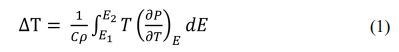
The Electrocaloric (EC) effect is a phenomenon where a reversible temperature change occurs due to a change in the arrangement of dipole moments when an electric field is applied to ferroelectric materials. In 2006, a giant electrocaloric (ΔT) effect was observed in PZT films [1]. Therefore, many studies were conducted through the changing of different variables, such as phase transition temperature control, improvement of ferroelectric properties, lead-free ceramics, etc. and applying them to electrocaloric devices at near room temperature [2]. ΔT is calculated from Eq. (1) from the Maxwell relations [1], where C and ρ are the specific heat and density, respectively.
Bismuth ferrite (BiFeO3, BFO), having rhombohedral unit cells at room temperature, has a distorted perovskite structure. Multiferroic BFO, which simultaneously exhibits ferroelectric, antiferromagnetic, and ferroelastic properties, has a high Curie temperature of 850 oC and large remanent polarization of about 100 μC/cm2 [3]. BFO ceramics have potential application in ferroelectric random access memory (FeRAM), spintronic devices, and sensors [4]. However, BFO has serious leakage current and low breakdown voltage properties.
Potassium tantalate niobates (KTa1-xNbxO3, KTN) are a compatible solid solution compound of KTaO3 and KNbO3; the crystal structure and Curie temperature can be modulated by controlling the Ta/Nb composition ratio. Ferroelectric KTN has high dielectric constant, low loss tangent, and large electro-optic effect. KTN has been studied for application to tunable microwaves and electro-optic devices [5, 6]. In recent years, researches on the pyroelectric and EC effects have also been actively conducted. [7, 8]. However, KTN has a disadvantage in that it is difficult to fabricate a specimen of stoichiometric composition process due to the high volatility of K ions. In previous studies, we studied the structural and electrical properties of multilayered thin films in which films with different compositions, crystal structures, and electrical properties were alternately stacked. Multilayer ferroelectric thin films exhibited good electrical properties by forming interfacial layers due to diffusion of atoms at interface as well as the lower thin film affecting the crystallization of the upper thin film during the sintering process [9, 10]. In this study, in order to obtain a phase transition temperature near room temperature and excellent electrical properties, KTN/BFO multilayer thin films, in which BFO film (Tc ~ 830 oC) and KTN film (Tc ~ 0 oC) were alternately laminated, was fabricated. KTN/BFO multilayer films were fabricated by sol-gel method and spin-coating method and structural and electrical properties were measured according to the number of coatings and sintering temperatures in order to examine their applicability as EC devices.
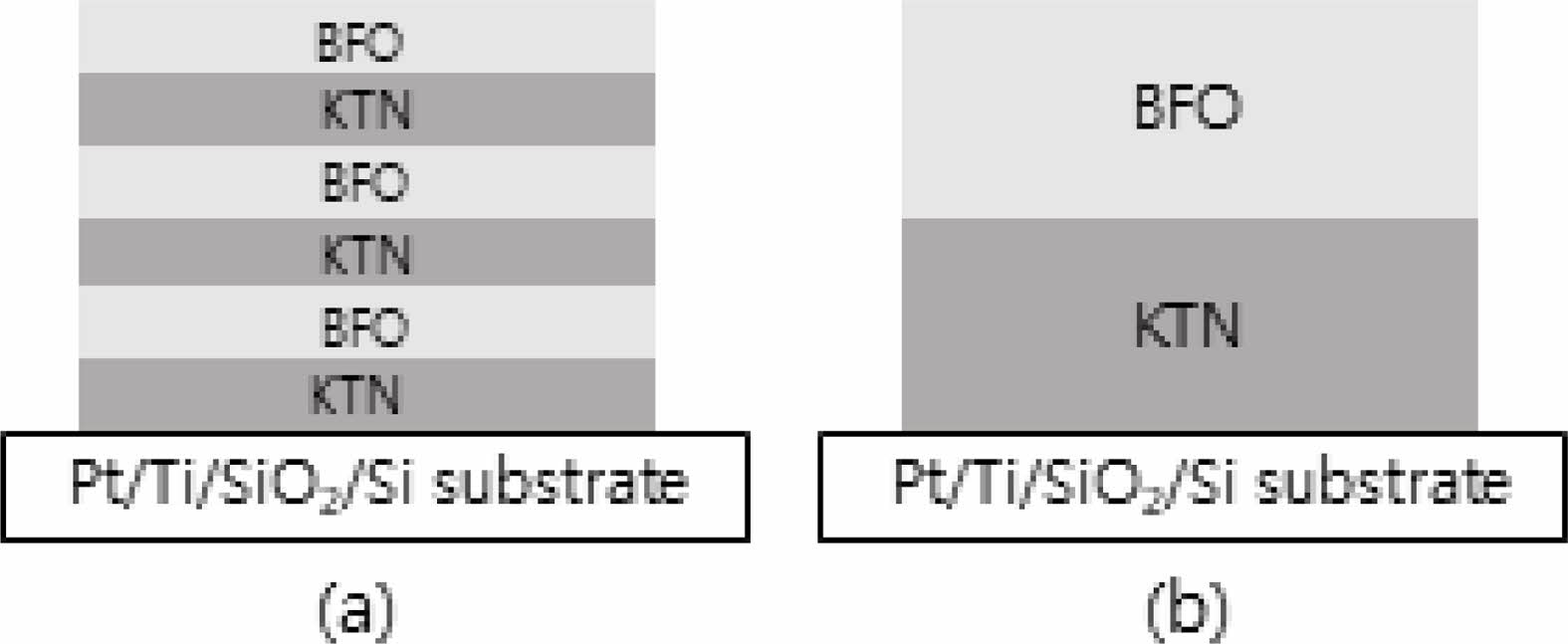
KTa0.62Nb0.38O3 precursor solutions were synthesized using the sol-gel method with Ta-ethoxide, Nb-ethoxide, and K-ethoxide in a dry nitrogen atmosphere. BiFeO3 precursor solutions were synthesized from Bi-nitrate pentahydrate and Fe-nitrate nonahydrate. The Sol-gel processes for preparing KTN and BFO precursor solutions were carried out similarly to a previous experiment [11]. KTN precursor solutions were coated on Pt/Ti/SiO2/Si substrate using spin-coating method, dried at 200 oC for 5 minutes, and thermally decomposed at 400 oC for 10 minutes. After spin-coating the BFO precursor solution on the KTN layer, drying and heat treatment were performed under the same conditions. This process was repeated 6 times to produce 6-layers KTN/BFO multilayer thin films (Fig. 1(a)). Additionally, in order to examine the effect of the interface of the KTN/BFO multilayer films, 2-layer KTN/BFO thin films, coated with KTN and BFO precursor solutions three times each on substrates, were fabricated (Fig. 1(b)). The sintering temperature of the KTN/BFO multilayer films was 590-650 oC. Fig. 1 shows a schematic cross-sectional diagram of the KTN/BFO multilayer thin films. X-ray diffraction analysis, AES depth profile and microstructures were observed according to the sintering temperature and number of coatings of KTN/BFO multilayer thin films. P-E (polarization-electric field) hysteresis loops and EC properties were observed using a ferroelectric tester (RT-66B, Radiant Tech., Inc. USA).
|
Fig. 1 Schematic cross-sectional diagram of KTN/BFO multilayer thin films. |
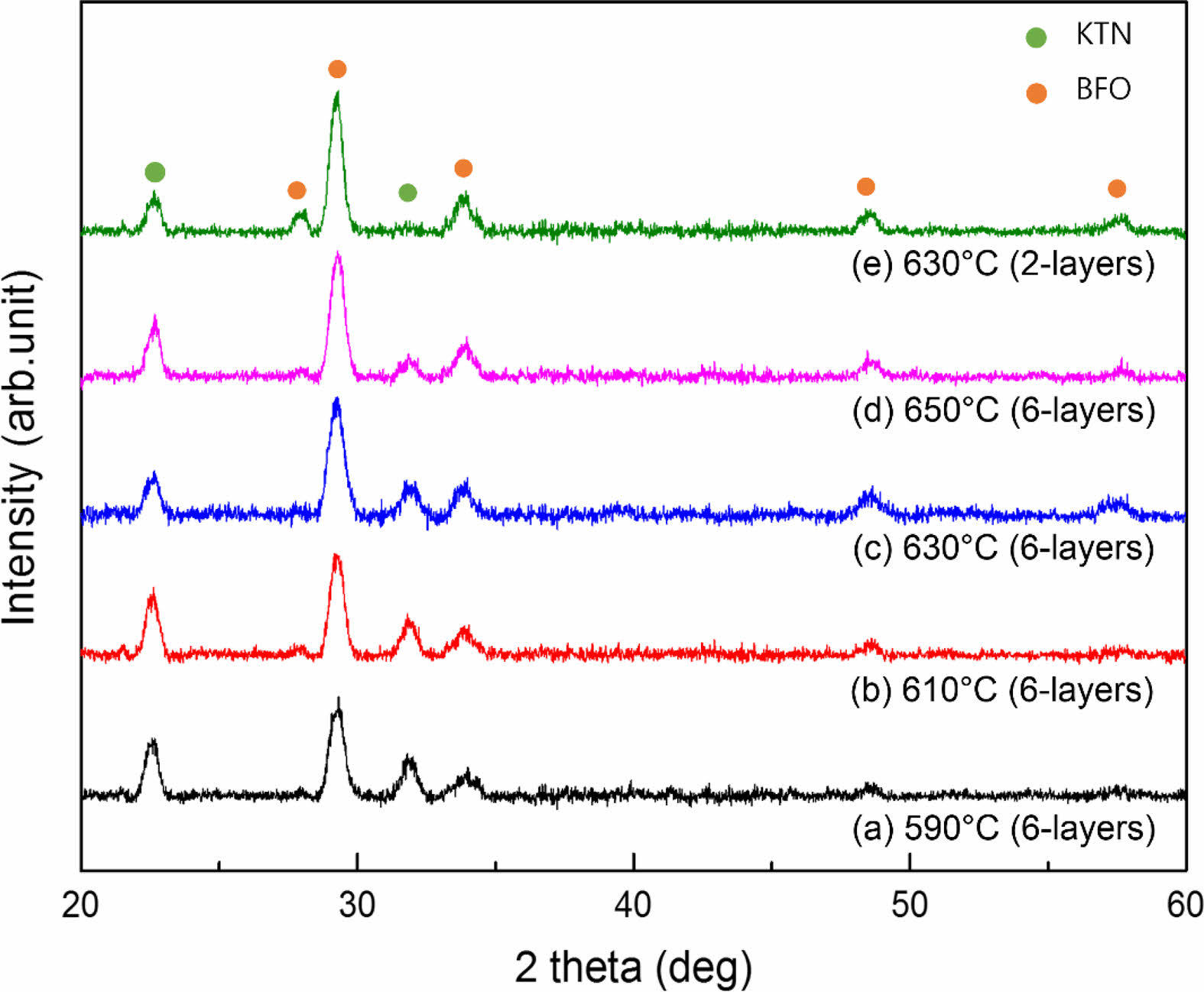
Fig. 2 shows the X-ray diffraction (XRD) patterns of the KTN/BFO multilayer films. All specimens showed typical polycrystalline XRD patterns, and secondary phases due to volatilization of K ions were not observed. As the sintering temperature increased from 590 oC to 650 oC, the intensity of the XRD peaks increased and the FWHM (full width at half maximum) decreased, so that the crystallinity of the specimen was improved [12]. All KTN/BFO multilayer thin films in which a cubic phase KTN(62/38) layer and a rhombohedral phase BFO layers were alternately stacked, both XRD peaks of KTN phase and BFO phase were observed with no preferential orientation. In the case of the 2-layer KTN/BFO multilayer film with a thick upper BFO thin film, BFO diffraction peaks were observed to be relatively higher than that of the 6-layer KTN/BFO multilayer films.
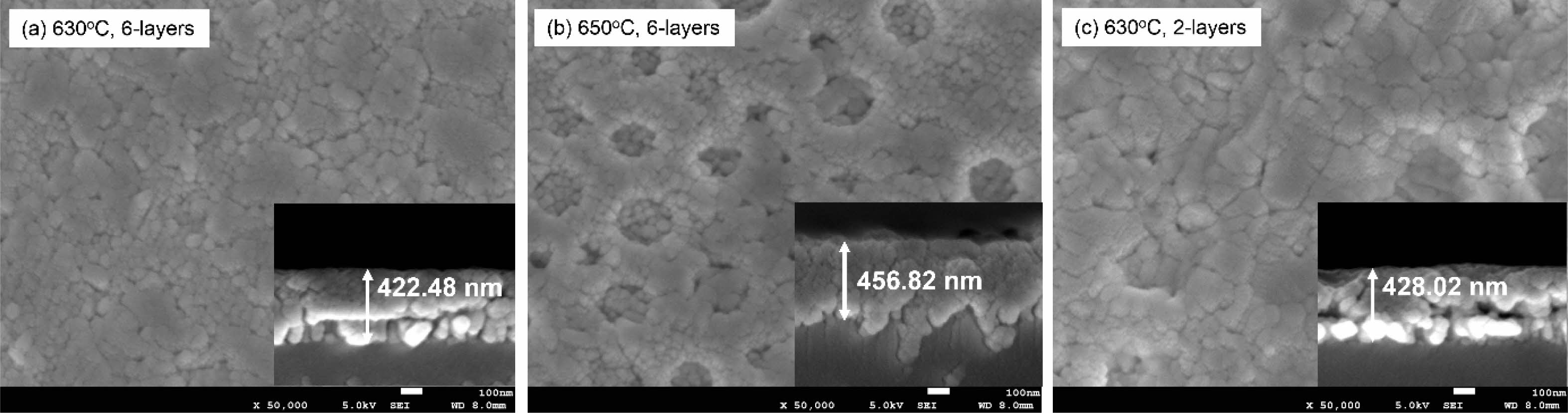
Fig. 3 shows the surface and cross-sectional micro- structure of the KTN/BFO multilayer films sintered at 630 oC and 650 oC. The 6-layer KTN/BFO films sintered at 630 oC (Fig. 3(a)) showed a dense micro- structure in which large and small grains were mixed. However, in the KTN/BFO multilayer films sintered at 650 oC (Fig. 3(b)), the interface between KTN/BFO film and substrate became rough, which is thought to be due to the diffusion of atoms by the high sintering temperature. The 2-layer KTN/BFO multilayer film sintered at 630 °C (Fig. 3(c)) showed a dense micro- structure with a relatively uniform grain size. Average thickness of the KTN/BFO multilayer films sintered at 630 °C was about 420 nm.
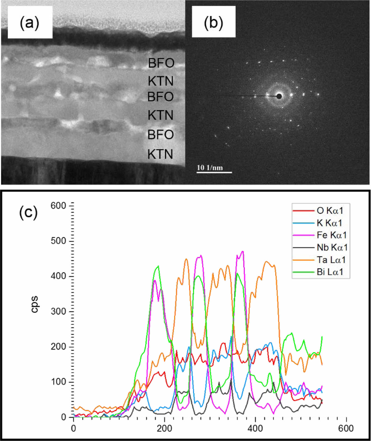
Fig. 4 shows the cross-sectional TEM microstructure (a), selected area electron diffraction (SAED) (b), and AES depth profiles (c) of the 6-layer KTN/BFO multilayer films sintered at 630 oC. The inside of the KTN/BFO multilayer thin film showed a dense microstructure without pores (Fig. 4(a)), and the KTN and BFO layers were clearly observed. The appearance of many spot-patterns in the SAED pattern is believed to be due to the distribution of KTN, BFO phases, and mixed phases distributed at the KTN/BFO interfaces (Fig. 4(b)). Non-uniform AES depth profiles for the elements of KTN/BFO multilayer film were shown due to differences in composition corresponding to KTN and BFO layers, and a diffusion of K, Ta, Nb, Fe, and Bi atoms was observed in adjacent layers (Fig. 4(c) [13].
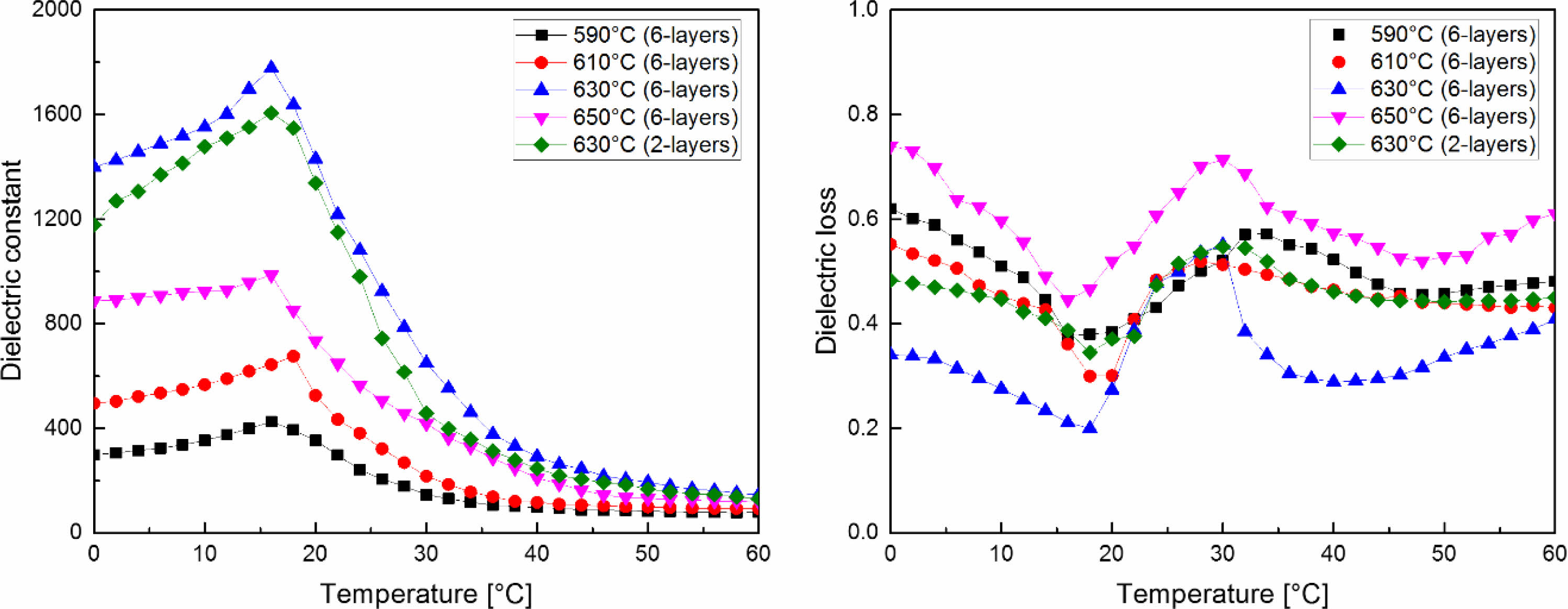
Fig. 5 shows dielectric constant and dielectric loss of the KTN/BFO multilayer films according to temperature variation. As the sintering temperature increased, the dielectric constant tended to increase, with the maximum value occurring in the film sintered at 630 oC. There was a slight decrease when the film was sintered at 650 oC. This is thought to be because the size of the ferroelectric grains, with a high dielectric constant, increased as the sintering temperature increased. However, in the case of sintering at 650 oC, it is believed that secondary phases with low dielectric constant were formed as the diffusion of atoms to the lower substrate increased, as shown in Fig. 3 [14]. Curie temperature was observed at about 16 oC in all KTN/BFO multilayer thin films. Dielectric constant and dielectric loss of the 6-layer KTN/BFO multilayer film sintered at 630 oC were 1380 and 0.384 at 20 oC, respectively.
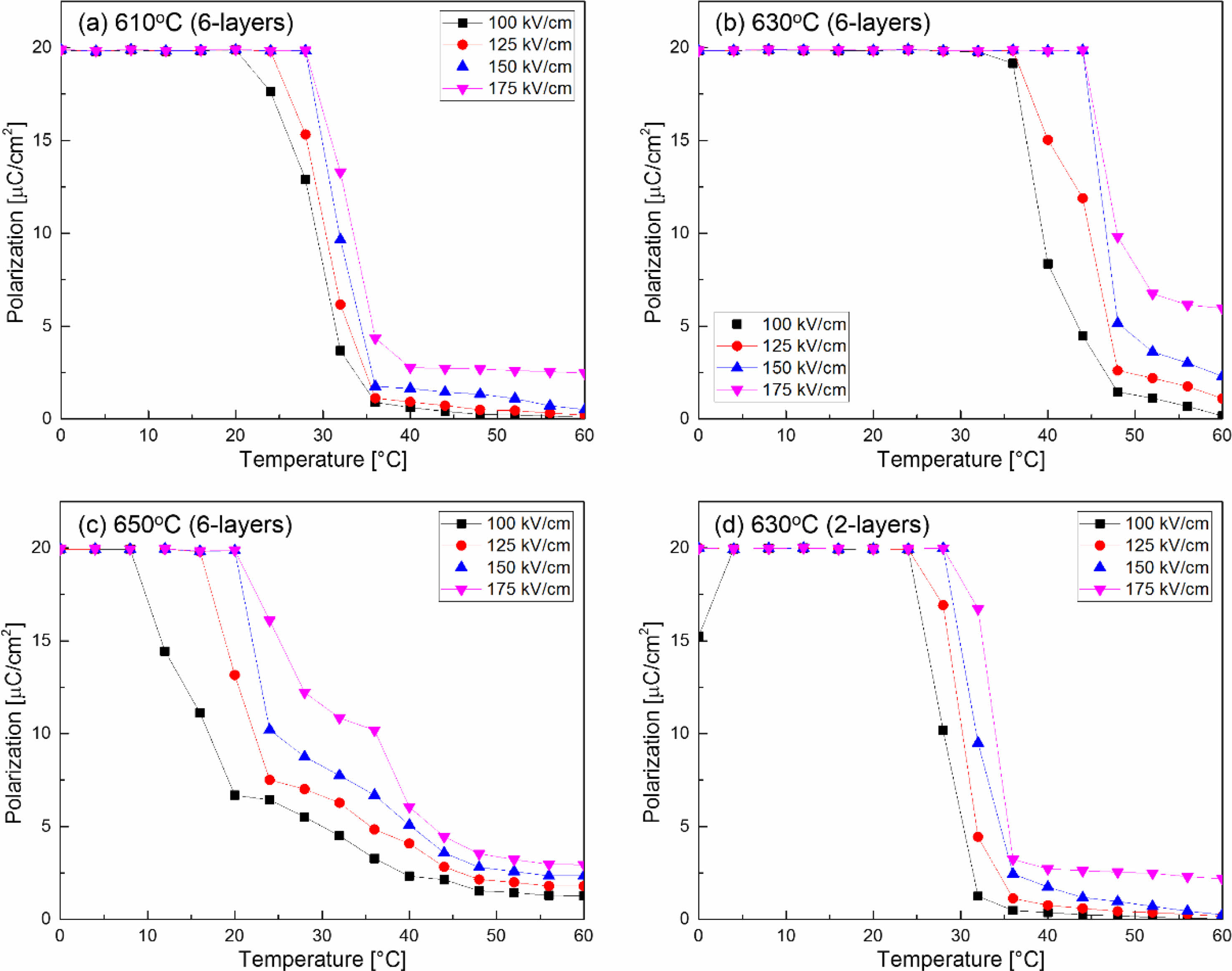
Fig. 6 shows the remanent polarization of the KTN/BFO multilayer films with variations of temperature and applied field. As the sintering temperature of the 6-layer KTN/BFO multilayer films increased, the temperature at which the remanent polarization decreased shifted higher, and diffusion phase transition was showed. These are believed to be due to an increase in ferro- electric grain size as sintering temperature increases, and the diffusion of atoms to adjacent KTN and BFO layers [15]. In the case of the 2-layer KTN/BFO thin film sintered at 630 oC, the phase transition were observed in a narrow temperature range, which is considered to be because the number of interfaces between KTN and BFO layer was smaller when compared to the 6-layer KTN/BFO multilayer films. As the applied DC electric field increased, the phase transition temperature tended to move higher, because the switching of the dipoles inside unit cell was suppressed [16].
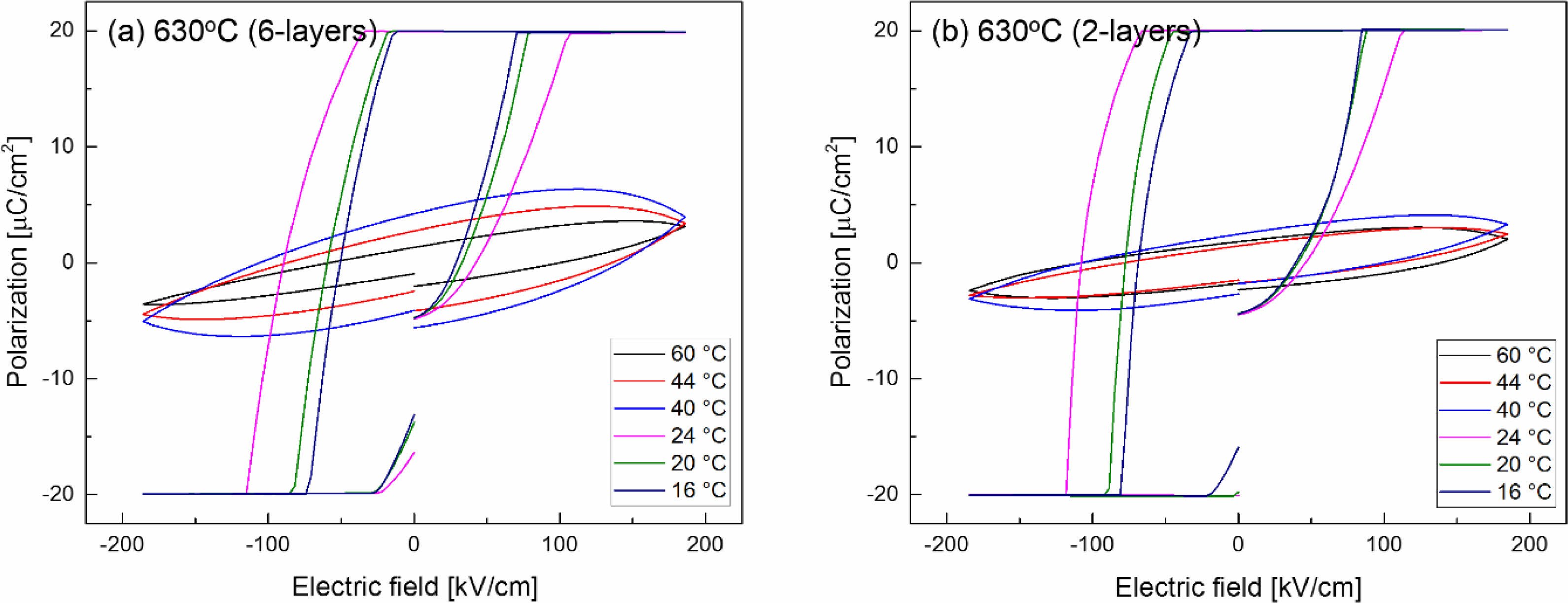
Fig. 7 shows the P-E hysteresis loops of the 2-layer and 6-layer KTN/BFO multilayer films sintered at 630 oC. The coercive fields of the 2-layer and 6-layer KTN/BFO multilayer films were 72.6 and 80.4 kV/cm at room temperature, respectively. The coercive fields decreased as the number of coatings increased. It is believed that this is due to interfacial layers that were formed at the interfaces of the KTN and BFO layers that acted as buffer layers to polarization switching [17].
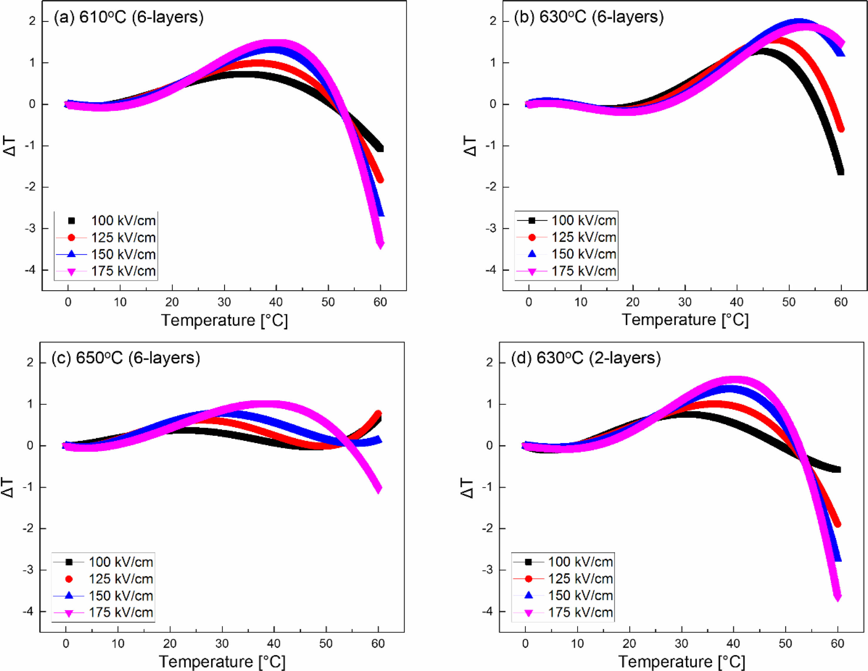
Fig. 8 shows the EC effect (ΔT) of KTN/BFO multilayer films. As the sintering temperature and the number of coatings increased, ΔT increased because of the increase in the ferroelectric grain size and remanent polarization due to interfacial polarization. ΔT was maximized at around 40-50 oC, which is slightly higher than Curie temperature. This is thought to be because ion displacements were easily changed by the applied electric field and temperature change as the ferro- electric and paraelectric phases attempt to coexist [18]. The ΔT and EC coefficients (∆T/∆E) of the 6-layer KTN/BFO multilayer film sintered at 630 oC were 1.96 oC and 0.13×10⁻⁶ oCmV-1, respectively. KTN/BFO multilayer films exhibited better ∆T than that of the lead-free (Ba,Sr)TiO3 film at an applied electric field of 158 kV/cm [19].
|
Fig. 2 X-ray diffraction (XRD) patterns of KTN/BFO multilayer thin films. |
|
Fig. 3 Surface and cross-sectional microstructures of the KTN/BFO multilayer films sintered at 630 oC and 650 oC. |
|
Fig. 4 (a) Cross-sectional TEM microstructure, (b) selected area electron diffraction (SAED), and (c) AES depth profile of the 6- layers KTN/BFO multilayer film sintered at 630 oC. |
|
Fig. 5 Dielectric constant and dielectric loss of KTN/BFO multilayer films with the variation of temperature. |
|
Fig. 6 Remanent polarization of KTN/BFO multilayer films with the variations of temperature and applied field. |
|
Fig. 7 P-E hysteresis loops of 2-layers and 6-layers KTN/BFO multilayer films sintered at 630 oC. |
|
Fig. 8 Electrocaloric effect (ΔT) of KTN/BFO multilayer films. |
KTN (62/38) and BFO precursor solutions were synthesized using the sol-gel method, and the KTN/BFO multilayer films were prepared using the spin-coating method. As a result of the AES depth profile, a non-uniform element profile was found due to the difference in composition of the KTN and BFO layers, and a diffusion of K, Ta, Nb, Fe, and Bi atoms into adjacent layers was observed. As the sintering temper- ature increased, the temperature at which the remanent polarization decreased moved higher, and showed diffuse phase transition characteristics. All specimens showed typical ferroelectric hysteresis loops. The ΔT increased with increasing the sintering temperature, and showed a maximum value around 40-50 oC, which is slightly higher than Curie temperature. KTN/BFO multilayer thin films fabricated through this study exhibits good electrocaloric properties of about 1.96 oC near room temperature, so it is expected that it can be applied as micro cooling devices. Using ferroelectrics with different crystal structures and electrical properties, it is thought that excellent electrocaloric properties can be realized through control of the crystallographic properties and the polarization mechanism at the interface of the multilayer thin films.
This research was supported by Basic Science Research Program through the National Research Foundation of Korea (NRF) funded by the Ministry of Education (2020R1A6A1A03038697) and This work was supported by the National Research Foundation of Korea (NRF) grant funded by the Korea government (MSIT) (2021R1I1A3052426).
- 1. A.S. Mischenko, Q. Zhang, J.F. Scott, R.W. Whatmore, and N. D. Mathur, Science 311 (2006) 1270-1271.
-

- 2. H. Maiwa, Jap. J. Appl. Phys. 56 (2017) 10PC05.
-
- 3. G. Catalan and J.F. Scott, Adv. Mater. 21 (2009) 2463-2485.
-
- 4. K. Yun, D. Ricinschi, T. Kanashima, and M. Okuyama, Appl. Phys. Lett. 89 (2006) 192902.
-
- 5. A. Moussavou, S. Deputier, V. Bouquet, M. Guilloux, A. Perrin, R. Sauleau, and K. Mahdjoubi, Ferroelectrics 362 (2008) 137-144.
-
- 6. M. Kwon, J. Kim, J. Park, and S. Lee, J. Ceram. Proc. Res. 21 (2020) 725-730.
-
- 7. O.M. Stafsudd and M.Y. Pines, J. Opt. Soc. Am. 62 (1972) 1153-1155.
-
- 8. H. Maiwa, Jap. J. Appl. Phys. 55 (2016) 10TB09.
-
- 9. Hang Ji and Ping Yu, Mater. Res. Express 8 (2021) 026303.
-
- 10. M. Kwon, S. Lee, K. Kim, and S. Choi, J. Ceram. Proc. Res. 20 (2019) 603-608.
-
- 11. B. Park, S. Lee, J. Kim, J. Park, and S. Lee, J. Ceram. Proc. Res. 22 (2021) 214-220.
-
- 12. A. Elghoul, A. Krichene, N. Boudjada, and W. Boujelben, Ceramics International 44 (2018) 12723-12730.
-
- 13. S. Jo, S. Lee, and Y. Lee, Nanoscale Research Lett. 7 (2012) 54.
-
- 14. S. Lee, K. Kim, and Y. Lee, Thin Solid Films 372 (2000) 45-49.
-
- 15. M. Shen, S. Ge, and W. Cao, J. Phys. D: Appl. Phys. 34 (2001) 2935-2938.
-
- 16. B.S. Semwal and P.K. Sharma, Canadian J. Phys. 51 (1973) 1874-1881.
-
- 17. S. Dutta, A. Pandey, I. Yadav, O.P. Thakur, R. Laishram, R. Pal, and R. Chatterjee, J. Appl. Phys. 112 (2012) 084101.
-
- 18. Y.P. Shi and A.K. Soh, Acta Materialia, 59 (2011) 5574-5583.
-
- 19. T. Ymamada, S. Matsuo, T. Kamo, H. Funakubo, M. Yoshino, and T. Nagasaki, J. Jap. Appl. Phys. 56 (2017) 10PF15.
-
 This Article
-
2022; 23(5): 583-588
Published on Oct 31, 2022
- 10.36410/jcpr.2022.23.5.583
- Received on Jan 11, 2022
- Revised on Apr 22, 2022
- Accepted on May 4, 2022
Services
- Abstract
introduction
experimental
results and discussion
conclusions
- Acknowledgements
- References
- Full Text PDF
Shared
Correspondence to
- Sung-Gap Lee
-
Dept. of Materials Engineering and Convergence Technology, RIGET, Gyeongsang National University, Jinju 52828, Korea
Tel : +82-10-2686-4427 Fax: +82-55-772-1689 - E-mail: lsgap@gnu.ac.kr
Clean-Energy Research Institute(CRI), Hanyang University, 222, Wangsimni-ro, Seongdong-gu, Seoul, 04763, Korea
E-mail: jcpr@hanyang.ac.kr