- Structural, physical and electrical properties of SiO2 thin films formed by atmospheric-pressure plasma technology
Kyoung-Bo Kima and Moojin Kimb,*
aDepartment of Materials Science & Engineering, Inha Technical College, Incheon 22212, Republic of Korea
bDepartment of Electronic Engineering, Kangnam University, Yongin 16979, Republic of KoreaThis article is an open access article distributed under the terms of the Creative Commons Attribution Non-Commercial License (http://creativecommons.org/licenses/by-nc/4.0) which permits unrestricted non-commercial use, distribution, and reproduction in any medium, provided the original work is properly cited.
Atmospheric pressure plasma (APP) systems operate at atmospheric pressure and low temperatures, eliminating the need for vacuum systems such as vacuum chambers and pumps. In this paper, we studied that silicon dioxide thin films were formed at room temperature (25 oC) and 400 oC by APP processes on silicon wafers. A mixture of hexamethyldisilazane, oxygen, helium, and argon was supplied to the plasma apparatus to form the SiO2 layer. It was observed that a heat insulating layer having a thickness of about 22 nm at 25 oC and about 75 nm at 400 oC was formed. Although the surface was clean in samples treated at 400 oC, small grains were observed in samples processed at room temperature. However, no void or defect in all samples is observed inside the thin film from the surface. The physical property of the SiO2 thin film carried out by measuring refractive index and density. The experimental refractive index of silicon dioxide grown by applying heat can be fitted to the Sellmeier equation. Also, the film density of the sample at 400 oC using a XRR was observed to be 2.25 g/cm3, similar to that of the glass, but that of the sample treated at room temp. was very low at 1.68 g/cm3. We also investigated the voltage-dependent current change in the oxide material. The SiO2 layer coated at room temperature showed a breakdown electrical field of 2.5 MV/cm, while oxides deposited at 400 oC showed a characteristic of 9.9 MV/cm
Keywords: Silicon oxide, Atmospheric pressure plasma, Hexamethylidisilazane, Room temperature, 400 oC
Micro- or nano-scale materials such as metals, semi- conductors, dielectrics or metal-dielectric film composites have been applied to electronic device technology due to their superior properties [1-6]. A dielectric thin film, like silicon nitride, aluminum oxide, and silicon dioxide (SiO2), have been applied to mass production during the past few decades in electronic devices [7-10]. In particular, SiO2 insulating layer is widely used interlayer and intermetal dielectrics, because of its high resistivity and its good adhesion to Si. The electrical resistivity of this film is close to ideal bulk values [11, 12], and same time it is stable and cost-effective.
Chemical vapor deposition (CVD) method is suitable for depositing of an insulating layer on the conductive and rough surface of steel, glass, and wafer due to its satisfactorily uniform coverage and relatively low process temperature [13-15]. Therefore, the CVD is one of the most developed methods for depositing of SiO2 thin film. In particular, the CVD technology affects the properties of amorphous thin films such as band gap, breakdown voltage, and surface morphology. Because of these physical properties, it can be widely used as an anti- reflection coating or passivation layer in the microelec- tronics industry.
Atmospheric pressure plasma (APP), a gas ionized in an atmospheric pressure atmosphere, is a technology that can efficiently treat silicon wafer, metal, and glass surfaces. Atmospheric plasma systems operate at atmospheric pressure and low temperatures, eliminating the need for vacuum systems such as vacuum chambers and pumps [16, 17].
It is usually obtained when a gas is excited to a state of energy through electrons in high frequency (rf), microwave or hot filament discharge. In particular, APP treatment process can generate a uniform high density plasma by utilizing a wide range of inert and reactive gases [18, 19]. Also, this technique is a very fast processing method compared to the technique performed in a vacuum chamber.
A similar experiment was performed before, but only the chemical properties of the thin film were observed, and no electrical analysis was performed [20, 21]. In order to apply the coated thin film to the field of electronic devices, characteristics according to voltage and current must be investigated. Therefore, this paper is intended to study the physical, electrical and morphological properties of SiO2 thin films formed on silicon wafers using APP technology for roll-to-roll manufacturing.
In order to form the SiO2 films, silicon wafer with a size of 27 × 27 mm2 was used. The film coating process is as follows. First, to remove dust and organic material on the wafer surface, oxygen plasma was generated by APP, which disappears through a physical and chemical reaction with plasma. The process was performed for 60 s with a power of 150 W. We observed that the surface changed from hydrophobic to hydrophilic by measuring the contact angle before and after oxygen plasma treatment. Next, the SiO2 thin layer was formed by repeatedly moving back and forth a total of 40 times at a speed of 10 mm per second while maintaining the temperature of the sample stage at room temperature (25 ℃) and 400 oC, respectively. To generate the plasma, a capacitively coupled APP is formed by a 13.56 × 10⁶ Hz radio frequency. The gas was supplied to the equipment through a small space between the power electrode and ground. HMDS (Hexamethylidisilazane, Merck Co., purity 99%, ((CH3)3SiNHSi(CH3)3) as the silicon precursor was fed to the plasma head by injecting Ar into the form of bubbles through a HMDS liquid tank stored at 60 oC. A mixture of HMDS/O2 (10 sccm)/He (10 lpm)/Ar (0.2 lpm) was composed to form the SiO2 layer. He/Ar is a plasma source and O2 is supplied for an oxidation of Si.
To evaluate the electrical properties of the SiO2 layer, the Ag metal film was formed using electron beam (E-beam) equipment and metal masks, with a thickness of 1000 Å and a diameter of 1 mm. E-beam evaporation is processed in a vacuum chamber capable of depositing conductors such as silver and aluminum, and AZO (Aluminum Zinc Oxide) semiconductors. The equipment used in this work was composed of an evaporator and a 150 keV ion accelerator in the same chamber; so that the coating and ion beam processes could be conducted in situ without breaking the vacuum. The base pressure before processing and the operating pressure during processing are ~10-6 Torr and ~10-3 Torr, respectively. The process temperature was at 25 oC. Also, the substrate was rotated at 5 rpm to form a uniform film. The E-beam current value was adjusted to maintain the deposition rate of Ag at 1 Å/s. In this process, Ag films was deposited on the surface of the silicon wafer in contact with the 1mm hole of the metal mask.
Surface morphology was performed using scanning electron micoscopy (SEM, JEOL-JSM7000F) equipment. The thickness and composition of thin films were investigated by transmission electron microscope (TEM, JEOL-2200FS,) and energy-dispersive X-ray spectroscopy (EDS, JEOL-JSM7000F), and density was analyzed using X-ray reflectivity (XRR, Rigaku-MFM310). The refractive index of the thin films was measured using an ellipsometer (Wizoptics-alphaSE). In addition, the voltage and current characteristics were measured by probe station (Mstech-M5VC).
In this paper, we investigate the experiment and the results of the APP process at 25 oC and 400 oC. The reason for analyzing the results at 25 oC is that, if oxides can be deposited at room temperature, the insulating layer deposition process is possible on all flexible or rollable materials that have recently become an issue in the field of electronic devices. Also, the reason for the additional comparative analysis of the 400 oC process is that the CVD process temperature condition used to deposit SiO2 currently used for mass production is about 400 degrees.
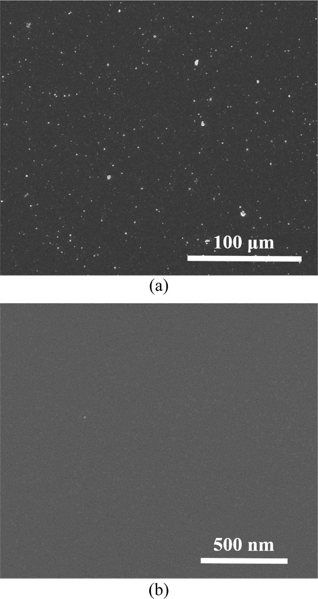
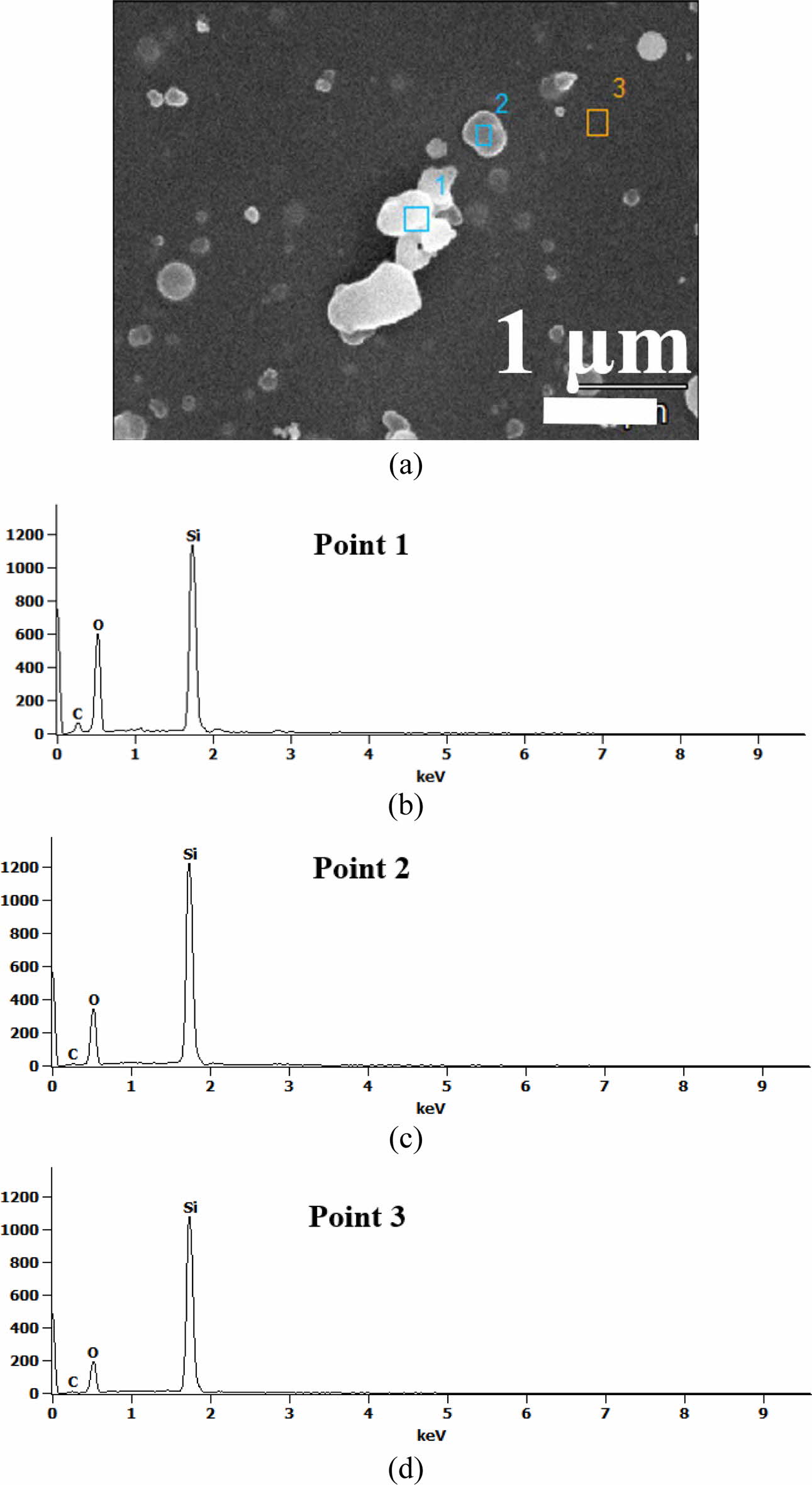
Fig. 1 shows SEM images of silicon dioxide deposited on silicon wafers by supplying HMDS to APP systems. Although the surface was clean in samples treated at 400 oC, small grains were observed in samples processed at room temperature. These increase the roughness of the film and weaken the adhesion with the film to be formed later. In Fig. 2, EDS analysis to investigate the compositional components of the film revealed that they were composed of silicon and oxygen. However, in the sample treated at room temperature, this pheno- menon affects the generation of particles and electrical characteristics in manufacturing electronic devices. In conclusion, it will have a direct impact on mass production yield. In previous studies, SiO2-like thin films were deposited at low temperature (< 50 oC) using APP technology. In detail, the film characteristics were investigated according to the HMDS and O2 flow rates. Compared to our chemical analysis, silicon, oxygen and carbon were detected except for hydrogen. The reason that no hydrogen was detected in our EDS data is due to the resolution limitations of the analytical equipment. To reduce carbon, which is an impurity in the thin film, a study was performed on the surface morphology and chemical bonding. However, the physical and electrical properties of the thin film were not analyzed.
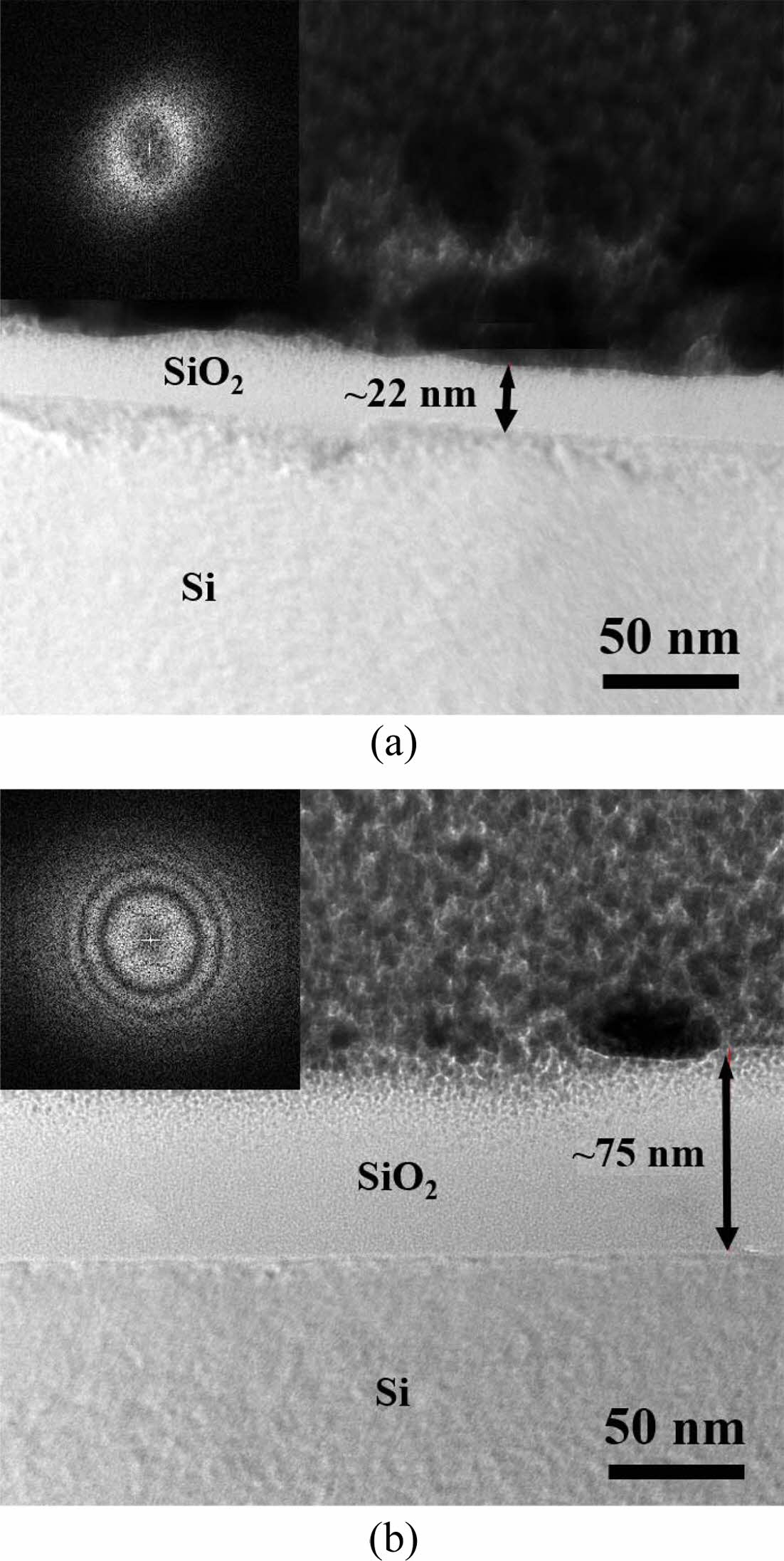
Next, we study the deposition rate according to the temperature and the shape of the inside of the thin film. Figs. 3(a) and 3(b) show the cross-sectional high resolution TEM results of silicon dioxide formed at 25 oC and 400 oC. It can be observed that an insulating layer having a thickness of ~22 nm at room temperature and ~75 nm at 400 oC was formed. The temperature difference of more than 350 oC resulted in a thickness difference of more than 3 times. In the APP equipment, if the sample stage is repeated once and again at 400 oC, a 1.9 nm SiO2 film is formed, whereas at room temp. 0.55 nm is deposited. No void or defect is observed inside the thin film from the surface of Fig. 1(b) and the TEM photograph, and these results indicate that dense SiO2 material was formed. The amorphous inorganic layer, devoid of micro-crystallites, was identified by weak and wide rings in the diffraction pattern by transmission electrons [See insets in Fig. 3]. The boundaries between the oxide material and the Si wafer were clear and a finite thickness interface was identified regardless of the temperature. Silicon and oxide are well bonded to each other, so it can be seen that oxide is an optimal insulating material for silicon semiconductors.
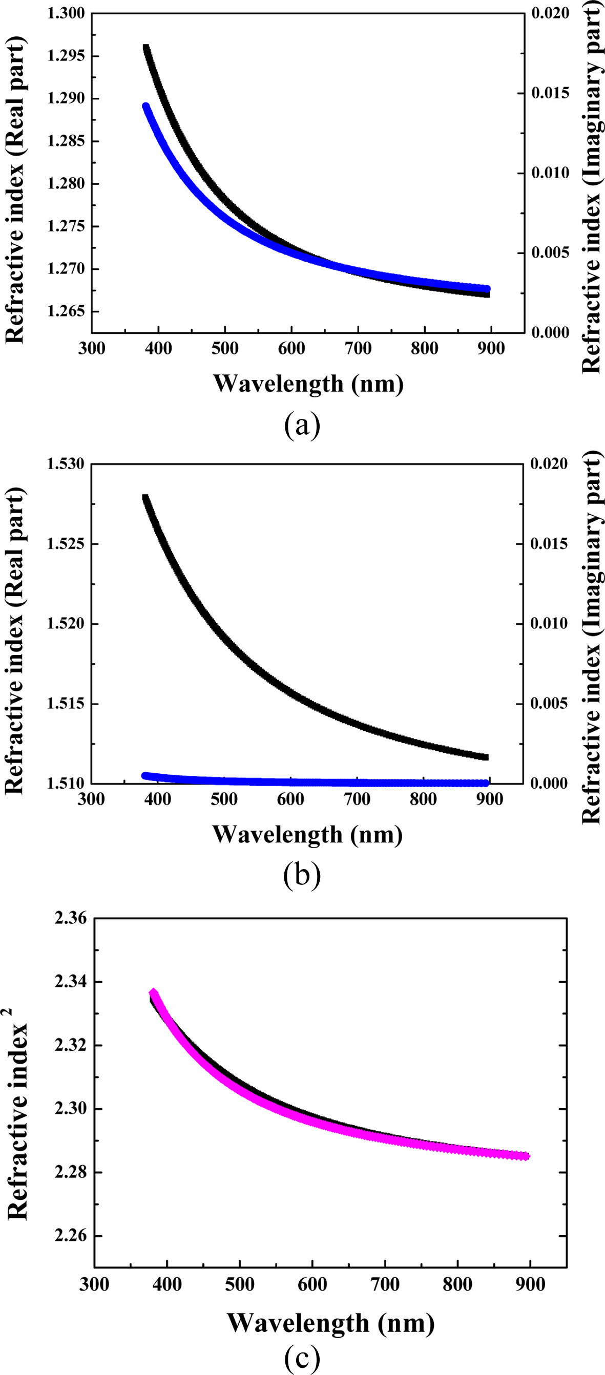
The physical properties of materials deposited at different temperatures were measured using ellipsometer (alpha-SE) and XRR (Rigaku, MFM310) as shown in Figs. 4 and 5. The refractive indices (n) of the insulating layer were determined for the light over the wavelength range from 400 nm to 900 nm by using an ellipso-meter. Figs. 4(a) and 4(b) indicate the real and imaginary parts of the refractive index over the measured wavelength range. The material coated at room temperature showed a small refractive index and an imaginary value related to the absorption rate was observed. This phenomenon is caused by the presence of defect due to incompletely coupled silicones or oxygen, resulting in the presence of energy bands in the bandgap [22]. When this charac- teristic is applied as an insulating layer to an opto- electronic device, the efficiency decreases due to light absorption, so the smaller this value is, the better. Samples fabricated by applying heat have very small imaginary part values, which means that they exhibit low light absorption due to low defect concentration. For application to an electronic device, it is necessary to implement process conditions in which the real part of the refractive index can be increased and the imaginary part can be decreased.
In particular, the silicon oxide film grown by applying heat was investigated in more detail, as below. The experimental refractive index of silicon dioxide can be fitted to the Sellmeier equation [5, 23].

The fitted curve is also shown graphically in Fig. 4(c), indicating that it matches the measurement value well. The fitted parameters are α = 2.277, β = 0.0014, γ = 0.084, δ = 0.0048, and ε = 0.015. The sum of the squared residuals for the fitted curve is very small. This means that the expression of Sellmeier's formulation is reasonable in the range of visible spectra.
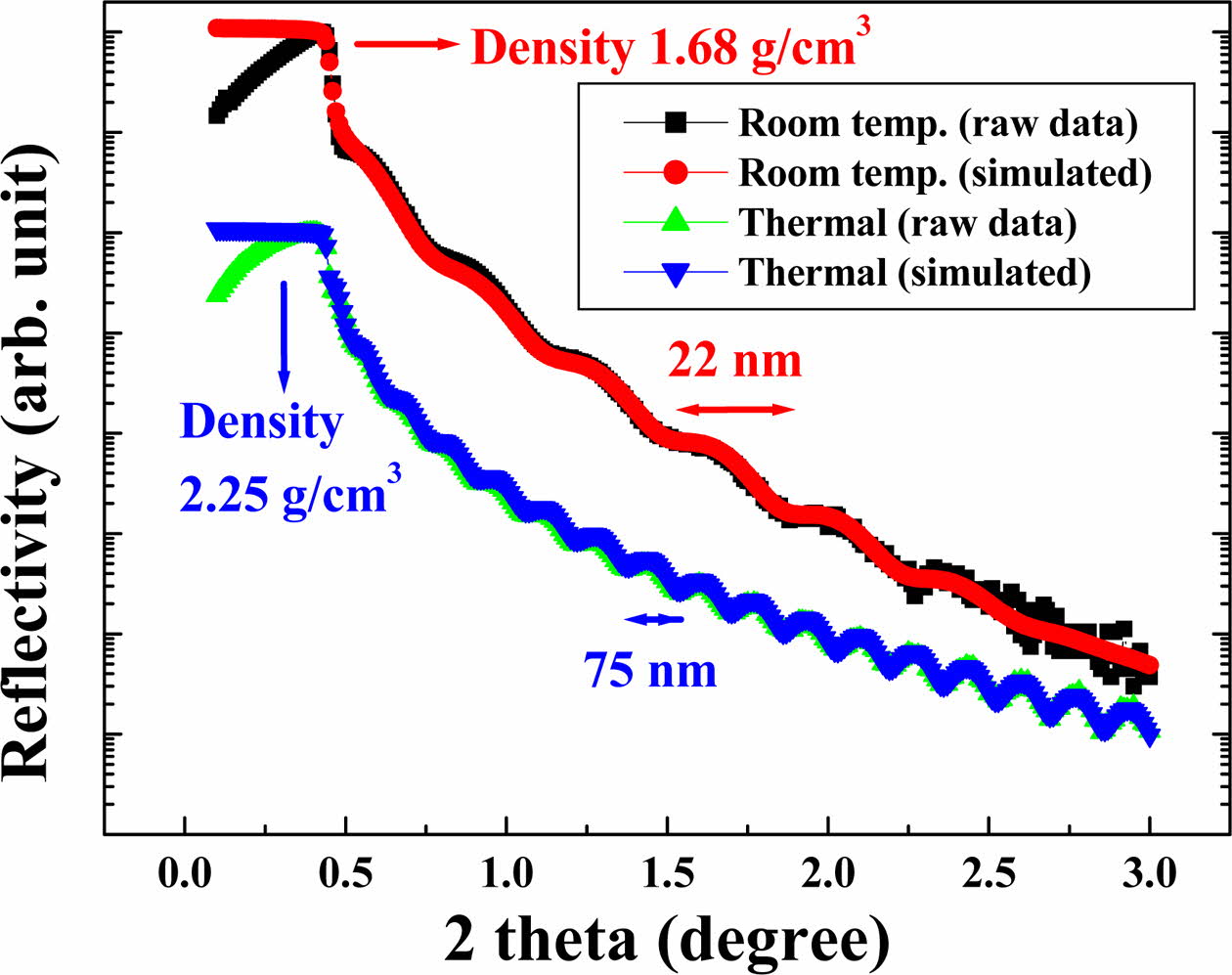
Also, the film density of the sample at 400 oC in Fig. 5 using a XRR was observed to be 2.25 g/cm3, similar to that of the glass, but that of the sample treated at room temp. was very low at 1.68 g/cm3. This means that the SiO2 thin film deposited by thermal conditions is denser than that deposited at low temperatures. The influence of the thickness should be considered, but it can be seen that about 0.6 g/cm3 is a very large difference. Through this analysis, the thickness of the oxide film was additionally measured, and the thickness of the heat treatment sample was 75 nm and the room temperature sample was 22 nm, which was almost identical to that of TEM in Fig. 3. Through the refractive index and XRR analysis results of the SiO2 film deposited at 400 oC, it can be expected that the physical properties of the thin film can be applied to optoelec- tronic devices.
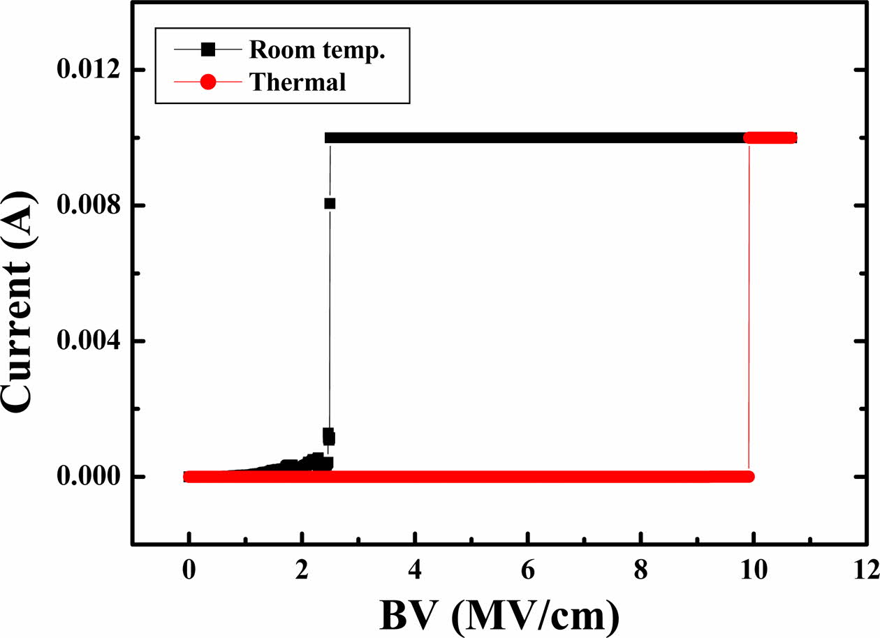
In order to evaluate the possibility of using the manufactured oxide film as a gate insulating layer of a thin film transistor or an insulating film for other uses in the semiconductor or display industry, voltage and current characteristics analysis is required. Current characteristics according to voltage were measured to verify the possibility of using the insulating layer of the electronic device, as shown in Fig. 6. The electrical breakdown of the SiO2 formed on the Si wafer can cause irreversible damage in the layer and seriously degrade the device performance [24, 25]. The breakdown field BV is expressed by the BV = Vbd/t where Vbd is the value of the breakdown voltage and t is the thickness of the SiO2, while the sharp increase in current indicates the electrical failure of the layer. As shown in the figure, SiO2 coated at room temperature showed a breakdown electrical field of 2.5 MV/cm, while oxides deposited at 400 oC showed a characteristic of 9.9 MV/cm. The thin film produced by applying heat is similar to the BV characteristics of the oxide film deposited in mass production using the thermal oxidation method or CVD method [24]. However, the low BV value at room temp. is associated with low density and refractive index values, and is also affected by the small grains formed on the surface in the SEM image. This is because the electric field is concentrated on the sharp or protruding part.
|
Fig. 1 Plane-view SEM images of silicon dioxide processed at (a) room temperature and (b) 400 oC, respectively. |
|
Fig. 2 (a) Image of EDS analysis of samples formed at room temperature: The spectrum of (b) point 1, (c) point 2, and (d) point 3. |
|
Fig. 3 Cross sectional TEM images of silicon dioxide processed at (a) room temperature and (b) 400 oC, respectively. Insets indicates the diffraction pattern images by transmission electrons. |
|
Fig. 4 Real (black) and imaginary (blue) parts of the refractive index over the measured wavelength range of silicon dioxide processed at (a) room temperature and (b) 400 oC, respectively. (c) Measured refractive index versus wavelength (black) and fitted curves (pink) to the Sellmeier's formula. |
|
Fig. 5 Thickness and density of SiO2 thin films analyzed by simulating data (red and blue) measured (black) with XRR. |
|
Fig. 6 Current change according to function of electric field (E) of silicon dioxide processed at room temperature (black) and 400 oC (red), respectively |
Using APP technology and HMDS, a silicon oxide film was formed at room temperature and 400 oC, and the physical and electrical properties of the film were examined. The temperature difference of 375 oC resulted in a thickness difference of more than 3 times. In the APP equipment, if the sample stage is repeated once and again at 400 oC, a 1.9 nm SiO2 film is formed, whereas at room temp. 0.55 nm is deposited. No void or defect is observed inside the thin film from the surface.
The optical characterization of the SiO2 material was performed by measuring the refractive index. The ex- perimentally measured refractive index of this material deposited at 400 oC is well matched with the form of the Sellmeier's formula. In addition, SiO2 thin films deposited by thermal conditions are denser than thin films deposited at low temperatures.
The steady-state I-V characteristics have been studied for a wide range of applied electric fields. The SiO2 layer coated at room temperature showed a breakdown electrical field of 2.5 MV/cm, while oxides deposited at 400 oC showed a characteristic of 9.9 MV/cm. The low breakdown field at room temp. is associated with a low density value by the presence of defect due to incompletely coupled silicones or oxygen, resulting in the presence of energy bands in the bandgap.
In particular, the evaluation of the electrical pro- perties of the SiO2 thin film formed using atmospheric pressure plasma at room temperature was presented for the first time in this paper. The oxide film deposited at room temperature has no small grains on the surface and will establish process conditions for forming a film having excellent electrical and physical properties. In addition, the thin film formed at 400 oC showed a high breakdown electric field value of 9 MV/cm or more. These analysis results indicate that the SiO2 film, which is used as an important film for electronic devices such as displays and semiconductors, can be formed by atmospheric pressure plasma technology. In the future, we will apply the results of these techniques to insulating and oxide films for flexible electronic devices.
This work was supported by the National Research Foundation of Korea (NRF) grant funded by the Korea government (MSIT) (No. 2021R1F1A1046135).
Kyoung-Bo Kim and Moojin Kim contributed equally to this work.
- 1. H. Khachatryan, S.-N. Lee, K.-B. Kim, H.-K. Kim, and M.J. Kim, J. Phys. Chem. Solids 122 (2018) 109-117.
-

- 2. H. Khachatryan, S.-N. Lee, K.-B. Kim, and M.J. Kim, Metals 9 (2019) 12.
-

- 3. W.J. Dong, C.J. Yoo, H.W. Cho, K.-B. Kim, M.J. Kim, and J.-L. Lee, small 11 (2014) 1947-1953.
-

- 4. K.-B. Kim, M.J. Kim, H.-C. Lee, S.-W. Park, and C.-W. Jeon, Mater. Res. Bull. 85 (2017) 168-175.
-

- 5. M.J. Kim, J.H. Min, Y.S. Kwak, D.R. Kim, K.-B. Kim, and J.H. Song, Solid-State Electron. 129 (2017) 16-21.
-

- 6. K.-H. Kim and M.-H. Ri, J. Phys. Chem. C 122 (2018) 16281-16288.
-

- 7. Z. Krstic and V.D. Krstic, J. Mater. Sci. 47 (2012) 535-552.
-

- 8. M.D. Groner, F.H. Fabreguette, J.W. Elam, and S.M. George, Chem. Mater. 16 (2004) 639-645.
-

- 9. O.A. Dicks, J. Cottom, A.L. Shluger, and V.V. Afanas'ev, Nanotechnology 30 (2019) 205201.
-

- 10. D. Arl, V. Rogé, N. Adjeroud, B.R. Pistillo, M. Sarr, N. Bahlawane, and D. Lenoble, RSC Adv. 10 (2020) 18073-18081.
-

- 11. W. Zhu, G. Zheng, S. Cao, and H. He, Sci. Rep. 8 (2018) 10537.
-

- 12. A.-ur-Rehman, J.B. Lee, A. Qudoos, S.H. Jakhrani, H.G. Kim, and J.-S. Ryou, J. Ceram. Process. Res. 20 (2019) 270-275.
-

- 13. C.H. Jeong, J.H. Lee, J.T. Lim, N.G. Cho, C.H. Moon, and G.Y. Yeom, Jpn. J. Appl. Phys. 44 (2005) 1022.
-

- 14. Y.T. Kim, S.G. Yoon, H. Kim, S.J. Suh, G.E. Janga, and D.H. Yoon, J. Ceram. Process. Res. 6 (2005) 294-297.
- 15. S.H. Cho, Y.Y. Choi, Y.H. Kim, and D. J. Choi, J. Ceram. Process. Res. 11 (2010) 581-585.
- 16. J.A. Bittencourt, Fundamentals of plasma physics, 3rd ed. (Springer, 2004).
-

- 17. A. Schütze, J.Y. Jeong, S.E. Babayan, J.Y. Park, G.S. Selwyn, and R.F. Hicks, IEEE Trans. Plasma Sci. 26 (1998) 1685-1694.
-

- 18. H.-P. Kim, M.J. Kim, K.-B. Kim, H. Khachatryan, and J. Jang, Surf. Coat. Technol. 330 (2017) 228-233.
-

- 19. H. Khachatryan, H.-P. Kim, S.-N. Lee, H.-K. Kim, M.J. Kim, K.-B. Kim, and J. Jang, Mat. Sci. Semicon. Proc. 75 (2018) 1-9.
-

- 20. Y.S. Kim, J.H. Lee, J.T. Lim, J.B. Park, and G.Y. Yeom, Thin Solid Films 517 (2009) 4065-4069.
-

- 21. Y.S. Kim, J.H. Lee, Thuy.T.T. Pham, J.T. Lim, and G.Y. Yeom, J. Korean Phy. Soc. 53 (2008) 892-896.
-

- 22. R.E. Willoughby, M.I. Cotterell, H. Lin, A.J. Orr-Ewing, and J.P. Reid, J. Phys. Chem. A 121 (2017) 5700-5710.
-

- 23. A.A. Voronin and A.M. Zheltikov, Sci. Rep. 7 (2017) 46111.
-

- 24. M.J. Kim and G.H. Jin, J. Appl. Phys. 105 (2009) 074507.
-

- 25. M.J. Romero, K. Alberi, I.T. Martin, K.M. Jones, D.L. Young, Y. Yan, C. Teplin, M.M. Al-Jassim, P. Stradins, and H.M. Branz, Appl. Phys. Lett. 97 (2010) 092107.
-

 This Article
-
2022; 23(4): 535-540
Published on Aug 31, 2022
- 10.36410/jcpr.2022.23.4.535
- Received on Jul 15, 2021
- Revised on Mar 24, 2022
- Accepted on Apr 2, 2022
 Services
- Abstract
introduction
experimental and theoretical details
results and discussion
conclusion
- Acknowledgements
- Author Contributions
- References
- Full Text PDF
Shared
 Correspondence to
- Moojin Kim
-
Department of Electronic Engineering, Kangnam University, Yongin 16979, Republic of Korea
Tel : +82-31-280-3809 Fax: +82-31-281-3604 - E-mail: moojinkim7@kangnam.ac.kr


 Copyright 2019 International Orgranization for Ceramic Processing. All rights reserved.