


- Effect of different abrasive grain sizes of the diamond grinding wheel on the surface characteristics of GaN
Joo Hyung Leea, Seung Hoon Leeb, Hee Ae Leeb, Nuri Oha, Sung Chul Yib,c and Jae Hwa Parkd,*
aDivision of Materials Science and Engineering, Hanyang University, Seoul 04763, Korea
bCeramic research institute, Hanyang University, Seoul 04763, Korea
cDepartment of Chemical Engineering, Hanyang University, Seoul 04763, Korea
dAMES Micron Co. Ltd., Gimpo 10124, KoreaThis article is an open access article distributed under the terms of the Creative Commons Attribution Non-Commercial License (http://creativecommons.org/licenses/by-nc/4.0) which permits unrestricted non-commercial use, distribution, and reproduction in any medium, provided the original work is properly cited.
Gallium nitride (GaN) substrates were ground in two different grinding wheel abrasive sizes of 270 and 800-mesh, and the change in surface morphologies of the substrates and the depth of subsurface damage (SSD) were observed. With the 800-mesh grinding wheel, the surface roughness (SR) and the depth of SSD of the sample tended to decrease, which was not the case with the 270-mesh grinding wheel. In the X-ray rocking curve, the sample exhibited some compressive stress with the 270-mesh grinding wheel, but with the 800-mesh grinding wheel, it demonstrated the occurrence of tensile stresses in the sample and a decrease in full width at half maximum (FWHM), which confirms an improvement in the crystallinity. In the Raman spectra, the compressive stress of the 270-mesh grinding wheel and the tensile stress of the 800-mesh grinding wheel were confirmed through peak shifts. Photoluminescence (PL) spectra confirmed that the intensity ratio of the yellow luminescence increased at the 800-mesh grinding wheel, and a blue shift occurred further. These results indicate that the SR and the depth of SSD were proportional to the abrasive grain size of the grinding wheel. At the same time, the increase in PL intensity at specific peak positions indicates that the stress stemming from the grinding process was concentrated at the crystal surface. The above mechanism is illustrated in a schematic diagram, which confirms the possibility of improving the grinding efficiency and subsequent polishing processes in future applications
Keywords: Gallium nitride, Single crystal, Hydride vapor phase epitaxy, Grinding, Subsurface damage
Gallium nitride (GaN) has excellent properties such as a wide bandgap energy of 3.4 eV, high dielectric breakdown strength of 3.3 MV/cm, and high electron saturation velocity of 2.4 × 107 cm/s, and high temperature stability [1, 2]. It is, thus, a fascinating next-generation material that can be used in optical devices such as high-brightness light-emitting diodes (LEDs) and laser diodes (LDs), power devices, and radio-frequency (RF) devices [2, 3].
In the case of GaN single-crystal substrates, various defects occur during the growth or wafering processes. These defects cause electron and light scattering which causes quality degradation and hinders the application of these fields [4, 5]. Among the defects of GaN wafers, subsurface damage (SSD) layers are mainly produced by the wafering process and must be removed in the final wafering process [6, 7].
Grinding is a GaN wafering process that flattens the rough surface of an as-grown or as-sliced GaN single crystal by utilizing a grinding wheel rotating at high speed. This process makes the subsequent polishing process possible but produces a deep SSD [7]. In general, SSD resulting from the grinding process gradually undergoes a shortening of depth through subsequent polishing and is almost completely removed through chemical-mechanical polishing (CMP) or inductively coupled plasma-reactive ion etching (ICP-RIE) [7, 8]. However, deeper SSD depth implies that more wafering time is required for the polishing process, eventually resulting in additional process costs. This is one of the causes of the high cost of GaN wafers, making them difficult to commercialize [9]. There are previous studies to reduce SSD and stress originated from wafering pro- cesses by varying diamond abrasive size in mechanical polishing (MP) [10] or varying the conditions of CMP method [11], etching [12], or annealing process [13].
In this study, we attempted to compare the changes in the surface morphologies and SSD of GaN substrates based on differences in the grain sizes of the diamond abrasives constituting the grinding wheel. Based on the results of the analysis of the physical and optical pro- perties of the surface of the GaN single crystal that change owing to abrasive size, we attempted to deter- mine how SSDs are generated from the grinding process and how they affect the properties of the substrates. We applied these results to a grinding process to improve the efficiency of the GaN wafering process.
GaN single crystals (approximately 1.0 mm) were grown on a c-plane sapphire substrate under the same conditions using a homemade vertical hydride vapor-phase epitaxy (HVPE) reactor. A high-speed grinding machine (Engis, EHG-170AV, Korea) was used for the grinding process, and 270 and 800-mesh (abrasive grit) sizes were used. In this study, the average abrasive sizes of the 270 and 800-mesh diamond grinding wheels are approximately 53 µm and 18 µm, respectively. The grinding process was performed with a target depth of approximately 10 µm. The detailed grinding process conditions are listed in Table 1.
After grinding, surface morphologies of samples A and B were measured using a white-light interferometer (WLI; NanoSystem, NanoView E-Series, Korea) and scanning electron microscopy (SEM; Jeol, JSM-5900LV, Japan). The surface of the as-ground GaN single crystal was polished with a 3 µm diamond abrasive using a polishing machine (Engis, EK-380I, Korea) to observe surface changes according to the processing time. The polished specimens were observed using optical microscopy (OM; BiMeince, S39CM, Korea).
Samples A and B were sampled using focused ion beam field-emission SEM (FIB-FESEM; FEI, Scios, USA) to analyze the SSDs of the GaN single crystals; SSDs were observed using scanning transmission electron microscopy (STEM; Jeol, JEM 2100F, Japan). By measuring the X-ray rocking curve (XRC) of the high-resolution X-ray diffraction (HR-XRD; Rigaku, ATX-G, Japan), the peak shift and FWHM of the GaN single crystal were calculated after each grinding process and compared with the residual stress and crystallinity changes according to the SSD. The samples were measured using a micro-Raman spectrophotometer (JASCO, NRS-3100, England) at a laser wavelength of 534.0 nm and a power of 2.5 mW to analyze the residual stress and defects on the surface and subsurface. Photo- luminescence (PL; Dongwoo Optron, MonoRa750i, Korea) was used to evaluate the optical properties of the GaN samples. For PL, the laser power was 2.5 mW and a He-Cd laser with a wavelength of 325 nm was used at room temperature.
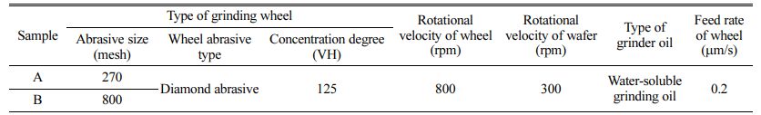
Fig. 1 shows a schematic diagram of the abrasives of the grinding wheel, along with WLI and SEM images of the surface and cross-section after the grinding process. Fig. 1(a) shows an image of the GaN substrates after grinding with the 270-mesh grinding wheel, and Fig. 1(b) shows an image of the substrates after grinding with the 800-mesh grinding wheel. Measuring the GaN surface with WLI, the maximum and minimum surface roughness (SR) values were found to be 8.5 mm (Fig. 1(a)) and 4.8 µm (Fig. 1(b)), respectively. When a grinding wheel with a larger mesh size was used, the SR value of the as-ground GaN decreased [14]. This can be observed in greater detail in the cross-sectional SEM images. From the SEM cross-sectional images, it can be seen that the smaller abrasive grit size of the grinding wheel results in lesser SR of the ground GaN. This is because the smaller abrasive grit size of the grinding wheel under the same conditions results in a smaller grinding depth into GaN.
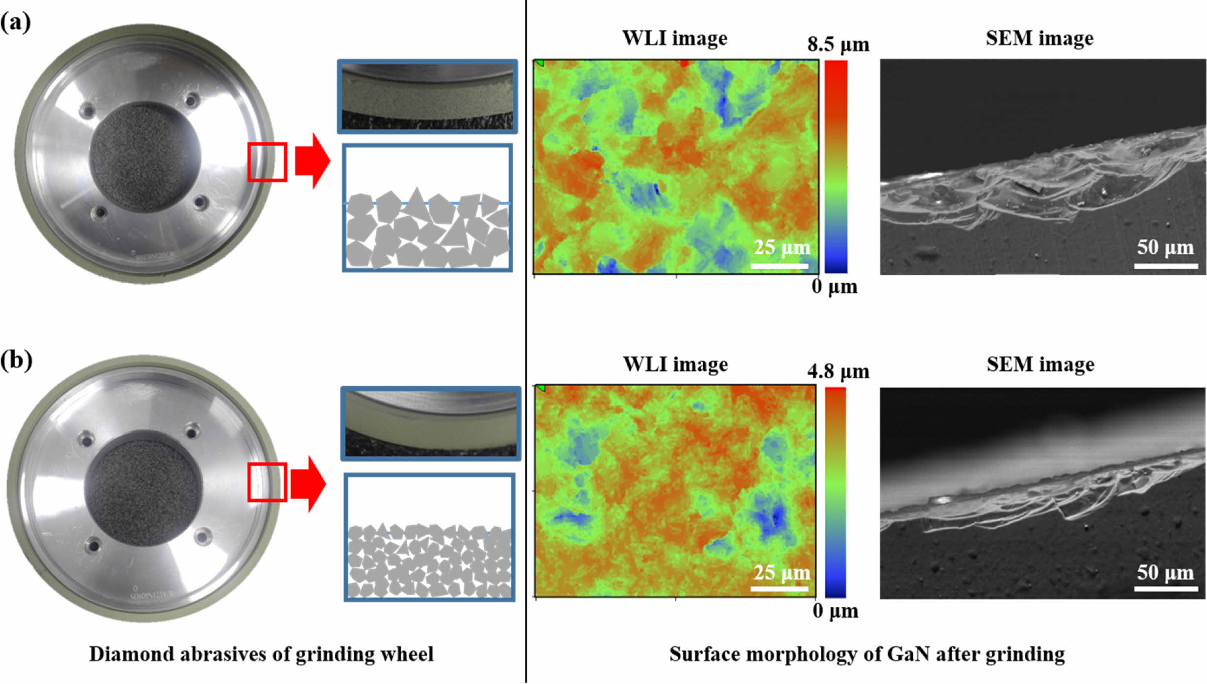
Fig. 2 shows an OM image of the polished GaN surface under the same conditions after grinding with wheels of different mesh sizes. Fig. 2(a) and (b) show OM images after grinding with the 270 and 800-mesh grinding wheels, respectively. In the polishing process, sample B took 120 min, which is shorter than the time required for sample A to remove ground surface defects such as scratches and micro-cracks. This indicates that the low SR value of sample B resulted in a shorter polishing time under the same conditions. These results confirm that the time required for the polishing process, which is the subsequent grinding process, was subject to the difference in the diamond abrasive size.
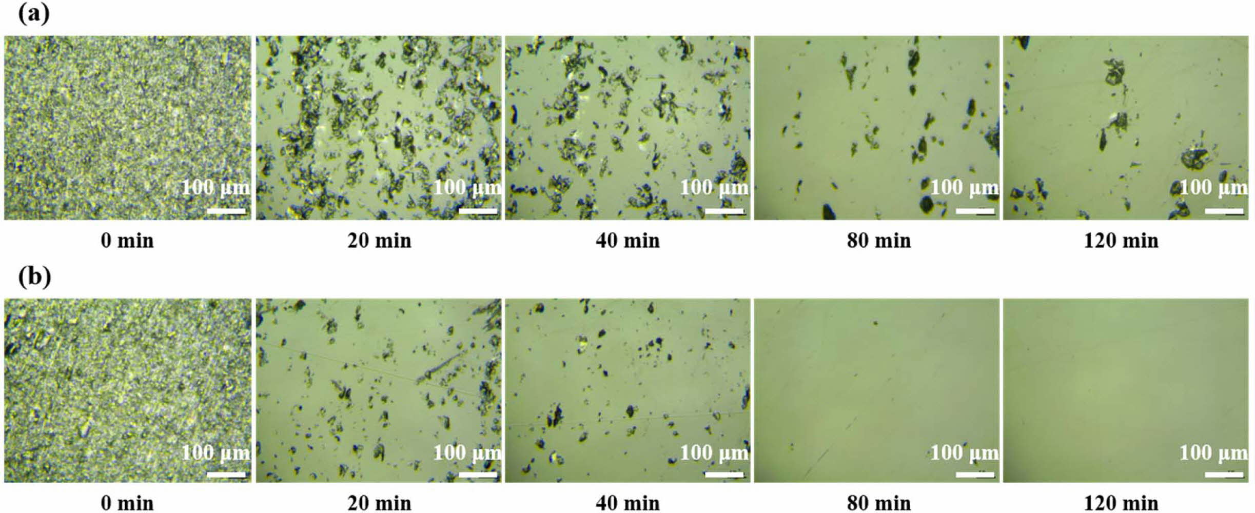
To analyze the internal defects caused by grinding, STEM was performed on the cross-sectional plane of the GaN substrates after each grinding process (Fig. 3). Fig. 3(a) and (b) show STEM images of the cross-sectional planes of GaN ground with the 270 and 800-mesh sizes, respectively. STEM measurements of the bright-field (BF) type were performed and based on the characteristics of the BF-STEM, the central electron beam and a small collection angle were measured. The measurement was done such that the area that was not scattered was measured brightly, and the area where phonon scattering occurred was measured darkly [15]. The damage layer produced during the grinding process acts as a defect and causes phonon scattering in the electron beam [15]. In the STEM image, a GaN single-crystal region in which only a few defects exist is relatively bright, and black regions unevenly distributed in the ground GaN surface region can also be seen. Fig. 3(a) and (b) show the damage layer from the surface to a certain depth. In the first figure, the damage layer was formed up to 1.050 μm thick in the grinding process using the 270-mesh grinding wheel, but the other using the 800-mesh grinding wheel had a 0.494 μm thick damage layer. Based on these results, it can be observed that the depth of the SSD decreases further when a finer grit size is used in the process, and the grain size of the grinding wheel affects not only the SR but also the depth of the SSD.
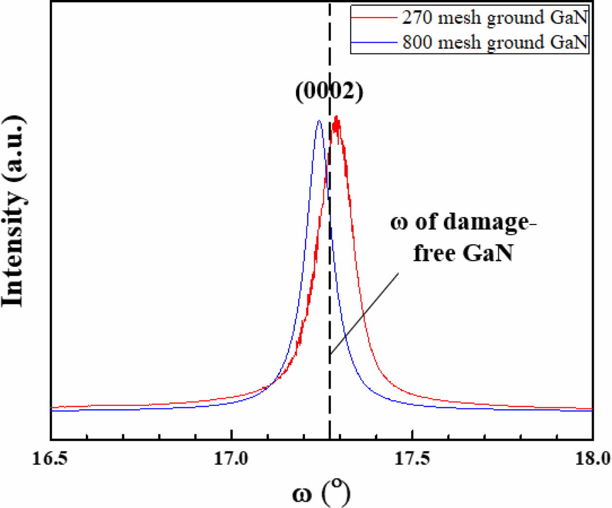
Fig. 4 shows the XRC measurements for the GaN substrates after the 270 and 800-mesh grinding processes with ω values of the (0002) peak angles appearing at 17.2911o and 17.2412o, respectively. Compared with the theoretical bulk GaN (0002) peak angle of 17.2833o, sample A of the 270-mesh grinding wheel shifted to the right, which means that the interplanar distance of the (0002) plane decreased according to Bragg's law, unlike the theoretical bulk GaN, and this can be interpreted as due to the presence of compressive stress within [16]. However, as the 800-mesh grinding shifts to the left based on the bulk GaN, it is judged that tensile stress exists inside. In theory, if the SSD generated by the grinding process is present within the material, compressive stress is induced owing to the strong lattice distortion [17]. Bulk GaN single crystals grown on sapphire are subjected to stress after cooling because of the difference between the lattice constant and thermal expansion coefficient with the heterogeneous substrate [18, 19]. In XRC, the penetration depth of the X-ray is between 5 and 6 µm. In other words, in the case of sample B, the area analyzed was mainly undamaged [20]. In addition, as a result of measuring the FWHM of (0002) XRC to evaluate the crystallinity of GaN after each grinding process, the 270 and 800-mesh samples represented 404.8 and 317.3 arcsec, respectively. These results show that the crystallinity of bulk GaN is relatively better when 800-mesh grinding is performed than when 270-mesh grinding is performed. These results can be interpreted as having higher crystallinity because they include more results for areas where processing damage is free when grinding in a relatively high mesh.
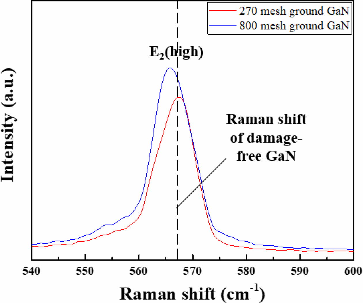
Fig. 5 compares the Raman measurements for GaN after the 270 and 800-mesh grinding. Of the Raman modes, the E2 (high) mode, a horizontal vibration mode, was used to gauge the residual stress in the GaN crystal [21, 22]. For stress-free bulk GaN, the Raman shift of the E2 (high) peak is located at approximately 567.2 cm-1. Based on this, the material with compressive or tensile stress shows a higher or lower peak position, respectively [23-25]. Using the 270-mesh grinding wheel, sample A exhibited a 567.5 cm-1 shift position, a position higher than the theoretical value, indicating that the compressive stress was subject to the sample. At the 800-mesh grinding, the sample has a value of 565.8 cm-1, and the E2 (high) peak is shifted to the left, meaning that tensile stress exists in the material. This result is in good agreement with the results shown in Fig. 4.
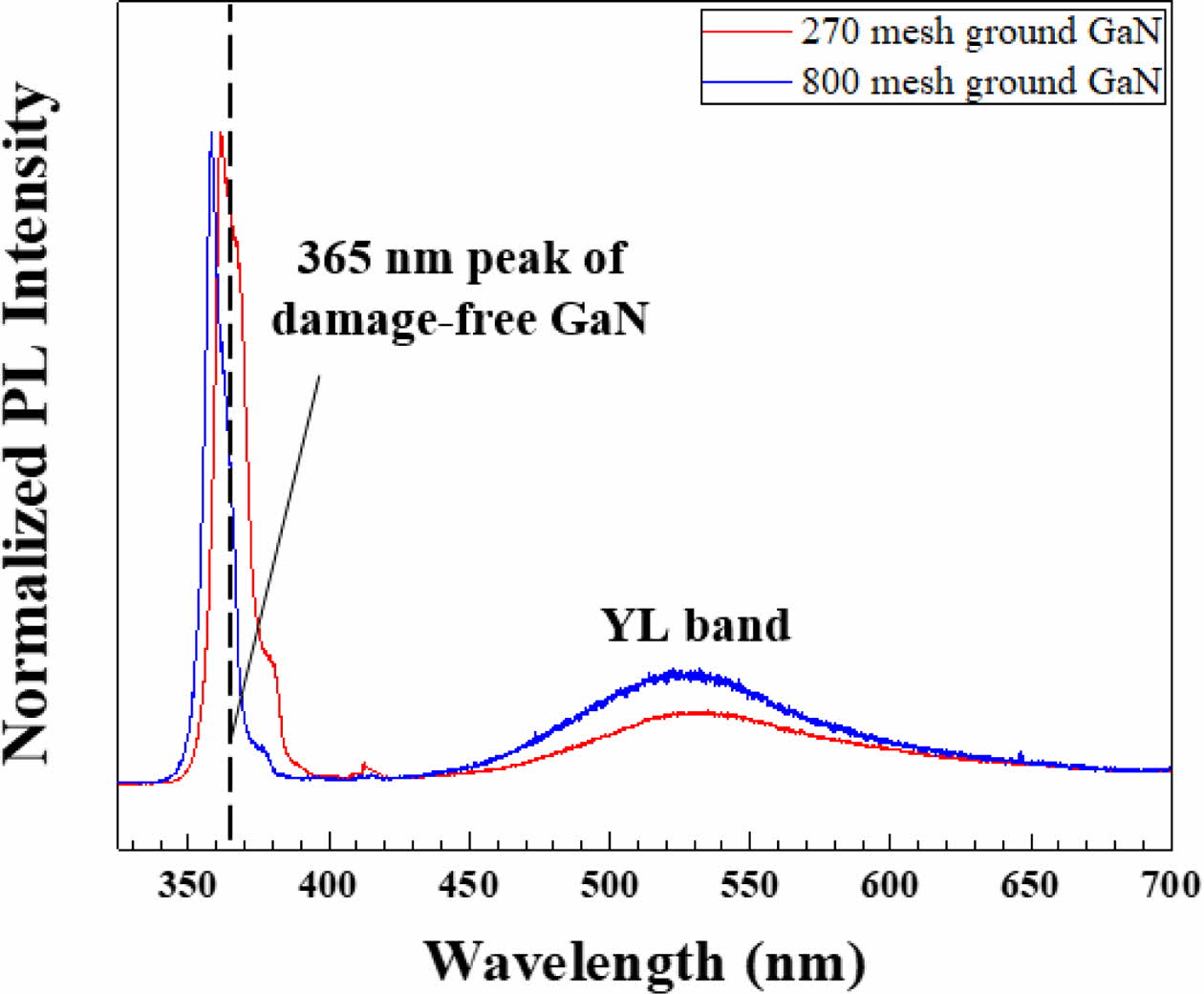
Fig. 6 is a graph comparing PL measurements for GaN after the 270 and 800-mesh grinding. In the normalized PL data on the main peak of 365 nm, it can be seen that the intensity of the peak in the yellow luminescence (YL) region of the 800-mesh is higher than that of 270-mesh. GaN theoretically absorbs UV rays in the 325 nm region and mainly emits light in the 365 nm UV region corresponding to the 3.4 eV bandgap. However, when defects such as impurities and vacancies exist within the material, trap levels in the bandgap are formed, and the YL phenomenon, which means that light in the visible ray region emits, occurs [26-28]. The YL intensity ratio value of the 800-mesh sample is higher than that of the 270-mesh because the number of trap states in the bandgap increases as a result of the increase in defects inside the GaN [29]. The increase in the YL intensity ratio of sample B with a thin SSD layer suggested that the inhibition of the exciton recombination mechanism was affected not only by the depth of the SSD but also by the density of the SSD. In addition, the main peak (365 nm) shifted to the lower wavelength—361.5 nm and 358.2 nm at samples A and B, respectively—which is called the blue shift. The blue shift indicates an increase in the bandgap energy. Considering that the bandgap energy was inversely proportional to the interatomic distance, it was demonstrated that compressive stress existed in the samples and in particular, greater com- pressive stress was applied to sample B [30]. It can be observed that the results of the above PL are contrary to the previous XRC and Raman results. This was considered to be related to the range of measurement of the specimen according to each analysis device.
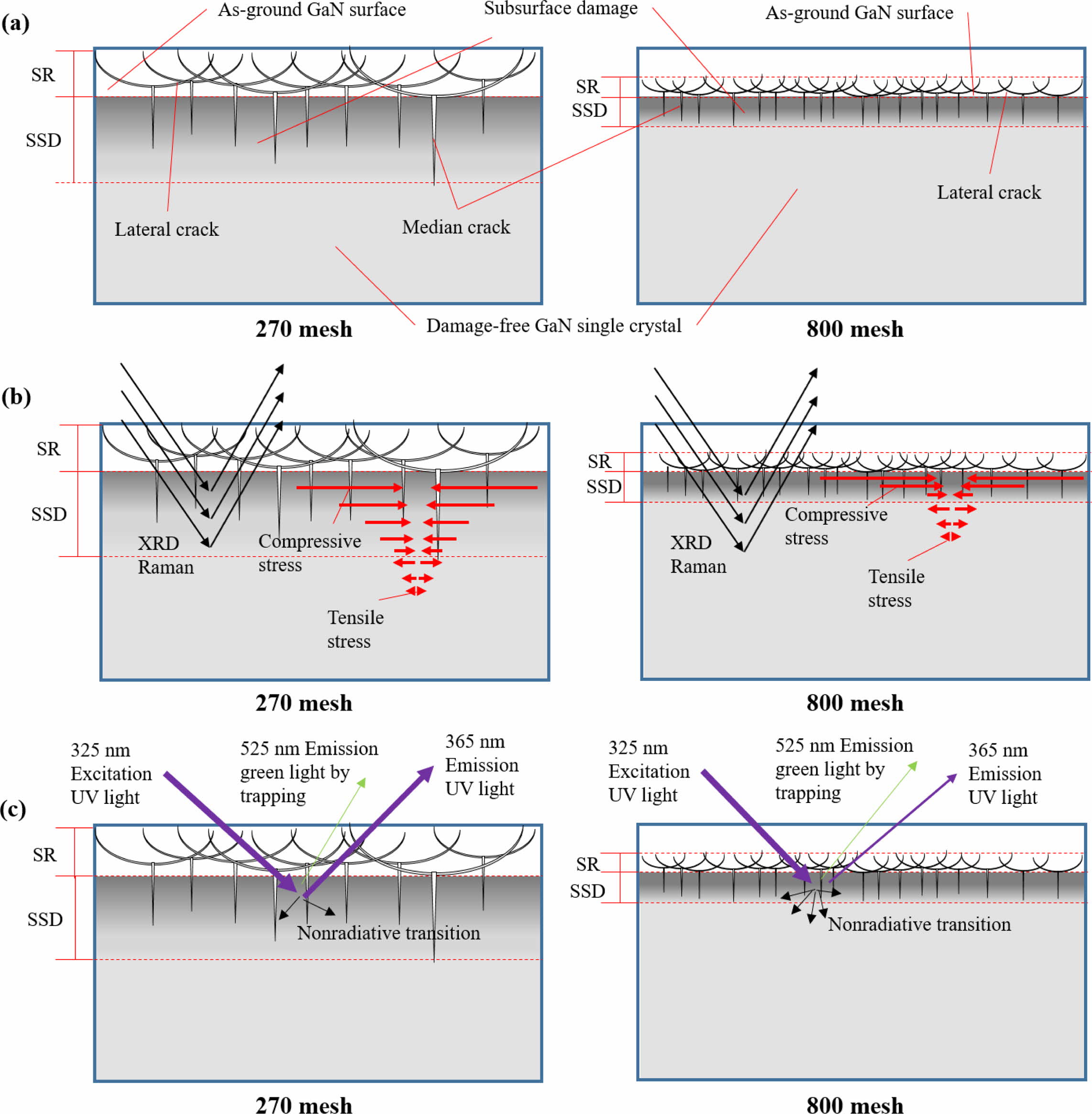
Fig. 7 shows a schematic diagram of the analysis range of the SSD generated after grinding and the analysis devices used. Fig. 7(a) is a cross-sectional schematic diagram of the ground GaN single crystal, and Fig. 7(b) and (c) illustrate the mechanisms of measuring the XRC, Raman, and PL data. For brittle materials such as GaN, plastic deformation occurs in a certain area between the abrasive grit and the GaN substrate because a strong force is applied by the abrasive of the grinding wheel [31]. The area over which this stress is directly applied is called the plastic zone, and median and lateral cracks in the vertical and horizontal directions to the GaN, respectively, occur around the plastic zone, causing potential chipping [32, 33]. When these lateral and median cracks accumulate, SR and SSD are formed correspondingly, and it can be seen that the depth of both SR and SSD decreases at a larger mesh size according to previous results [33, 34]. For the finer grit grinding wheel, the contact area between the GaN surface and the grinding wheel abrasives becomes relatively larger than that of the coarser grit grinding wheel because of the smaller abrasive size of the grinding wheel. Owing to these mechanisms, the density of damage per unit area of GaN increased with finer grinding wheels [35]. In the case of XRC and Raman, it is judged that tensile stress is predominantly observed because light penetrates deeper areas than PL. After all, it can penetrate up to 5-6 µm and includes information on the undamaged areas of the deep area [20, 36]. However, PL has a low penetration depth of 100-200 nm in GaN and reflects only the properties near the surface. Therefore, the data for sample B indicated that the compressive stress was intensified, the number of defects increased, and the luminous properties were reduced [37]. In other words, it can be interpreted that the coarse grinding wheel causes an increase in the SR and the depth of SSD; however, the fine grinding wheel causes the depth of SSD to decrease while the defect density increases. Too coarse grinding wheels induce deep SR and SSD, which must be removed during polishing. In contrast, for an extremely fine grinding wheel, the material cannot accept the whole yield stress and plastic deformation owing to the excessive increase in the density of the SSD, and the probability of forming macro-cracks in the wafer increases [38, 39]. Accordingly, it is necessary to select an appropriate grinding wheel for GaN in consideration of the mechanism according to the abrasive size of the grinding wheel, and it is believed that the appropriate selection of the abrasive size of the grinding wheel will act as a key factor to improve the GaN wafer manufacturing yield.
|
Fig. 1 Schematic representation of grinding wheel and the WLI, SEM images of GaN after grinding by (a) 270-mesh and (b) 800-mesh grinding wheels. |
|
Fig. 2 OM images according to GaN polishing time until 120 min after grinding with abrasive grit sizes of (a) 270-mesh and (b) 800-mesh. |
|
Fig. 3 STEM images of GaN cross-sectional plane by grinding with abrasive grit sizes of (a) 270-mesh and (b) 800-mesh. |
|
Fig. 4 XRC spectra for GaN sample after 270 and 800-mesh grinding. |
|
Fig. 5 Raman spectra for GaN sample after 270 and 800-mesh grinding. |
|
Fig. 6 Normalized PL spectra for GaN sample after 270 and 800- mesh grinding at room temperature. |
|
Fig. 7 Schematic diagram of (a) GaN internal defect distribution and (b) XRC and Raman, (c) PL application according to grinding wheel mesh. |
The bulk GaN single crystal grown by the HVPE method was ground with a diamond grinding wheel of 270 and 800-mesh sizes, and the optical properties were analyzed to control the defects caused by grinding. By measuring the morphology and SR of the ground GaN using WLI and SEM, it was found that high-mesh grinding had a lower SR. The polishing time was reduced with a finer grit size of the grinding wheel during the mechanical polishing process. Through STEM, it was possible to measure the distribution of the SSD inside GaN, and it was found that deeper damage was left at a lower-mesh grinding wheel. It could be seen that the XRC showed compressive stress in the smaller mesh, tensile stress in the larger mesh, and crystallinity was higher in the larger mesh. The Raman spectra also showed compressive stress in a low mesh and tensile stress in a high mesh, similar to the XRC results. In the PL data normalized to the 365 nm main peak, however, it was found that the YL characteristics were higher at the high mesh, and many defects were concentrated near the surface through the blue shift. Based on the above results, because the measurement range was different depending on the analytical equipment, it was inferred that XRC and Raman measured a deeper area, and PL measured a shallower area. It could be inferred that the lower the mesh of the grinding wheel, the deeper the SR and SSD generated, but the higher the mesh, the higher the density of SSD near the surface. It is possible to control the depth and density of the SR and SSD using the appropriate grit size of the grinding wheel. Therefore, when planarization is performed through appropriate mesh grinding in the future, the depth and density of the SSD for GaN can be appro- priately adjusted to affect the control of the subsequent polishing process so that defects caused by grinding can be effectively controlled. It is believed that an efficient improvement of the GaN wafering process can be achieved. Therefore, a continuous grinding process according to the combination of the grinding wheels of the smaller or larger mesh is considered necessary.
This work was supported by the Industrial Strategic Technology Development program funded by the Ministry of Trade Industry & Energy of KOREA (Project No. 10080599).
- 1. H.P. Maruska, and J.J. Tietjen, Appl. Phys. Lett. 15 (1969) 327-329.
-

- 2. A.S. Augustine Fletcher, and D. Nirmal, Superlattices Microstruct. 109 (2017) 519-537.
-
- 3. E. Gu, C.W. Jeon, H.W. Choi, G. Rice, M.D. Dawson, E.K. Illy, and M.R.H. Knowles, Thin Solid Films 453-454 (2004) 462-466.
-
- 4. F.K. Yam, L.L. Low, S.A. Oh, and Z. Hassan, in "Gallium nitride: an overview of structural defects" (InTech, 2011) p. 99-136.
-
- 5. J. D.D. Manchon, J. A.S. Barker, P.J. Dean, and R.B. Zetterstrom, Solid State Commun. 8 (1970) 1227-1231.
-
- 6. H. Aida, H. Takeda, S.W. Kim, N. Aota, K. Koyama, T. Yamazaki, and T. Doi, Appl. Surf. Sci. 292 (2014) 531-536.
-
- 7. L. Zhang, and H. Deng, Appl. Surf. Sci. 514 (2020) 145957.
-
- 8. H. Lee, H. Kasuga, H. Ohmori, H. Lee, and H. Jeong, J. Cryst. Growth 326 (2011) 140-146.
-
- 9. H. Aida, T. Doi, H. Takeda, H. Katakura, S.W. Kim, K. Koyama, T. Yamazaki, and M. Uneda, Curr. Appl. Phys. 12 (2012) S41-S46.
-
- 10. K.J. Kim, J.S. Jeong, H.J. Jang, H.M. Shin, and H.D. Jeong, J. Korean Soc. Precis. Eng. 25 (2008) 32-37.
- 11. H. Aida, H. Takeda, K. Koyama, H. Katakura, K. Sunakawa, and T. Doi, J. Electrochem. Soc. 158 (2011) 1206-1212.
-
- 12. J. Murata, T. Okamoto, S. Sadakuni, A.N. Hattori, K. Yagi, Y. Sano, K. Arima, and K. Yamauchi, J. Electrochem. Soc. 159 (2012) 417-420.
-
- 13. H.A. Lee, J.H. Lee, S.H. Lee, H.S. Kang, S.K. Lee, N. Oh, W.I. Park, and J.H. Park, J. Ceram. Process. Res. 21 (2020) 609-614.
-
- 14. J.J. Kim, and J.K. Lee, J. Ceram. Process. Res. 21 (2020) s68-s73.
- 15. C. Sun, E. Müller, M. Meffert, and D. Gerthsen, Adv. Struct. Chem. Imaging 5 (2019).
-
- 16. D. Key, E. Letts, C.W. Tsou, M.H. Ji, M. Bakhtiary-Noodeh, T. Detchprohm, S.C. Shen, R. Dupuis, and T. Hashimoto, Materials 12 (2019) 1925.
-
- 17. J.H. Shim, J.S. Park, and J.G. Park, RSC Adv. 10 (2020) 21860-21866.
-
- 18. V.V. Voronenkov, Y.S. Lelikov, A.S. Zubrilov, Y.G. Shreter, and A.A. Leonidov, in 2019 IEEE Conference of Russian Young Researchers in Electrical and Electronic Engineering, January 2019, (IEEE, 2019) pp. 833-837.
-
- 19. M. Li, Y. Cheng, T. Yu, J. Wu, J. He, N. Liu, T. Han, and G. Zhang, Mater. Des. 180 (2019) 107985.
-
- 20. T.Y. Tang, W.Y. Shiao, C.H. Lin, K.C. Shen, J.J. Huang, S.Y. Ting, T.C. Liu, C.C. Yang, C.L. Yao, J.H. Yeh, T.C. Hsu, W.C. Chen, H.C. Hsu, and L.C. Chen, J. Appl. Phys. 105 (2009) 023501.
-
- 21. H. Harima, J. Phys.: Condens. Matter 14 (2002) R967-R993.
-
- 22. C. Röder, F. Lipski, F. Habel, G. Leibiger, M. Abendroth, C. Himcinschi, and J. Kortus, J. Phys. D: Appl. Phys. 46 (2013) 285302.
-
- 23. G. Nootz, A. Schulte, L. Chernyak, A. Osinsky, J. Jasinski, M. Benamara, and Z. Liliental-Weber, Appl. Phys. Lett. 80 (2002) 1355-1357.
-
- 24. J.H. Park, H.A. Lee, J.H. Lee, C.W. Park, J.H. Lee, H.S. Kang, H.M. Kim, S.H. Kang, S.Y. Bang, S.K. Lee, and K.B. Shim, J. Ceram. Process. Res. 18 (2017) 93-97.
- 25. J.H. Park, H.A. Lee, C.W. Park, H.S. Kang, J.H. Lee, J.H. In, S.K. Lee, and K.B. Shim, J. Ceram. Process. Res. 19 (2018) 439-443.
- 26. J. Neugebauer, and C.G.V.d. Walle, Appl. Phys. Lett. 69 (1996) 503-505.
-
- 27. D.M. Hofmann, D. Kovalev, G. Steude, B.K. Meyer, A. Hoffmann, L. Eckey, R. Heitz, T. Detchprom, H. Amano, and I. Akasaki, Phys. Rev. B 52 (1995) 16702-16706.
-
- 28. C. Jung, J. Hwang, G. Yoo, D. Min, Y. Ryu, S. Moon, M. Kim, K. Shim, and O. Nam, J. Ceram. Process. Res. 15 (2014) 120-124
- 29. S.O. Kucheyev, M. Toth, M. R. Phillips, J. S. Williams, C. Jagadish, and G. Li, J. Appl. Phys. 91 (2002) 5867-5874.
-
- 30. A. Watanabe, T. Takeuchi, K. Hirosawa, H. Amano, K. Hiramatsu, and I. Akasaki, J. Cryst. Growth 128 (1993) 391-396.
-
- 31. S. Malkin and T.W. Hwang, CIRP Ann. 45 (1996) 569-580.
-
- 32. Q. Jiang, L. Zhang, and C. Yang, Mater. Sci. Semicond. Process. 122 (2021) 105446.
-
- 33. A. Esmaeilzare, A. Rahimi, and S.M. Rezaei, Appl. Surf. Sci. 313 (2014) 67-75.
-
- 34. S. Li, Z. Wang, and Y. Wu, J. Mater. Process. Technol. 205 (2008) 34-41.
-
- 35. S.J. Eder, S. Leroch, P.G. Grützmacher, T. Spenger, and H. Heckes, Int. J. Mech. Sci. 194 (2021) 106186.
-
- 36. H.Y. Kim, J.A. Freitas jr., and J. Kim, EPL 96 (2011) 26004-p1.
-
- 37. M.A. Reshchikov, and H. Morkoç, J. Appl. Phys. 97 (2005) 5-19.
-
- 38. X. Zhang, C. Yang, Y. Zhang, A. Hu, M. Li, L. Gao, H. Ling, and T. Hang, Electron. Mater. Lett. 16 (2020) 355-362.
-
- 39. B. Zhang, and J. Yin, Int. J. Extreme Manuf. 1 (2019) 012007.
-
 This Article
-
2022; 23(4): 436-442
Published on Aug 31, 2022
- 10.36410/jcpr.2022.23.4.436
- Received on May 25, 2022
- Revised on Jul 13, 2022
- Accepted on Jul 27, 2022
Services
- Abstract
introduction
experiment
result and discussion
conclusion
- Acknowledgements
- References
- Full Text PDF
Shared
Correspondence to
- Jae Hwa Park
-
AMES Micron Co. Ltd., Gimpo 10124, Korea
Tel : +82-70-8220-3773 Fax: +82-31-992-2700 - E-mail: jhpark3809@gmail.com
Clean-Energy Research Institute(CRI), Hanyang University, 222, Wangsimni-ro, Seongdong-gu, Seoul, 04763, Korea
E-mail: jcpr@hanyang.ac.kr