


- Analysis of morphological and electrical properties of optoelectronic devices with trimethoxy(proply)silane
Myung-Gyun Baeka, Sang-Seok Yunb, Jin-Sa Kimc, and Hong-Gyu Parkd,e, Sang-Geon Parkf,*
a Department of Materials Science and Engineering, Changwon National University, Changwon 51140, Korea
b Department of Mechanical Convergence Engineering, Silla University, Busan 46958, Korea
c Department of Automation System Engineering, Chosun College of Science & Technology, Gwangju, 61453, Korea
d Department of Smart Manufacturing Engineering, Changwon National University, Changwon, 51140, Korea
e Department of Electrical, Electronic, Control Engineering, Changwon National University, Changwon, 51140, Korea
f Department of Mechatronics Convergence, Changwon National University, Changwon, 51140, KoreaThis article is an open access article distributed under the terms of the Creative Commons Attribution Non-Commercial License (http://creativecommons.org/licenses/by-nc/4.0) which permits unrestricted non-commercial use, distribution, and reproduction in any medium, provided the original work is properly cited.
In this study, we investigated the deposition of trimethoxy(propyl)silane as a self-assembled monolayer (SAM) on the surface of an indium tin oxide (ITO) substrate in organic light-emitting diodes (OLEDs) by examining the changes in surface characteristics of the modified substrate with variations in deposition time and temperature. The highest contact angle was obtained at 160 oC, and for each deposition time, the contact angles were 63o, 66o, 80o, 96o, 103o, 103o, 103o, and 104o, respectively, indicating the contact angle, and thus the hydrophobicity, increased with increasing deposition time and temperature. In addition, after 90 min of deposition, adequate SAM coverage was achieved on the ITO surface. When the coverage ratio was calculated, ≥ 99% coverage was obtained after 90 min of deposition at 160 oC. Atomic force microscopy of samples with SAM coverage obtained after 90 min at different deposition tem-peratures revealed improvement in the surface roughness of the fabricated samples. The work function, measured using a photoelectron spectrometer, demonstrated a characteristic increase with increasing temperature. Thus, SAM deposition can improve the ITO surface properties depending on the time and temperature of deposition
Keywords: Organic Light-Emitting Diodes, Self-assembled monolayers, Indium tin oxide, Hole-injection layer
Organic light-emitting diodes (OLEDs), invented by Dr. C.W. Tang in 1982, are characterized by high efficiency and low-voltage motion and are based on the outstanding luminescence quality possessed by organic semiconductors [1]. OLEDs are considered next-generation technologies to replace the conventional liq-uid crystal displays, owing to their high luminous efficiency and color gamut. In OLEDs, the charge inserted from both poles moves to the light-emitting layer and emits light after being excited, and improvement in performance is a major factor in the process of insertion and transport [2]. In particular, the drive voltage, luminescence efficiency, and lifetime of an OLED are directly related to its performance. Therefore, balanced carrier insertion and transport are among the most important features of OLEDs [3]. A transparent conductive film (TCF) is a thin film, characterized by transparency and conductivity, which is used in various electronic components, such as information displays and solar panels [4, 5]. TCFs are essential for the production of transistors. TCFs mainly comprise a transparent conductive oxide (TCO) film, indium tin oxide (ITO) film being the most frequently used TCO film. Because the ITO films exhibit high conductivity and permeability, they are frequently used in all types of display products, including OLEDs [6-9]. Well-known materials used for fabricating the hole injection layer include phthalocyanine, m-MTDATA, 2-TNATA, polyaniline, and oligothiophene. To achieve the out-standing characteristics of OLEDs, the highest occupied molecular orbital (HOMO) energy level of the injection layer should be only slightly different from that of the transport layer of the cathode and the work function. Materials that show such excellent properties and satisfy the conditions of the injection layer are required to enhance the performance of OLEDs [10-15]. Self-assembled monolayers (SAMs) are organic molecular films characterized by the regular supramolecular alignment of molecules on the film surface, which can improve the efficiency of hole-injection layers. The structure of SAMs can be divided into three parts: a head group that binds to the surface, an alkyl chain that forms a regular molecular film, and a functional group that defines the function of the molecular film [16]. SAMs are also capable of lowering the surface energy by reducing the hydroxyl groups on the surface [17]. While ITO provides a hydrophilic inorganic surface, the hole transport layer is composed of a hydrophobic organic material. This difference leads to heterogeneity between the two interfaces, with a consequent negative impact on the stability of the organic film [18]. Many researchers have reported that the work function between ITO and the hole transport layer can be controlled to lower the energy barrier between ITO and the organic material, thereby facilitating the injection of holes to enhance the luminescence efficiency and reduce the drive voltage [19, 20]. This study aims to improve the hole injection barrier between ITO and the hole transport layer. To achieve this goal, the temperature and time for the deposition of tri-methoxy(propyl)silane, a type of SAM, on the surface of ITO were varied, and the surface characteristics were investigated.
Test material
ITO shows ≥80% permeability at visible wavelengths, and owing to its low electric resistance and optical bandgap, ITO serves as one of the most useful materials [21]. In this study, ITO was purchased from AMG Co., South Korea, and was 15 mm in width and length, with a thickness of 1,500±100 Å = 150±10 nm, sheet resistance of ≤10 Ω/sq, and permeability of ≥85% at λ = 550 nm. For the fabrication of SAMs, trimethoxy (propyl)silane with purity > 98.0% and a methyl group (-CH3) was obtained from TCI.
Washing
The ITO substrate was ultrasonically cleaned using distilled water, acetone, distilled water, and isopropyl alcohol (IPA) in succession for 5 min each. The ITO substrate was dried on a hot plate at 150 oC for 10 min.
Methods
The vapor deposition method was used in this study. The cleaned ITO substrate and SAMs were placed in a 7 mL PFA container, which was positioned in a 500 mL PFA con-tainer and heated in an oven at 80, 120, or 160 oC for 1, 5, 10, 30, 60, 90, 120, and 150 min, inducing deposition of the evaporated SAMs on the surface of the ITO. The SAM-deposited ITO substrate was ultrasonically cleaned in IPA for 5 min and then adequately dried on a hot plate at 150 oC for 10 min. The transmittance of bare ITO and modified ITO with re-spect to temperature was compared using ultraviolet-visible (UV-visible) spectroscopy. Subsequently, contact angle measurements and atomic force microscopy (AFM) meas-urements were conducted to confirm the deposition of SAM on the ITO substrate. The per-formance was analyzed using the work function. The contact angle was measured using a GITsoft UNI-CAM. The AFM was performed using a Park Systems' XE-100 equipment, and the work function measurement was carried out using a FOCUS' HIS 13 UPS equip-ment.
In this study, SAM was used for the SAMs, and the effects of time and temperature on the level of deposition and performance were examined. The alkyl silane molecule was physically deposited on the surface of ITO via vapor deposition [22, 23]. The head group of the SAM is chemisorbed on the ITO surface, and as it is adsorbed over the entire surface of the substrate, a monolayer is formed. The alkyl chain ensures van der Waals interactions for the formation of an aligned monolayer. Lastly, the functional group can be varied according to the application requirements in different fields. In the present study, the functional group of SAM is a methyl group (-CH3). SAMs are formed by the adsorption of component molecules on the solid surface and simultaneous interactions among the molecules to create an assembly [24]. Water plays a critical role in the formation of SAM. Increasing the water content causes polymerization among the alkyl siloxane groups, which prevents the formation of SAMs. However, in the absence of water, incomplete assembly of the SAM results, highlighting the need for an adequate amount of water. Several studies have been conducted to investigate the role of water in the formation of SAMs. The results suggest that a layer of water is present on the hydrophilic surface of ITO and physisorption occurs on this layer. The van der Waals interactions among the alkyl chains of SAM lead to the surface adsorption of SAM on ITO, while a supramolecular assembly is created via simultaneous molecular interactions, thus allowing the surface properties to be adjusted [25, 26].
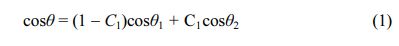
The transmittance results obtained via UV-visible spectroscopy are shown in Fig. 1. Wavelength mea- surements were carried out in the range of 300 to 800 nm, and the transmittance at 550 nm was 96.4% for ITO, 96.5% at 80 oC, 96% at 120 oC, and 96.3% at 160 oC. No significant differences were observed between the spectral peaks. These results show that when SAM is formed on an ITO substrate, there is no difference in transmittance, so it can be used as a hole injection layer.
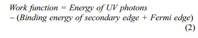
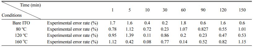
To verify whether the deposition of SAM on the ITO substrate was effective after vapor deposition, the contact angle was measured using a GITsoft UNI-CAM. The contact angles increased with an increase in the SAM deposition time. After 90 min, the contact angles remained constant at approximately 103o. This indicated that at 90 min, the SAM coverage was in a high-density stage on the ITO surface, and the van der Waals interactions of the SAM molecules led to uniform alignment, thus preventing any further change in the contact angle.
As shown in Fig. 2, increasing the deposition tem- perature led to an increase in the contact angle at the same deposition time, suggesting that the SAM-covered ITO surface acquired a high level of hydrophobicity as the deposition temperature increased. As the temperature increased and time passed, the SAM on the ITO substrate was well aligned by the van der Waals forces.
The contact angle can be quantitatively expressed based on the deposition ratio of SAM to ITO by applying Cassie’s Law and the following equation:
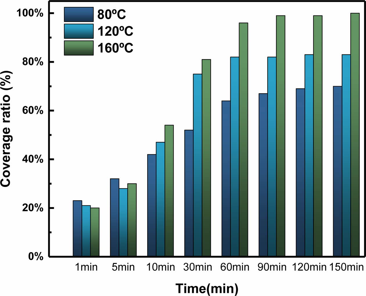
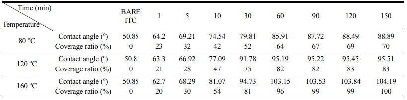
In the equation, C1 takes a value between 0 and 1, and by setting θ1 as the contact angle for bare ITO and θ2 as the contact angle after 150 min of deposition at 160 oC, the coverage ratio for the SAMs based on Cassie’s Law is as shown in Fig. 3. Detailed results are given in Table 1.
As shown in Fig. 3 and Table 2, for deposition times of 1-5 min, the coverage ratio on the ITO surface was least affected by the time and temperature, and after 10 min, a constant trend was observed. After 90 min, the measured contact angles at 80, 120, and 160 oC were approximately 88o, 95o, and 103o, respectively, indicating that the contact angle varied according to the temperature.
Based on Table 2, assuming that the SAM coverage ratio is 0% for bare ITO and 100% for ITO after 150 min of deposition, the coverage ratio was found to increase as the deposition time and temperature increased. At 160 oC, the temperature associated with the highest contact angle, the coverage ratio was ≥99%, compared to a contact angle of 103.53o after 90 min. This indicated the successful coverage of the ITO surface by SAM as well as the temperature dependence of the coverage ratio and hydrophobicity.
AFM measurements was conducted on films deposited on ITO substrate at different temperatures for a deposition time of 90 min, and the mean surface roughness was determined, where the contact angles exhibited a constant trend. The mean surface roughness (Rq) values at 80, 120, and 160 oC were 2.460, 1.768, and 1.551 nm, respectively. The Rq decreased as the deposition temperature increased, and the low Rq indicate a uniform SAM deposition on the ITO surface. This is confirmed by the observance of an elevated contact angle. The detailed AFM data are presented in Table 3.
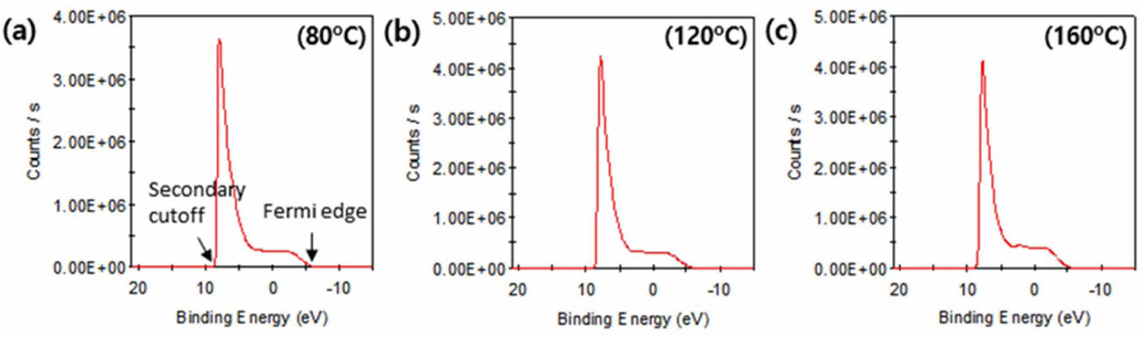
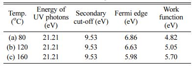
Fig. 4 shows the work function on the surface, as measured using a UPS device. The work function for ITO with SAM coverage at different temperatures (80, 120, and 160 oC) was calculated using the UV photon energy and the binding energy, according to the following equation [25]:
As shown in Table 4, an increase in temperature led to an increase in the work function. In general, ITO has a low work function of approximately 4-5 eV [26], while SAM deposition at varying temperatures lead to an increase in the work function. The calculated work functions at 80, 120, and 160 oC were 4.82, 5.05, and 5.70 eV, respectively, which indicated that the SAM coverage improved as the temperature increased. Thus, adjusting the temperature is likely to improve the efficiency of ITO coverage and hole transport layer.
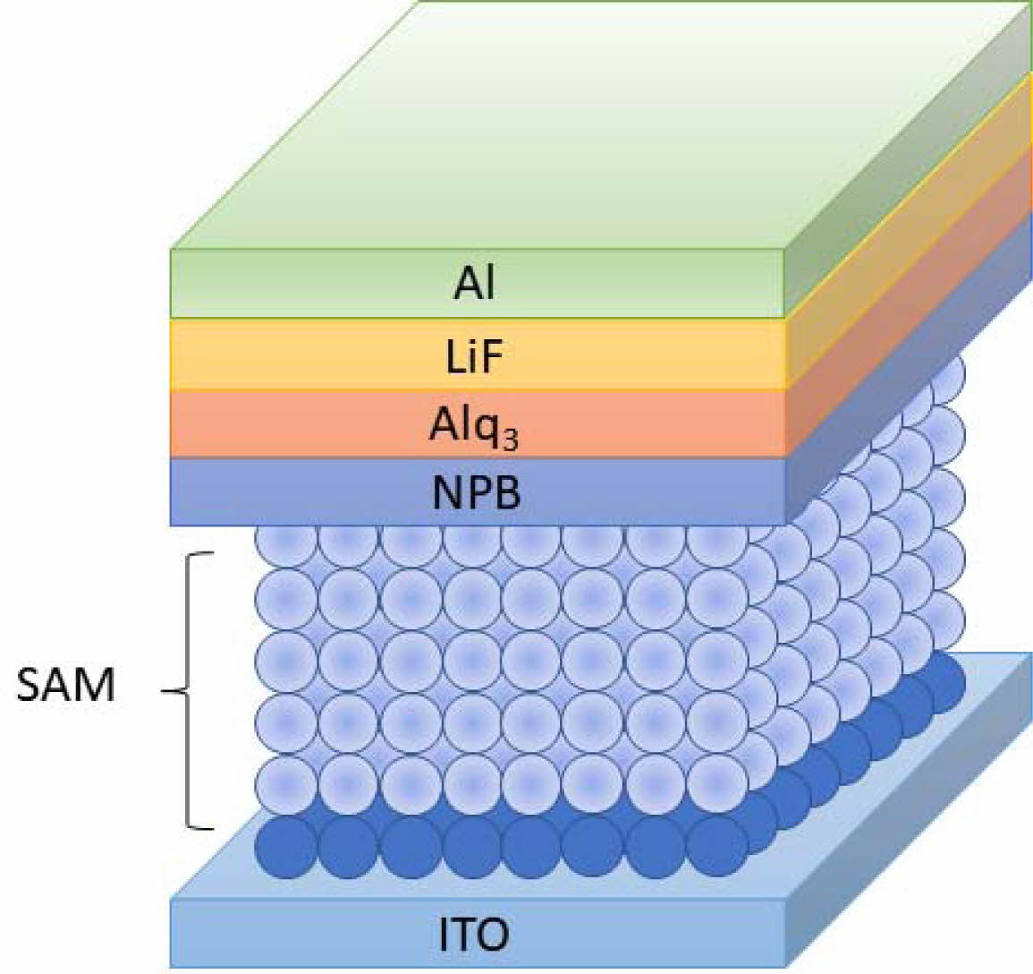
Fig. 5 shows OLEDs composed of ITO/SAM/NPB/Alq3/LiF/Al. OLEDs were fabricated to confirm electrical and optical characteristics when SAM was modified on ITO substrates.
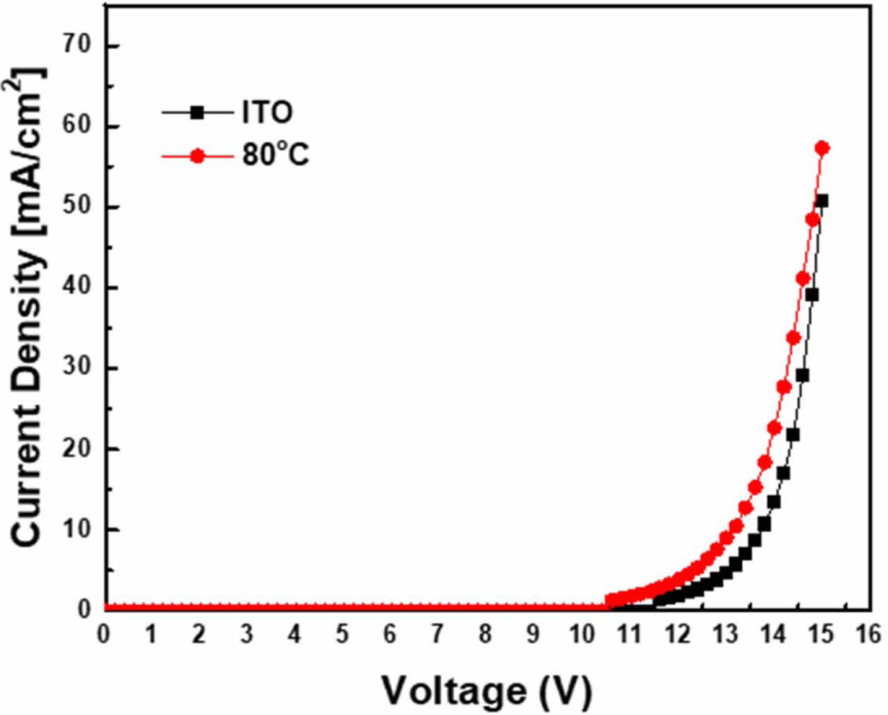
As shown in Fig. 6, the turn-on voltage of the device modified by SAM is lower than that of the unmodified device. When the current density of the device modified with SAM is 25 mA/cm2, voltage is approximately 13.5 V, whereas for the device without modification, at the same current, the voltage is approximately 14.5 V.
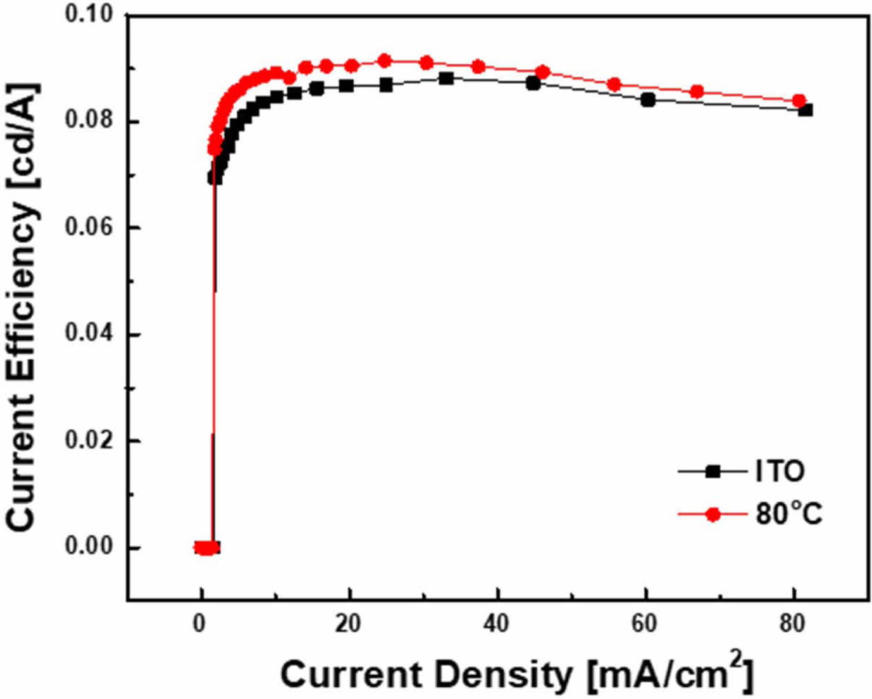
Fig. 7 shows the current efficiency of the fabricated samples. Maximum current efficiency was 0.09 cd/A when SAM was deposited on ITO substrate and it was 0.08 cd/A for Bare ITO. In other words, when the ITO substrate is modified with SAM, a high current efficiency is observed due to the improved efficiency of the hole injection layer.
|
Fig. 1 UV-visible spectra of as-prepared samples. |
|
Fig. 2 Variation of contact angles according to time and temperature. |
|
Fig. 3 Coverage ratio calculated using Cassie's Law |
|
Fig. 4 Work function at each temperature: (a) 80 oC, (b) 120 oC, and (c) 160 oC. |
|
Fig. 5 Device structure of the SAM-based OLEDs. |
|
Fig. 6 Voltage–current density curve. |
|
Fig. 7 Current density–current efficiency curve. |
|
Table 3 Mean surface roughness of ITO after 90 min of deposition at different temperatures |
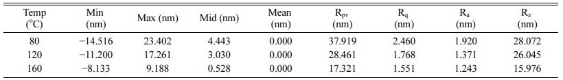
(Min - the smallest or lowest value in the line, max - the largest or highest value in the line, mid - the average of the min and max values, mean - the sum of the heights of all points in the line divided by the number of points, Rpv - the difference between min and max, Rq – R root mean square, Ra –R average, and Rz – ten point height) |
In this study, we investigated the influence of the time and temperature on the vapor deposition of the SAM on an ITO substrate. By comparing the transmittance of bare ITO with that of the SAM modified ITO substrate, it was demonstrated that there was no change in trans- mittance after the SAM deposition. The hole-transport layer mainly used a hydrophobic material. The contact angles increased steadily after 10 min of deposition, which suggested that the deposition of SAM increased the hydrophobicity of the ITO sur-face. The increase in hydrophobicity indicated that the SAM was well deposited on the ITO surface. The coverage ratio was quantified based on Cassie’s Law, and the results showed that the SAM coverage on the ITO surface was ≥99% after 90 min at 160 oC. The contact angles after 90 min were presumed to be identical based on a reliable alignment of SAMs through van der Waals interactions that were induced when the SAM deposition on the ITO surface reached a high-density stage at 160 oC. In addition, the AFM measure-ments showed that the mean surface roughness of ITO after 90 min of deposition, meas-ured as Rq, was 2.460 nm at 80 oC, 1.768 nm at 120 oC, and 1.551 nm at 160 oC, exhibiting a decreasing trend as the deposition time increased. The work function after 90 min of deposition was 4.82 eV at 80 oC, 5.05 eV at 120 oC, and 5.70 eV at 160 oC. The performance of the OLED was improved by reducing the turn-on voltage. The current efficiency of the ITO modified by SAM was superior to that of the bare ITO. These results indicated that as the time and temperature of the SAM deposition increased, the van der Waals interactions among the alkyl chains of SAM became adequate for a reliable SAM alignment on the ITO surface, suggesting an improvement in the ITO surface properties through SAM coverage. The surface roughness and hydrophobicity levels of ITO are critical in enhancing the efficiency of the ITO. Consequently, the deposition of SAM on the ITO surface was anticipated to enhance the efficiency due to the decreased injection barrier of the hole, thus contributing to the reduced drive voltage or improved power efficiency in OLEDs.
This research was supported by Changwon National University in 2021~2022.
- 1. C.-W. Tang, and S.A. VanSlyke, Appl. Phys. Lett. 51[12] (1987) 913-915.
-

- 2. I.-H. Park, I.-Y. Na, H. Joo, and G.-T. Kim, J. Semicond. Technol. Sci. 17[1] (2018) 50-53.
- 3. S.-Y. Park, D.-S. Kang, D.-W. Park, and Y.-S. Choe, Polymer Korea. 32[4] (2008) 372-376.
- 4. K.-H. Seo and K. -M. Lee, J. Ceram. Process. Res. 17[6] (2016) 564-568.
- 5. H.-K. Jeoung and K.-M. Lee, J. Ceram. Process. Res. 17[4] (2016) 281-285.
- 6. D.-C. Paine, T. Whitson, D. Janiac, R. Beresford, C.-O. Yang, and B. Lewis, J. Appl. Phys. 85[12] (1999) 8445-8450.
-
- 7. D.-A. Rider, R.-T. Tucker, B.-J. Worfolk, K.-M. Krause, A. Lalany, M.J. Brett, J.-M. Buriak, and K.-D. Harris, Nanotechnology. 22[8] (2011) 085706.
-
- 8. U. Betza, M.-K. Olsson, J. Marthy, M. Escolá, and F. Atamny, Surf. Coat. Technol. 200[20-21] (2006) 5751-5759.
-
- 9. V.-A. Dao, H. Choi, J. Heo, H. Park, K. Yoon, Y. Lee, Y. Kim, N. Lakshminarayan, and J. Yi, C. Appl. Phys. 10[3] (2010) S506-S509.
-
- 10. S.-A VanSlyke, C.-W. Tang, and L.-C Roberts, in “Electro- luminescent device with organic luminescent medium” (U.S. patent, 1999) p.1-16.
- 11. Y. Shirota, Y. Kuwabara, H. Inada, T. Wakimoto, H. Nakada, Y. Yonemoto, S. Kawami, and K. Imai, Appl. Phys. Lett. 65[7] (1994) 807-809.
-
- 12. K. Okumoto, and Y. Shirota, J. Lumin. 87 (2000) 1171-1173.
-
- 13. Y. Yang, and A.-J. Heeger, Appl. Phys. Lett. 64[10] (1994) 1245-1247.
-
- 14. C. Hosokawa, H. Higashi, and T. Kusumoto, Appl. Phys. Lett. 62[25] (1993) 3238-3240.
-
- 15. L. Fenenko, and C. Adachi, Thin Solid Films. 515[11] (2007) 4812-4818.
-
- 16. A. Ulman, in “An Introduction to Ultrathin Organic Films” (Langmuir, 2013) p.237-304.
-
- 17. Y. Zhao, L. Duan, D. Zhang, G. Dong, J. Qiao, L. Wang, and Y. Qiu, ACS Appl. Mater, Interfaces. 6[6] (2014) 4570-4577.
-
- 18. C.-L. Donley, D.-R. Dunphy, W.-J. Doherty, R. Zangmeister, A.-S. Drager, D.-F. O’Brien, S.-S. Saavedra, and N.-R. Armstrong, in “Indium tin oxide organic interfaces” (ACS, 2003) p. 133-153.
-
- 19. Y.-S. Chi, S.-M. Kang, and I.-S. Choi, Polym. Sci. Technol. 17[2] (2006) 172-181.
- 20. L. Yan, W.-TS Huck, and G.-M. Whitesides, J. Macromol. Sci. Part C. 44[2] (2004) 175-206.
-
- 21. M.-G. Baek, J.-E. Shin, D.-H. Hwang, S.-H. Kim, H.-G. Park, and S.-G. Park, Crystals. 10[8] (2020) 645.
-
- 22. G.-W. Choi, Y.-J. Seo, and W.-S. Lee, J. Korean Inst. Electr. Electron. Mater. Eng. 18 (2005) 354-355.
- 23. S.-R. Wasserman, Y.-T. Tao, and G.-M. Whitesides, Langmuir 5[4] (1989) 1074-1087.
-
- 24. M.-G. Baek, J.-E. Shin, and S.-G. Park, Crystals. 11[1] (2021) 26.
-
- 25. P. Silberzan, L. Leger, D. Ausserre, and J. Benattar, Langmuir. 7[8] (1991) 1647-1651.
-
- 26. Y.-S. Chi, S.-M. Kang, and I.-S. Choi, Polymer Science and Technology. 17[2] (2006) 172-181.
 This Article
-
2022; 23(3): 320-325
Published on Jun 30, 2022
- 10.36410/jcpr.2022.23.3.320
- Received on Dec 21, 2021
- Revised on Feb 21, 2022
- Accepted on Feb 22, 2022
Services
- Abstract
introduction
experimental procedure
results and discussion
conclusions
- Acknowledgements
- References
- Full Text PDF
Shared
Correspondence to
- Sang-Geon Park
-
Department of Mechatronics Convergence, Changwon National University, Changwon, 51140, Korea
Tel : +82-10-5954-8030 Fax: +82-55-213-3849 - E-mail: sgpark@changwon.ac.kr
Clean-Energy Research Institute(CRI), Hanyang University, 222, Wangsimni-ro, Seongdong-gu, Seoul, 04763, Korea
E-mail: jcpr@hanyang.ac.kr