


- Phase and electrical properties of Ca3Co4O9 ceramic prepared by a citrate sol-gel route
S D Yudantoa,*, S A Chandraa, R Robertoa, D P Utamaa, V O Herlinab and Lusianaa
aNational Research and Innovation Agency, Puspiptek, Banten, 15314, Indonesia
bUniversitas Teknologi Sumbawa, Nusa Tenggara Barat, 84371, IndonesiaThis article is an open access article distributed under the terms of the Creative Commons Attribution Non-Commercial License (http://creativecommons.org/licenses/by-nc/4.0) which permits unrestricted non-commercial use, distribution, and reproduction in any medium, provided the original work is properly cited.
Ca3Co4O9 is a ceramic material with the potential for application as a thermoelectric material. Several methods have been developed to manufacture the Ca3Co4O9 material. In this work, the Ca3Co4O9 ceramic was synthesized via citrate sol-gel route followed by mechanical milling. The samples after sintering at 850 oC for 3 and 6 hours were characterized for XRD studies. Based on XRD results, single phase of Ca3Co4O9 was shown in all samples. The crystallite size of Ca3Co4O9 samples in a range of 53.91-66.54 nm. The electrical measurement of Ca3Co4O9 sample showed an insulator phenomenon from 20 K to 80 K and a metallic behavior from 90 K to room temperature
Keywords: thermoelectric, sol-gel, electrical, insulator, metallic
Thermoelectric material could be a material which directly converts heat to electricity through the Seebeck effect. Several heat sources that can be utilized through thermoelectric materials include the manufacturing industry, transportations, and nuclear power plants. The performance of the thermoelectric is determined by the figure of merit (ZT) value of the material. ZT = Ѕ2T/κρ, where S is thermoelectric power or Seebeck coefficient (μV/K), T is the absolute temperature (K), κ is thermal conductivity (W/cm.K), and ρ is electrical resistivity (Ω·cm). For practical applications, the dimensionless ZT value must have a value higher than 1. The keys to increasing the ZT value of thermoelectric materials are high thermoelectric power, low electrical resistivity, and low thermal conductivity.
Ca3Co4O9 ceramic is a potential high-temperature thermoelectric material. In 2003, Shikano and Funahashi reported the ZT value of the single crystalline Ca3Co4O9 of 0.87 at 700 oC [1]. The Ca3Co4O9, a Co-based thermoelectric with the misfit-layered structure [Ca2CoO3]0.62CoO2, has several advantages including the absence of toxic materials, easy of manufacture, and high temperature stability [2]. Due to the misfit-layered structure, Ca3Co4O9 has a phenomenon that is correlated with an incommensurate spin-density-wave (IC-SDW) [3, 4]. This phenomenon is characterized by a change in the behavior of the metal to become an insulator when the temperature is cooled. Several studies report that IC-SDW phenomenon occurs at a temperature of around 80 K [3, 4].
Several fabrication methods have been developed in the manufacture of Ca3Co4O9 ceramics, including solid-state reaction [2, 4, 5], sol-gel [6-10], spark plasma sintering (SPS) [11-13], molten salt method [14], etc. From these various methods, the sol-gel method is proven to produce fine grains and high purity in the Ca3Co4O9 phase [6, 7, 9, 10]. Mohammed et al. synthesized Ca3Co4O9 using the starch-assisted sol-gel combustion method [7]. They investigated the influence of temperature and calcination time on the purity of the Ca3Co4O9 phase. They reported that a single phase of Ca3Co4O9 started to form at a calcination temperature of 800 oC with a dwelling time of 2 hours [7]. Bittner, et al synthesized Ca3Co4O9 using the sol-gel method. Using citric acid and EDTA for the complexing agent, the resulting gel was then calcined at 400 oC and 750 oC [6]. The calcined powder was then pelletized and sintered at 900 oC for 10 hours. They reported that the highest figure of merit (ZT) was 0.4 at 800 oC [6].
In this work, we report the synthesis and electrical properties of the Ca3Co4O9 ceramic using a sol-gel route followed by the mechanical milling. Our results indicate that the single phase of Ca3Co4O9 was formed for all samples. The evaluation of the IC-SDW phenomenon is discussed further in this report.
Materials preparation
In this work, the Ca3Co4O9 ceramics were prepared by using a citrate sol-gel route followed by the mechanical milling. Firstly, the analytical grade of Ca(NO3)2·4H2O and Co(NO3)2·6H2O powder was weighed and dissolved in the distilled water. The raw material solution was mixed with the citric acid solution was added to form a complex solution (light pink solution). To produce a gel (dark pink gel), the solution was heated on a hot-plate and stirred. The obtained gel was then dried at 120 oC for 6 hours to eliminate the moisture content. The result of the drying process was demonstrated by a color change from magenta to violet. The violet dry gel was ground and calcined at 500 oC and 800 oC. Secondly, the calcination powders were milled using a shaker mill for 1 and 2 hours. The fine powder was pressed into green pellets with a diameter of 10 mm and sintered at 850 oC for 3 and 6 hours in an air atmosphere. All samples were naturally cooled in the furnace. Table 1 provides a description of how the sample was prepared.
Material characterization
Ca3Co4O9 phase formation was identified using an X-ray diffractometer (XRD). The sintered sample was ground and characterized using Rigaku Smart Lab XRD measurements with Cu kα radiation sources (in the range of 2θ = 5-50 degrees at a rate of 0.01 degrees per step). A JEOL JSM-6390A scanning electron microscope (SEM) with the secondary electron (SE) at 20 kV was used to observe the fracture surface of the samples. The resistivity measurement was carried out using a teslatron cryogenic magnetometer with four-point probe (FPP) with no magnetic field at a temperature of 20-300 K.
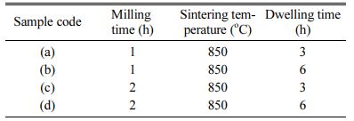
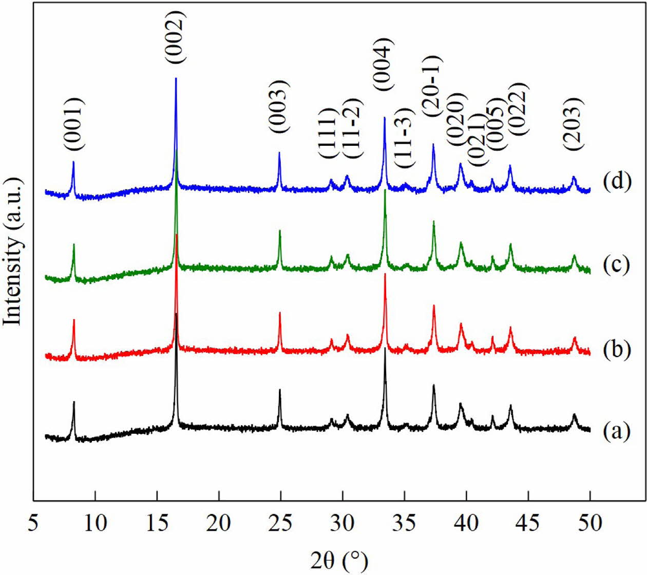
Fig. 1(a)-(d) show the diffraction pattern of the sintered Ca3Co4O9 samples at 850 oC for 3 and 6 hours. The diffraction peak at plane of (001), (002), (003), (111), (11-2), (004), (11-3), (20-1), (020), (021), (005), (022), and (203) are corresponding to the monoclinic crystal structure of Ca3Co4O9 phase. All peaks are have a good agreement with the standard diffraction pattern in previous reports [10, 15, 16]. The absence of an impurity phase in all four samples indicates that the samples synthesized by the sol-gel method have produced the Ca3Co4O9 single phase.
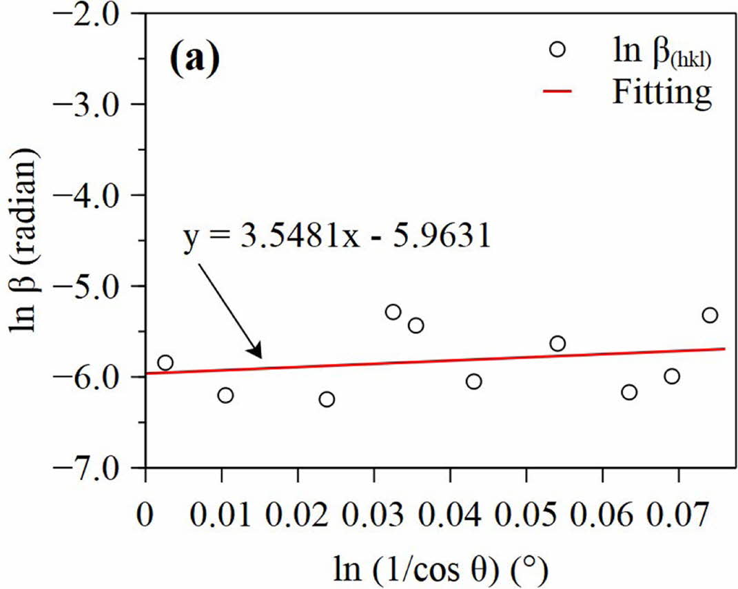
From the diffraction pattern, we can calculate the crystallite size of the Ca3Co4O9 samples through the modified Scherrer equation [17, 18]. The Scherrer equation is given in Eq. (1).
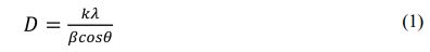
where D is the crystal size (nm), k is the shape factor (0.9), λ is the wavelength of the X-ray source (Cu kα = 0.15406 nm), β is the FWHM value (radian), and θ is the Bragg angle (°). Furthermore, the Eq. (1) can be written as Eq. (2).
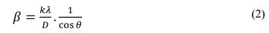
Based on Eq. (2), Monshi, et al modified the Scherrer formula that was then expressed in Eq. (3) [18].
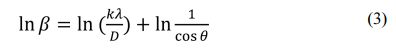
The plot of ln β versus ln (1/cos θ) is shown in Fig. 2. The linear fit of the data allowed to estimate the crystallite size of the sample from the intercept in Eq. (4). The intercept values of the four samples are -5.9361, -6.1736, -6.0669, and -6.0919, so that the estimated crystallite sizes of the sample (a), (b), (c), and (d) are 53.91 nm, 66.54 nm, 59.81 nm, and 61.30 nm, respectively. Based on the results of the calculation, it shows that the milling time does not really affect the crystallite size.
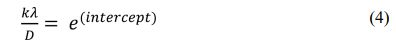
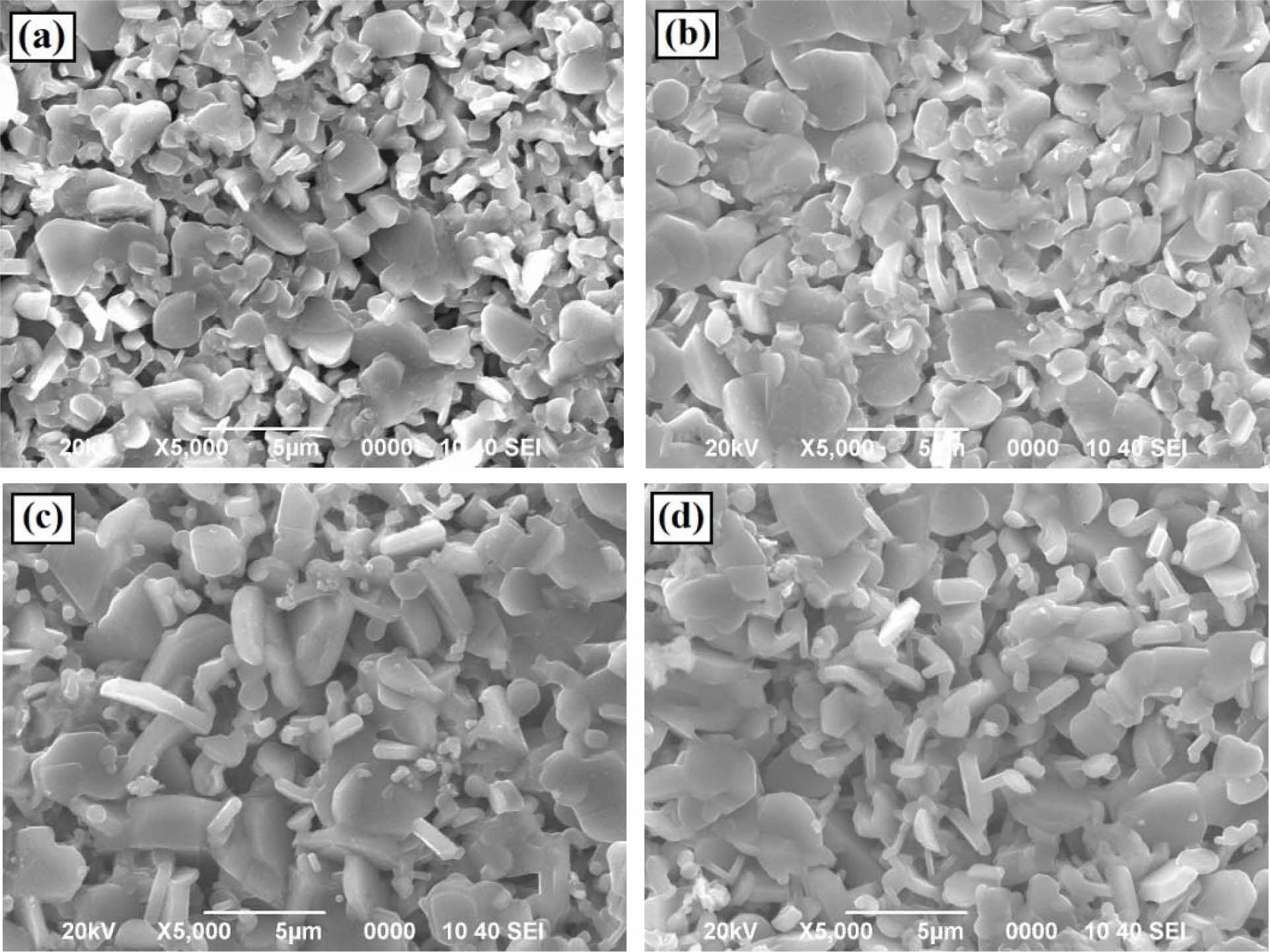
Fig. 3(a) - (d) show SEM images of fracture surface of the Ca3Co4O9 samples. The microstructural images of the four samples have a plate-like shape with various sizes. The SEM image shows that the grain size of the sample (a) is the smallest. As the dwelling time increases, the grain size increases in response to grain growth.
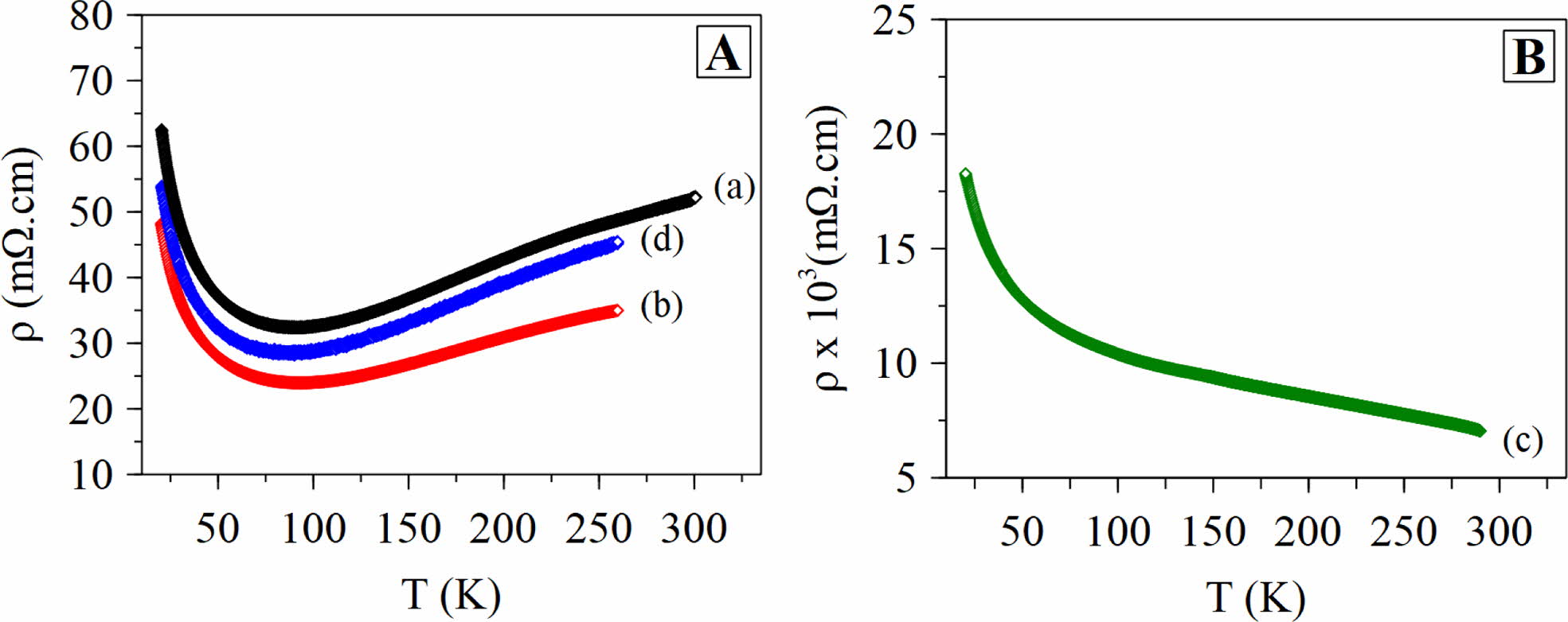
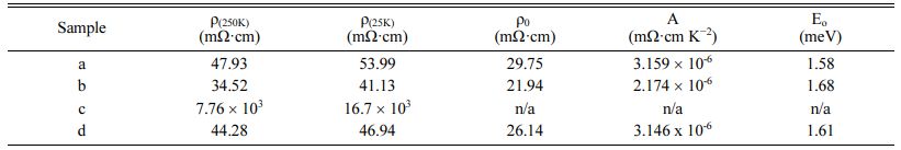
Fig. 4 shows the temperature dependence of the electrical resistivity of the sample (a) - (d). Measurements were performed in the temperature range from 20 K to 300 K. Due to the technical factor in the measurement process, the sample (b) and (d) was measured at a temperature from 20 K to 260 K. The plot of ρ vs T in the Fig. 4(a) indicates the phenomenon of metal-insulator (MI) for sample (a), (b), and (d). The resistivity value of the sample (a) was 47.93 mΩ·cm at 250 K and 32.41 mΩ·cm at a temperature of 95 K. With the increase in the sintering temperature, it can be seen in the ρ vs T plot that the resistivity value at 250 K of sample (b) decreased to 34.52 mΩ·cm. The decrease in the resistivity value is due to an increase in the density of the sample (b) as shown in Fig. 3 [4]. The increase in grain density in the sample (b) following the grain growth is the result of the dwelling time [5]. Meanwhile, a different phenomenon occurs in the sample (c), where the milling treatment for an hour and heating for 3 hours tend to have insulating properties as shown in Fig. 4(b). The phenomenon of an insulator with a resistivity value of 7.76 ´ 103 mΩ·cm at a temperature of 250 K shows similarities with the sample measured in the out-plane [19]. As reported by Masset, et.al, the electrical transport properties of the single crystalline Ca3Co4O9 have phenomena of an insulator and a metal-insulator [19]. It is interesting to explore further what the causes of the phenomenon of change of orientation from in-plane to out-plane.
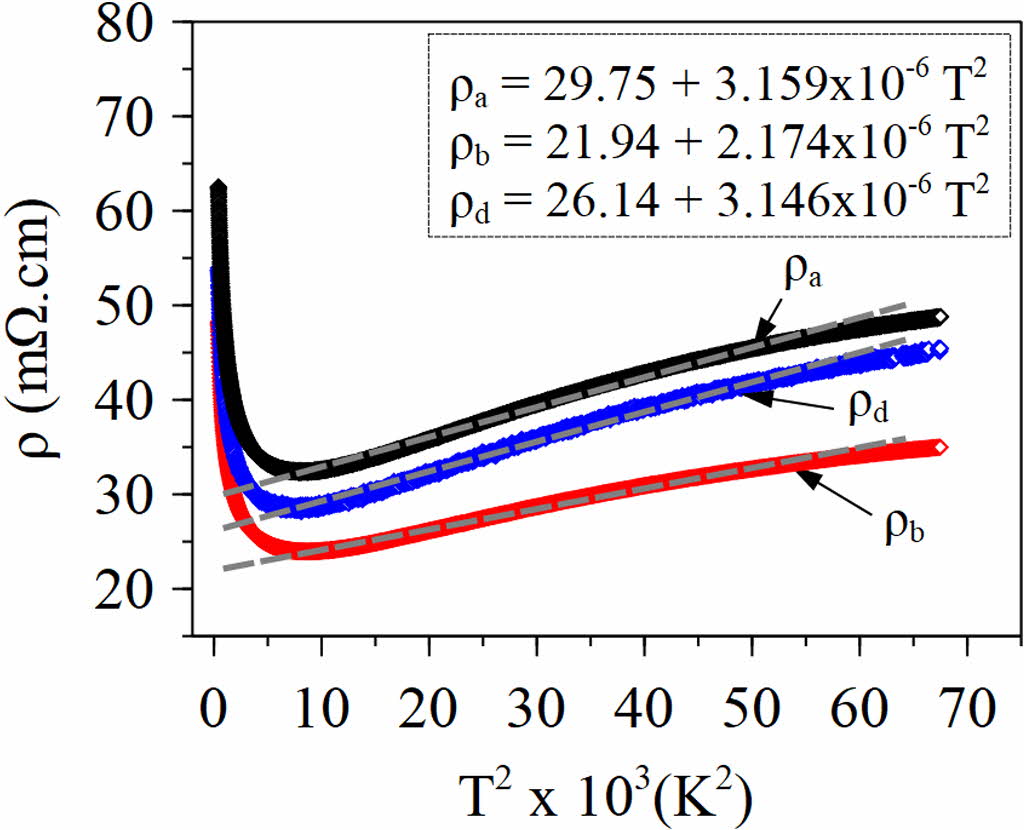
From the sample (a), (b), and (d), we observe an insulator phenomenon with a decrease in the resistivity value at a temperature of 20 K to 80 K. The resistivity value increases from 90 K to room temperature, indicating the metallic behavior. The metallic properties of the Ca3Co4O9 sample describe the behavior of the Fermi liquid [3, 4, 8]. From the value of ρ and T, then it is subsequently used to find the residual resistivity value by the Eq. (5) [4, 8].
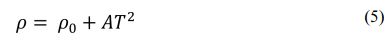
Where ρ is the resistivity value, ρ0 is the residual resistivity, A is the Fermi liquid transport coefficient, and T is the measurement temperature. The values of ρ0 and A are determined by fitting the ρ vs T2 curve. Fig. 5 shows the ρ versus T curve of the sample (a) and (d). The ρ0 and A values are presented in Table 2.
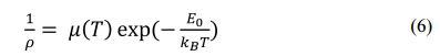
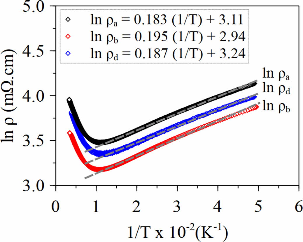
The transition from insulating to metal indicates that the Ca3Co4O9 sample is IC-SDW [3, 4]. Insulator behavior at low temperature variation of ρ with T of the Ca3Co4O9 obeys the thermally activated behavior described following Eq. (6) [3, 4].
To obtain the value of E0, then Eq. (6) is derived to Eq. (7). The plot of ln ρ versus 1/T is shown in Fig. 6.
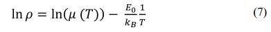
Where μ (T) is the mobility carrier, E0 is the energy gap caused by IC-SDW on the Fermi surface, and kB is the Boltzmann constant. From the linear fit to the data, we obtain the value of E0 for sample (a), (b), and (d). The E0 values of the sample (a), (b), and (d) obtained from Eq. (7) were 1.58 meV, 1.68 meV, and 1.61 meV, respectively.
|
Fig. 1 XRD pattern of Ca3Co4O9 samples. |
|
Fig. 2 Plot ln (1/cos θ) vs ln β with fitted lines of sample (a) |
|
Fig. 3 SEM images of Ca3Co4O9 samples sintered at 850 oC. (a). tmilling = 1 h, tsintering = 3 h, (b). tmilling = 1 h, tsintering = 6 h, (c). tmilling = 2 h, tsintering = 3 h, and (d). tmilling = 2 h, tsintering = 6 h. |
|
Fig. 4 Plot ρ vs T of Ca3Co4O9 samples. A) sample (a), (b), (d). B) sample (c). |
|
Fig. 5 Plot ρ vs T2 with fitted lines of sample (a), (b), and (d). |
|
Fig. 6 Plot ln ρ vs (1/T) with fitted lines of sample (a), (b), and (d). |
The Ca3Co4O9 ceramic has been successfully synthesized by using a citrate sol-gel route. Based on the XRD, all samples show a single-phase of Ca3Co4O9. The resistivity analysis of the samples showed that the insulator behavior was found at temperature from 20 K to 80 K and transformed into metal at temperature greater than 90 K. Based on IC-SDW, the energy gap values of the samples (a), (b), and (d) were 1.58 meV, 1.68 meV, and 1.61 meV, respectively.
The authors would like to thank the Research Center for Metallurgy and Materials for the support of the research facilities. This work was funded by the National Research and Innovation Agency of the Republic of Indonesia under the National Innovation System Research Incentive (INSINAS) grant (Contract Number: 12/INS-1/PPK/E4/2020).
- 1. M. Shikano and R. Funahashi, Appl. Phy. Lett. 82 (2003) 1851-1853.
-

- 2. Y. Miyazaki, Y. Suzuki, M. Onoda, Y. Ishii, Y. Morii, and T. Kajitani, Jap. J. Appl. Phy. 43 (2004) 6252-6258.
-
- 3. Y. Huang, B. Zhao, J. Fang, R. Ang, and Y. Sun, J. Appl. Phy. 110 (2011) 123713.
-
- 4. G. Kiirat, M.A. Aksan, S. Rasekh, M.A. Madre, J.C. Diez, and A. Sotelo, Ceram. Int. 41(2015) 12529-12534.
-
- 5. H. Amaveda, O.J. Dura, M. Mora, M.A. Torres, G. Guelou, M.A. Madre, S. Marinel, and A. Sotelo, Bol. Soc. Esp. Ceram. V. 60 (2021) 138-146.
-
- 6. M. Bittner, L. Helmich, F. Nietschke, B. Geppert, O. Oeckler, and A. Feldhoff, J. Eur. Ceram. Soc. 37 (2017) 3909-3915.
-
- 7. M.A. Mohammed, M.B. Uday, and S. Izman, J. Adv. Ceram. 9 (2020) 162-172.
-
- 8. B.C. Luo, J. Wang, M.M. Duan, K.X. Jin, and C.L. Chen, Materials Letters 120 (2014) 133-135.
-
- 9. Y.F. Zhang, J.X. Zhang, Q.M. Lu, and Q.Y. Zhang, Mat. Lett. 60 (2006) 2443-2446.
-
- 10. K. Agilandeswari and A. Ruban Kumar, J. Magn. Magn. Mater. 364 (2014) 117-124.
-
- 11. N. Wu, T.C. Holgate, N. Van Nong, N. Pryds, and S. Linderoth, J. Electron. Mater. 42 (2013) 2134-2142.
-
- 12. C.H. Lim, S.M. Choi, W.S. Seo, K.H. Kim, J.Y. Kim, and H.H. Park, J. Ceram. Process. Res. 13 (2012) 197-201.
- 13. Y. Liu, Y. Lin, Z. Shi, C.W. Nan, and Z. Shen, J. Am. Ceram. Soc. 88 (2005) 1337-1340.
-
- 14. N. Feng, Y. Jin, S. Guan, Y. He, L. Hao, and Y. Lu, J. Ceram. Process. Res. 17 (2016) 1541-1545.
- 15. P.R. Teja, A.R. Annamalai, G. Evangeline T.M. Srikanth, D.K. Agrawal, and C.P. Jen, Materials 14 (2021) 1-11.
-
- 16. T. Okuyama, T. Sugiyama, M. Tahashi, H. Goto, T. Natsume, and M. Takahashi, Electron. Comm. Jap. 102 (2019) 3-9.
-
- 17. M. Rabiei, A. Palevicius, A. Monshi, S. Nasiri, A. Vilkauskas, and G. Janusas, Nanomaterials 10 (2020) 1-21.
-
- 18. A. Monshi, M.R. Foroughi, and M.R. Monshi, World J. Nano Sci. Eng. 02 (2012) 154-160.
-
- 19. A. Masset, C. Michel, A. Maignan, M. Hervieu, O. Toulemonde, F. Studer, B. Raveau, and J. Hejtmanek, Phy. Rev. B 62 (2000) 166-175.
-
 This Article
-
2022; 23(3): 287-291
Published on Jun 30, 2022
- 10.36410/jcpr.2022.23.3.287
- Received on Oct 24, 2021
- Revised on Feb 3, 2022
- Accepted on Feb 10, 2022
Services
- Abstract
introduction
experimental methods
results and discussion
conclusions
- Acknowledgements
- References
- Full Text PDF
Shared
Correspondence to
- S D Yudanto
-
National Research and Innovation Agency, Puspiptek, Banten, 15314, Indonesia
Tel : +6281213024663 Fax: +62217560553 - E-mail: sigi012@brin.go.id
Clean-Energy Research Institute(CRI), Hanyang University, 222, Wangsimni-ro, Seongdong-gu, Seoul, 04763, Korea
E-mail: jcpr@hanyang.ac.kr