


- Structural and electrical properties of potassium tantalate niobate heterolayer thin films prepared by chemical solution deposition method
Byeong-Jun Parka,†, Sam-Haeng Leea,b,†, Myung-Gyu Leea,b, Joo-Seok Parkb, Byung-Cheul Kimc and Sung-Gap Leea,*
aDept. of Materials Engineering and Convergence Technology, RIGET, Gyeongsang National University, Jinju 52828, Korea
bBusiness Support Division, Korea Institute of Ceramic Engineering and Technology, Jinju 52851, Korea
cDept. of Convergence Electronic Engineering, Gyeongsang National University, Jinju 52828, KoreaThis article is an open access article distributed under the terms of the Creative Commons Attribution Non-Commercial License (http://creativecommons.org/licenses/by-nc/4.0) which permits unrestricted non-commercial use, distribution, and reproduction in any medium, provided the original work is properly cited.
In this study, K(Ta0.65Nb0.35)O3/K(Ta0.50Nb0.50)O3 heterolayer films were fabricated by the chemical solution deposition and spin-coating method and their structural and electrical properties were measured. All specimens represented a pseudo-cubic structure with a lattice constant of approximately 0.3999-0.4003 nm along with an observable K-deficient Ta2O5∙n(KTaO3) pyrochlore phase. Average thickness for a single coating was about 60~70 nm and average grain size was approximately 105-110 nm. Curie temperature was about 7oC and no dependence was observed on the number of coatings and sintering atmosphere. Remanent polarization of KTN heterolayer films decreased abruptly at about 50oC. The 6-coated KTN heterolayer film sintered in O2 atmosphere showed good ΔT of 1.93oC at about 60oC and ∆T/∆E of 0.15×10⁻⁶ KmV-1
Keywords: Potassium tantalate niobate, Heterolayer thin films, Electrocaloric effect, Hysteresis loop, Ferroelectric properties
The miniaturization and high-integration of electronic components is rapidly evolving due to the demand for quality performance and function in modern devices. However, the heating properties of these devices and their components are recognized as a serious problem area. Typical cooling techniques used in electronic com- ponents have refrigerant and thermoelectric effects [1, 2]. Concerning refrigerants, it is difficult to use them within small electronic devices due to environmental regulations. Whereas in the case of thermoelectric effects, they have low thermoelectric efficiency characteristics and are too expensive. In 2006, A. S. Mischenko et al. [3] reported a giant electrocaloric (EC) temperature change (ΔT ~ 12oC) in Pb(Zr0.95Ti0.05)O3 thin film at 220 oC, leading many researchers to conduct research on various EC materials [4, 5]. However, although Pb(Zr,Ti)O3 materials exhibit excellent ferroelectric properties, they also cause environmental problems due to their Pb elements and have limitations in their appli- cation in cooling devices operating at room tempera- ture due to their high Curie temperatures. Conversely, K(Ta1-xNbx)O3 materials have differences in their crystal structure and Curie temperature, due to the variation of the composition ratio of Ta and Nb, and are widely studied as an electro-optical material, ultra-high frequency material, and infrared detector material [6, 7].
Many researchers have studied the structural and electrical properties of KTN thin films according to manufacturing processes and substrates types, and compositions of KTN thin films [8-10]. However, there are few studies on the heterolayer thin films in which KTN thin films with different electrical properties and Ta/Nb composition ratios are alternately stacked. In this study, KTN heterolayer thin films were fabricated in which paraelectric K(Ta0.65Nb0.35)O3 and ferroelectric K(Ta0.50Nb0.50)O3 films with cubic and tetragonal crystal structures respectively, were alternately coated to control the Curie temperature near room temperature. Structural and electrical properties in relation to the number of coatings and sintering atmosphere were measured. Also, the applicability of the cooling material using EC was investigated.
KTN heterolayer thin films were fabricated using the chemical solution deposition method. KOC2H5, Ta(OC2H5)5, and Nb(OC2H5)5 were used as the starting materials and 2-Metoxyethanol as the solvent. All raw materials were weighed according to the composition formula of K(Ta0.65Nb0.35)O3 and K(Ta0.50Nb0.50)O3, and the synthesis process was carried out according to our previous experimental conditions [11]. On the Pt/Ti/SiO2/Si substrates, the first K(Ta0.65Nb0.35)O3 layer was spin coated at 2500 rpm and 30 sec, and pre-annealed at 400oC for 20 minutes to pyrolyze. Then, the second K(Ta0.50Nb0.50)O3 layer was spin-coated on the first layer with the same conditions. After repeating this process six times, KTN heterolayer films were annealed by insertion into a hot tube furnace and held at 750 oC for 1 hr under flowing oxygen. In addition, the 6-times coated KTN heterolayer films were sintered in both O2 and air atmosphere and the effects of the sintered atmosphere were measured. The structural properties of KTN heterolayer films were characterized by X-ray diffraction (XRD, D8, Bruker), field-emission scanning electron microscope (FE-SEM, Philips XL30S) and transmission electron microscope (TEM, JEM 2100F). For electrical properties, Pt top electrodes were deposited on the KTN heterolayer films by DC sputtering. The electrical properties of KTN heterolayer films were measured using an LCR meter (PM-6036, Fluke) and a ferroelectric tester (RT-66B, USA).
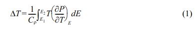
Fig. 1 shows the results of XRD patterns according to the number of coatings and the sintering atmosphere of KTN heterolayer films. As the number of coatings increases, crystallinity of KTN heterolayer films improved with increasing XRD peak intensities. All specimens represented a pseudo cubic structure with a lattice con- stant of approximately 0.3999-0.4003 nm. The K-defi- cient pyrochlore phase was observed near a diffraction angle of 2θ=28o. The pyrochlore phase formed at low sintering temperatures and gradually transformed into a pure perovskite phase within the 680-750oC range. No change in the crystalline properties of KTN films, which were sintered in O2 and air atmosphere, was observed since no oxygen nonstoichiometric phase was formed by evaporation of K ions at a low sintering temperature of 750oC [12].
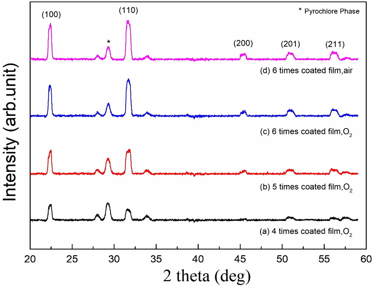
Fig. 2 shows surface and cross-sectional microstruc- tures according to the number of coatings and sintered atmosphere of KTN heterolayer films. All specimens showed dense and uniform grain structure with no pores. The average thickness for a single coating was about 60~70 nm. The dependence of the grain size on the number of coatings and sintering atmosphere was not observed. The average grain size was approxi- mately 105-110 nm.
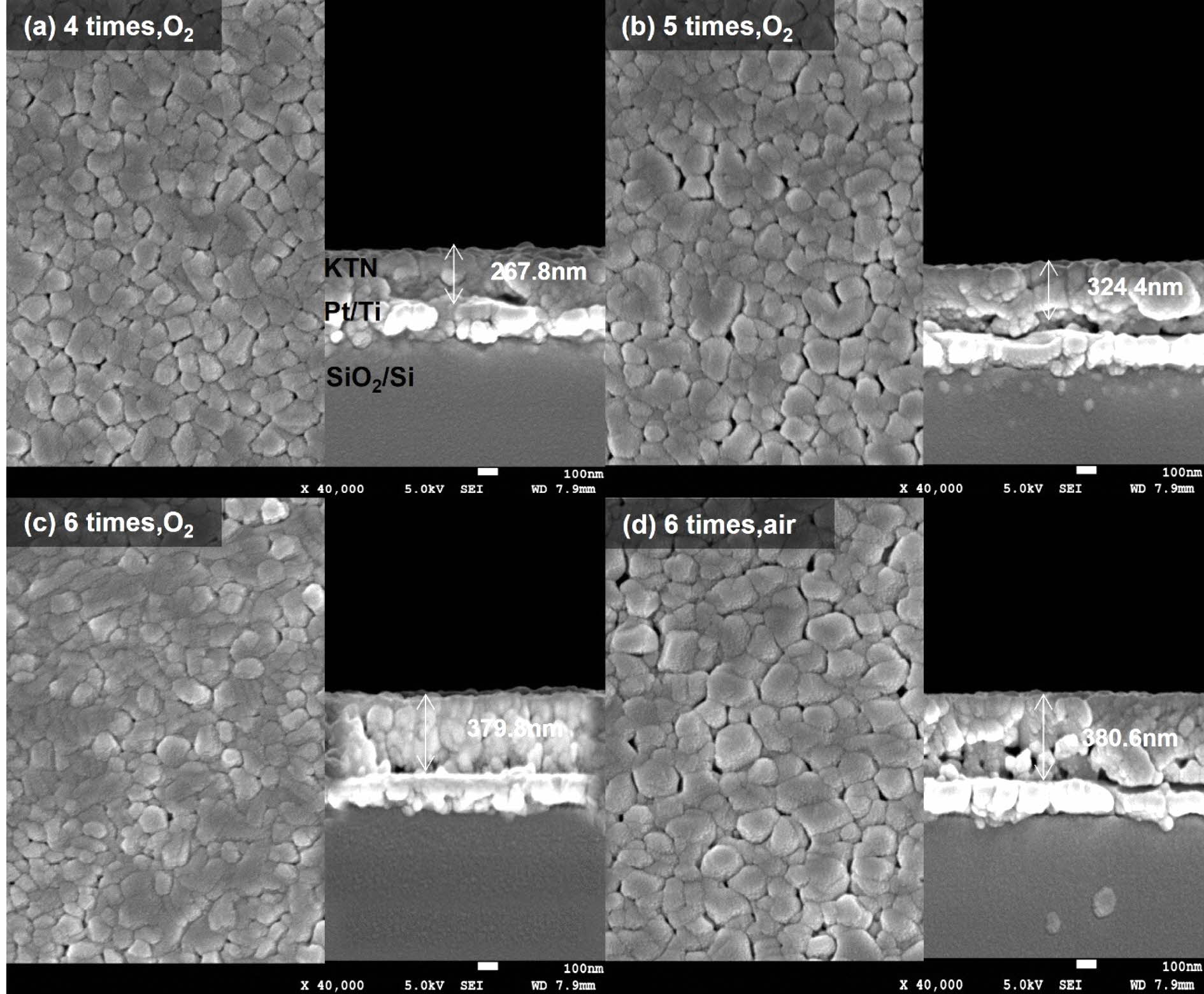
Fig. 3 shows (a) Cross-sectional TEM micrograph and (b) Energy dispersive X-ray spectroscopy (EDS) depth profile for the elements of the 6-coated KTN heterolayer film sintered in O2 atmosphere. Interface between K(Ta0.65Nb0.35)O3 layers and K(Ta0.50Nb0.50)O3 layers could not be observed. This is considered to be due to the same K, Nb, Ta constituent elements and the similar composition ratio. The partial bright and dark shades shown in Fig. 3(a) are thought to be due to the distribution of secondary phases with different crystal structures or compositions. As a result of the EDS analysis of Fig. 3(b), the dark area showed a low K and Nb ion intensity distribution. This is believed to be because of the K-deficient pyrochlore phase Ta2O5∙ n(KTaO3) (ASTM=12-29, 31-1098, 21-687), as shown in Fig. 1.
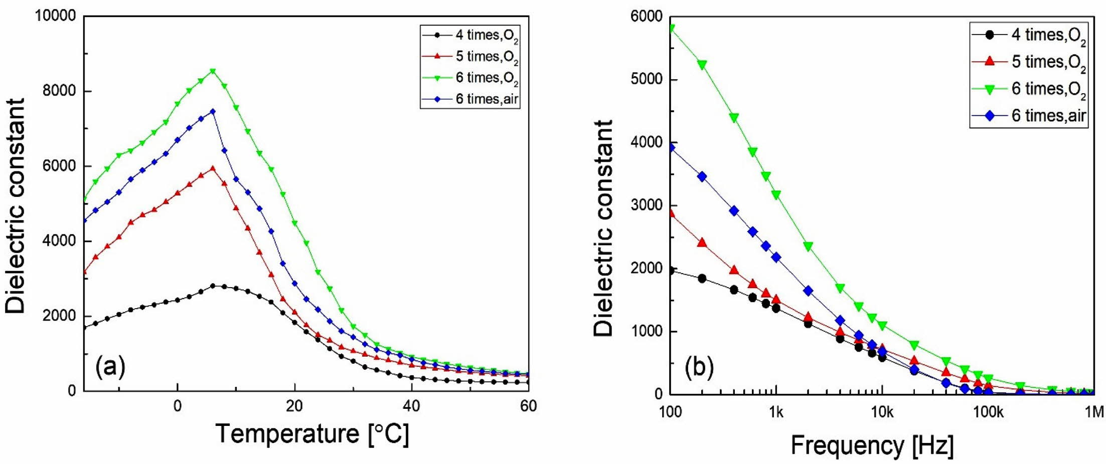
Fig. 4 shows the dielectric constant according to (a) temperature and (b) frequency of KTN heterolayer films. As the number of coatings, that is, the thickness of the specimen, increased, dielectric constant increased, which is thought to be due to the reduction in stress occurring at the interface between the film and the sub- strate. The phase transition temperature (Curie tem- perature, TC was about 7 oC, and no dependence on the number of coatings and the sintering atmosphere was observed. The gradual change in the dielectric constant according to the temperature is considered to be due to the diffused phase transition property of KTN hetero- layer films [13], and it showed a typical dielectric relaxa- tion property in which the dielectric constant decreases as the frequency increases. KTN heterolayer films sintered in O2 atmosphere showed slightly better dielectric constant properties than those sintered in air, which is thought to be due to the relatively dense grain structure, as shown in Fig. 2.
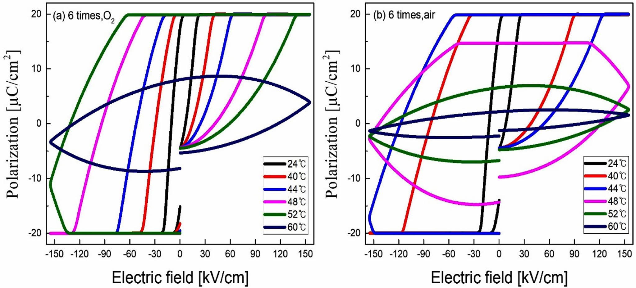
Fig. 5 shows the P-E hysteresis loops with variations of temperature of the 6-coated KTN heterolayer films. The remanent polarization of KTN heterolayer films sintered in O2 and air atmosphere abruptly decreased at 52 oC and 48 oC, respectively. In KTN heterolayer films with a Curie temperature of about 7 oC, the fact that ferroelectricity is maintained to about 50 oC is attributed to diffused phase transition characteristics caused by stress formed at the interface between K(Ta0.65Nb0.35)O3 layers and K(Ta0.50Nb0.50)O3 layers. In general, thin films are deposited on a substrate having different crystallo- graphic properties such as composition, unit cell struc- ture, or lattice constant etc. Particularly, ferroelectric thin films are deposited on a substrate with different structural characteristics, stress is generated at the inter- face due to a difference in crystallographic properties between the thin film and the substrate. This stress inhibits the rotation and/or switching of the dipole, and the Curie temperature tends to move toward the high temperature side [14, 15].
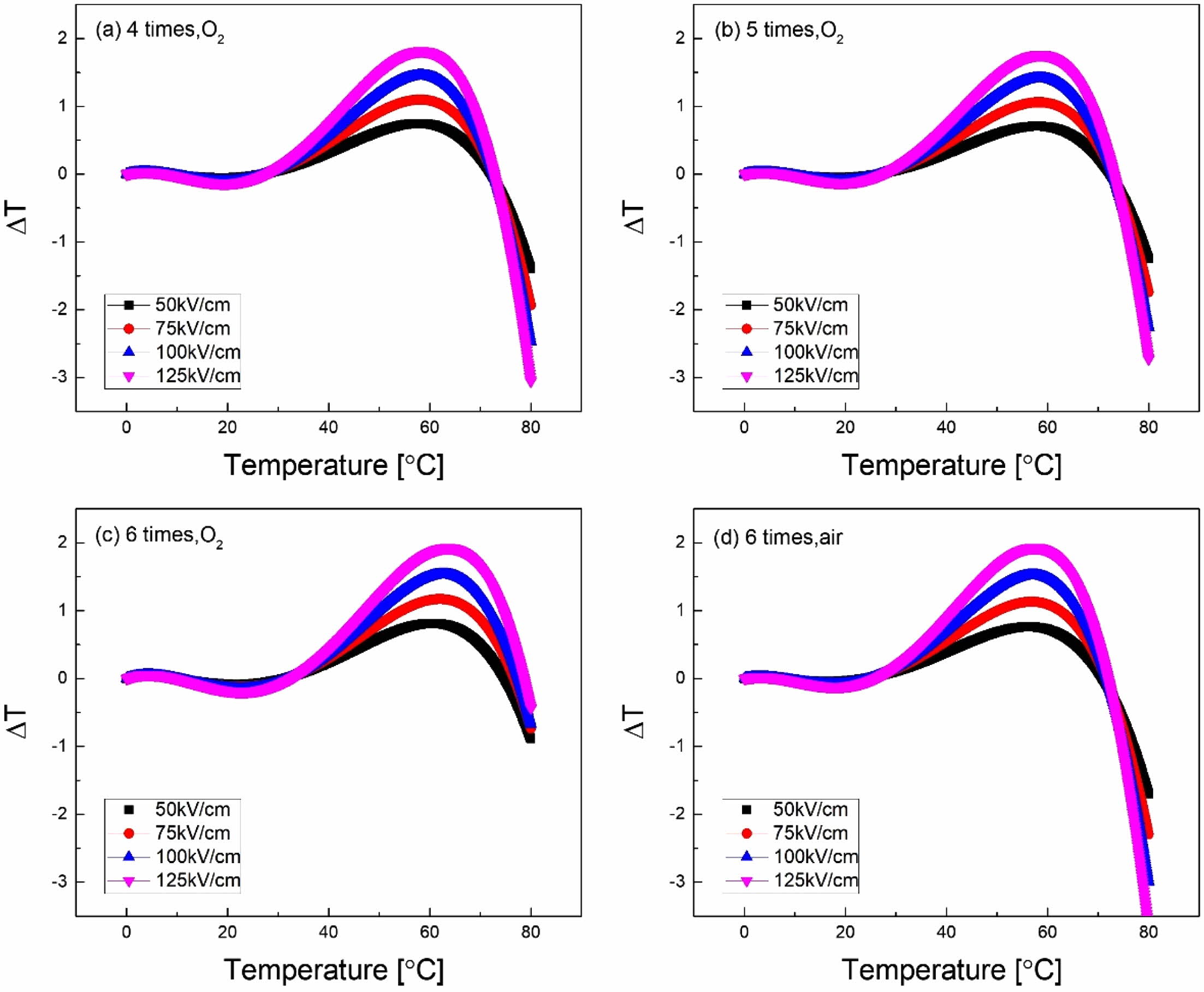
Fig. 6 shows the EC properties (ΔT) of KTN hetero- layer films according to temperature and ΔT was calculated from the following equation [16].
Here, C (=303.15 J/kg K) and ρ (=6.231 g/cm3) are the specific heat and density, respectively. No dependence on the EC properties of O2 and air sintering atmosphere was observed, and the 6-coated KTN heterolayer film sintered in O2 atmosphere showed the highest ΔT of 1.93 oC at about 60 oC. Also, EC efficiency (∆T/∆E), which represents the EC properties for the applied field, was 0.15×10⁻⁶ KmV-1. The values obtained in this study were slightly lower than 0.25×10⁻⁶ KmV-1 of Pb(Zr0.95Ti0.05)O3 film at 220 oC [3], but it has better properties than 0.13×10⁻⁶ KmV-1 [17] of PLZT ceramics and 0.02×10⁻⁶ KmV-1 [18] of BaTiO3 family multicap- acitor. From the experimental results of this study, it is expected that better EC properties can be obtained if homogeneous ferroelectric specimens are produced by changing sintering conditions to suppress the pyrochlore phase.
|
Fig. 1 XRD patterns according to the number of coatings and the sintering atmosphere of KTN heterolayer films. |
|
Fig. 2 Surface and cross-sectional microstructures according to the number of coatings and sintered atmosphere of KTN heterolayer films. |
|
Fig. 3 (a) Cross-sectional TEM micrograph and (b) Energy dispersive X-ray spectroscopy (EDS) depth profile for the elements of the 6- coated KTN heterolayer film sintered in O2 atmosphere. |
|
Fig. 4 Dielectric constant according to (a) temperature and (b) frequency of KTN heterolayer films. |
|
Fig. 5 P-E hysteresis loops with variations of temperature of the 6-coated KTN heterolayer films. |
|
Fig. 6 EC properties (ΔT) of KTN heterolayer films according to temperature. |
KTN heterolayer films were fabricated by alternately coating K(Ta0.65Nb0.35)O3 films and K(Ta0.50Nb0.50)O3 films. Structural and electrical properties were measured according to the number of coatings and the sintering atmosphere. All specimens represented a pseudo cubic structure and a K-deficient Ta2O5∙n(KTaO3) pyrochlore phase was also observed. In KTN heterolayer films with a Curie temperature of about 7 oC, the ferroelectricity was maintained at around 50 oC, which is believed to be due to strain formed at the interface between K(Ta0.65Nb0.35)O3 layers and K(Ta0.50Nb0.50)O3 layers. No significant dependence of structural and electrical properties on O2 and air sintering atmosphere has been observed. This is believed to be due to the low sintering temperatures. It is expected that better EC properties can be obtained if the formation of pyrochlore is suppressed by changing the sintering conditions of KTN heterolayer films.
This research was supported by Basic Science Research Program through the National Research Foundation of Korea (NRF) funded by the Ministry of Education (2020R1A6A1A03038697) and This work was supported by the National Research Foundation of Korea (NRF) grant funded by the Korea government (MSIT) (2021 R1I1A3052426)
- 1. J.H. Yoo, S.J. Cho, Trans. Electr. Electron. Mater. 20 (2019) 36-39.
-

- 2. S.P. Alpay, J. Mantese, S. Trolier-McKinstry, Q. Zhang, R.W. Whatmore, MRS Bull. 39 (2014) 1099-1111.
-
- 3. A.S. Mischenko, Q. Zhang, J.F. Scott, R.W. Whatmore, and N.D. Mathur, Science 311 (2006) 1270-1271.
-
- 4. X. Yan, M. Zhu, Q. Wei, S.-G. Lu, M. Zheng and Y. Hou, Scripta Materialia 162 (2019) 256-260.
-
- 5. M. Kwon, S. Lee, K. Kim, S. Choi, J. Ceram. Process. Res. 20 (2019) 395-400.
- 6. S. Guillemet-Fritsch, C. Chanel, J. Sarrias, S. Bayonne, A. Rousset, X. Alcobe, and M.L. Martinez Sarrion, Solid State Ionics 128 (2000) 233-242.
-
- 7. B. Liu, H. Zhang, Y. Zhang, X. Lv, Y. Yang, L. Wei, X. Wang, H. Yu, C. Zhang, and J. Li, Acta. Phys. Pol. A. 135 (2019) 396-400.
-
- 8. S.R. Sashital, S. Krishnakumar, S. Esener, Appl. Phys. Lett. 62 (1993) 2917-2919.
-
- 9. S. Wang, L. Wang, T. Zhou, T. Zhang, X. Xiong, A. Kugna, Ferroelectrics 186 (1996) 193-198.
-
- 10. A. Le Febvrier, S. Deputier, V. Bouquet, V. Demange, S. Ollivierr, A.C. Galca, C. Dragoi, R. Radu, L. Pintilie, M. Guilloux-Viry, Thin Solid Films 520 (2012) 4564-4567.
-
- 11. K.M. Kim, S.G. Lee, and M.S. Kwon, J. Ceram. Process. Res. 19 (2018) 302-305.
- 12. J. Mantese, A. Micheli, N. Schubring, A. Catalan, Y. Chen, R. Waldo, C. Wong, J. Appl. Phys. 72 (1992) 615-619.
-
- 13. C.C. Wang, M. He, F. Yang, J. Wen, G.Z. Liu, H.B. Lu, Appl. Phys. Lett. 90 (2007) 192904.
-
- 14. G.L. Brennecka, W. Huebner, B.A. Tuttle, P.G. Clem, J. Am. Ceram. Soc. 87 (2004) 1459-1465
-
- 15. M. Park, S. Lee, K. Kim and M. Kwon, J. Ceram. Process. Res. 18 (2017) 431-434
- 16. W. Geng, Y. Liu, X. Meng, L. Bellaiche, J. F. Scott, B. Dkhil, A. Jiang, Adv. Mater. 27 (2015) 3165-3169.
-
- 17. H. Maiwa, Jpn. J. Appl. Phys. 54 (2015) 10NB08.
-
- 18. S. Kar-Narayan, N. D. Mathur, J. Phys. D 43 (2010) 032002.
-
 This Article
-
2022; 23(3): 252-256
Published on Jun 30, 2022
- 10.36410/jcpr.2022.23.3.252
- Received on Jul 22, 2021
- Revised on Jan 18, 2022
- Accepted on Jan 25, 2022
Services
- Abstract
introduction
experimental
results and discussion
conclusion
- Acknowledgements
- References
- Full Text PDF
Shared
Correspondence to
- Sung-Gap Lee
-
Dept. of Materials Engineering and Convergence Technology, RIGET, Gyeongsang National University, Jinju 52828, Korea
Tel : +82-10-2686-4427 Fax: +82-55-772-1689 - E-mail: lsgap@gnu.ac.kr
Clean-Energy Research Institute(CRI), Hanyang University, 222, Wangsimni-ro, Seongdong-gu, Seoul, 04763, Korea
E-mail: jcpr@hanyang.ac.kr