


- Quenching effect of the exciton emission induced by an electric field in needle-like CdS rods
Hyeoncheol Kima, T.S. Jeonga,* and T. S. Kimb
aSemiconductor Physics Research Center (SPRC), School of Semiconductor and Chemical Engineering, Jeonbuk National University, Jeonju 54896, Korea
bDepartment of Physics, Jeonbuk National University, Jeonju 54896, KoreaThis article is an open access article distributed under the terms of the Creative Commons Attribution Non-Commercial License (http://creativecommons.org/licenses/by-nc/4.0) which permits unrestricted non-commercial use, distribution, and reproduction in any medium, provided the original work is properly cited.
In this paper, we studied the influence of electric fields on the exciton emissions of the needle-shaped CdS rod by using the combined photocurrent/photoluminescence (PC/PL) spectroscopies. We observed that the exciton emission strongly depended on the electric field while the defect-related emission weakly depended on the electric field. Intensity quenching and peak-shift effects of the exciton spectrum were observed as the electric field increased. To explain these effects, combined PC/PL measurements were introduced and they showed that excitons readily interact with the PC carriers of the photocreated electrons and holes. This interaction reduced the number of carriers participating in recombination, and the cause of the intensity decrease was attributed to the reduced recombination of free excitons. Thus, the shift of the exciton peaks was related to Stark effect induced by electric field. Consequently, we extracted out that exciton–electron scattering in emission spectra were the result of an interaction induced by the external electric field
Keywords: Electric field, Exciton-electron scattering, Stark effect
Binary or ternary alloyed semiconductor of Cd materials combined with S, Se, and Te components has been extensively investigated. Among these compounds, ternary cadmium chalcogenides of CdSeScan be varied from visible (2.42 eV for CdS) to near IR (1.73 eV for CdSe) by changing the element rate leading to a decrease in the bandgap energy by increasing the Se content [1-4]. Especially, the binary compounds of CdS and CdSe, which form the base of CdSeS, have high photoconductivity and photosensitivity. So, these com- pounds provide a new platform for multicolored display and lighting, tunable wavelength lasers, multispectral photodetectors and full-spectrum solar cells [5-8]. However, these applications are profoundly affected by the electric field because it perturbs the optical properties in a semiconductor [9]. Furthermore, the applied electric field can accelerate free carriers and increase the number of carriers due to impact ionization. In order to understand these influence, the bias dependence of the photoluminescence (PL) of Schottky diodes fabricated on bulk CdS was previously examined [10]. And the electric-field effect on PL intensity of CdSe nanocrystals was investigated by Park et al. [11]. PL measurement under an electric field is one technique of great impor- tance for understanding the optical and electronic pro- perties of the material, both fundamental and in the presence of defects [12]. Thus, Li et al. [13] reported the electric-field-dependent photoconductivity near the band-edge region for CdS nanowires and nanobelts. Also, photoconductivity on CdSe films was investigated with electric-field effect by Sarmah et al. [14]. Therefore, the exploration of electric-field-induced (EFI) PL and photocurrent (PC) provides the information about the quenching mechanisms of the PL/PC spectra and the electronic recombination/transition processes, respectively. In addition, comprehension of the photoelectric effects can improve the design of optoelectronic devices based on such low-dimensional materials [15-17]. The appli- cation of an external field to the optical transitions provides important information about the reliability and stability of light emitting diode (LEDs) [18,19] Especially, if tuning is possible by applying a well-controlled electric field, there is great utility in the design and optimization of optoelectronic devices. Nevertheless, previous studies have not clarified the EFI PL/PC spectra and the quenching mechanism of the electron recombination/transition processes.
The aim of this work is to pursuit the electric-field effect from the PC/PL spectra measurement in the needle-like CdS rods. Based on these results, the behaviors of the exciton-electron scattering caused by the strong interaction between PL ions and photogenerated carriers under low external electric field will be argued.
The growth of the needle-typed CdS crystals was achieved using the vapor phase technique of a vertical sublimation type. The powders CdS (ESPI, K982, 6N) were degassed at 200 oC for 2 h under 10-6 Torr. A degassed CdS powder of 20 g was filled into the source portion in the growth tube and a tail portion attached under the growth tube was filled with S powder to maintain a uniform partial pressure in the growth tube. The optimum temperatures used for the needle-crystal growth were set at each part of the growth tube: 1150 oC for crystal growth part, 1165 oC for source part, and 110 oC for tail part. During the growth process, the pull-up speed of the growth tube passing the growth portion was 0.26 mm/h for 156 h. Thereafter, in order to avoid the crystal cracks, the growth tube was moved to the speed of 2.08 mm/h for 24 h.
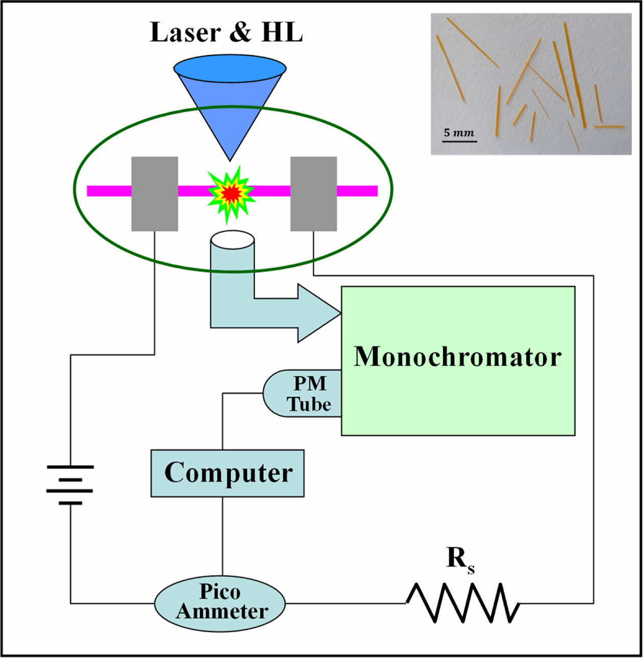
The crystal structure of the grown crystals was fulfilled through x-ray diffraction (XRD). In order to take out information about molecular vibrations and the crystal structure, the PC/PL spectra induced by an electric field were measured. Two indium electrodes with coplanar geometry were fabricated on the CdS specimens using an e-beam evaporator, and ohmic contact of the electrodes was confirmed by current–voltage measurements. The distance between the electrodes was 1 mm. Fig. 1 presents the schematic diagram of the PC/PL measurement device. At this time, the measurement of PC/PL was varied from 0 to 200 V/cm. Thus, PC/PL experiments were carried out at room temperature while scanning the wavelength from 300 to 900 nm. PC measurement was carried out under illumination by monochromatic light from a halogen lamp (HL, output power 500 W). The monochromatic light was normalized, and its intensity was 18l W/cm2. The excitation wavelength for PL measurements was 442 nm that was emitted from a He–Cd laser (Kimmon, 100 mW). The laser beam was illuminated on the surface between the electrodes of the PC specimen. While carrying out the PL experiment, the PC measurement was simultaneously completed. In addition, the subfigure picture in Fig. 1 shows that the dimensions of each needle-shaped rod are 4 to 17 mm long with a diameter of less than 100 mm.
|
Fig. 1 Schematic diagram of the PL/PC measurement device. The subfigure shows the photograph of the needle-shaped CdS rod. (Here, HL is a halogen lamp). |
PC characteristic
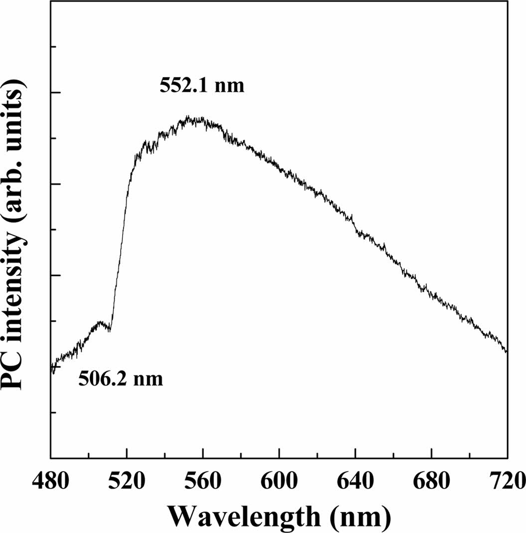
Fig. 2 shows the PC spectrum obtained at an applied electric field of 30 V/cm. As shown in Fig. 2, two peaks at short and long wavelength region were observed. In PC measurements, when the incident photon energy is greater than the bandgap energy, the absorbed photons produce electron and hole carriers in the CdS specimen. When an external electric field is applied, electrons move rapidly towards the anode and holes move towards the cathode owing to the electric field caused by the bias voltage. Then, these carriers produce a spectral PC peak. As the wavelength increases, there is a transition from surface excitation to volume excitation. This transition created the largest peak in the PC spectrum. This PC peak corresponds to one of several mechanisms: band-to-band transitions, impurity levels to band edge transitions, ionization of donors, and deep levels in the bandgap [20]. Furthermore, excitons are caused by the attraction between a hole and an electron when the carrier concentration is low [21], however, electrons that contribute to excitons trend to disappear easily due to the mutual interaction between them, when the carrier concentration is high. At our work, the CdS specimen is a low-order electron carrier of 1016 cm-3. Based on these facts, it suggests that one peak of low intensity at 2.4493 eV (506.2 nm) of the short wavelength region corresponds to the exciton spectrum caused by band-to-band transition. This exciton peak is a close to the value of 2.4455 eV obtained by PL measurement [22].
The other hand, the other peak of 2.2457 eV (552.1 nm) at the long wavelength region, which exhibits a broad and strong intensity, is thought to originate from the native defects in the crystal. These native defects are originated by imperfection defects, including vacancies, interstitial atoms, and dislocations, etc. Imperfection defects were formed due to structural deviations from the atomic arrangement of the perfect crystal.
PL characteristic
Fig. 3 presents the PL spectra of the needle-shaped CdS rod measured under several electric fields. This measurement was carried out under electric fields ranging from 0 to 200 V/cm. As shown in Fig. 3, the PL spectrum of the 0 V/cm label measured in the absence of an electric field at room temperature has two broadened peaks, and a low intensity peak and a high intensity peak were observed at a short and long wavelengths, respectively. From the upper PC result, it suggests that a low intense peak at 2.4489 eV (506.3 nm) in the short wavelength region corresponds to the exciton emission. Generally, exciton is thermally disso- ciated when the thermal energy exceeded the binding energy of exciton. Therefore, when temperature is high, the linewidth of exciton peak tends to be broadened due to the increase of the impurity scattering in the crystal. Consequently it is difficult to observe the exciton peak at the room temperature. It means that the needle-shaped CdS rod was grown to the high quality crystal. The broad peak in 530-590 nm (it is called the green band) regions observed in the long wavelength region is then considered to be due to defect-related peak occurring in the S-vacancy (or Cd-interstitial) atom. Therefore, a donor level of 0.21 eV below the conduc- tion band is thought to be related to these defect atoms [23]. As can be shown in Fig. 3, the peak positions of the exciton spectrum measured at different electric fields tended to shift to the long wavelength region as the electric field increased, and theirs intensity decreased. At the spectrum of 200 V/cm, the exciton peak was posited to 2.4392 eV (508.3 nm). During an electric field change from 0 to 200 V/cm, the exciton emission has a peak shift of about 8.7 meV.
Combined EFI PC/PL analysis
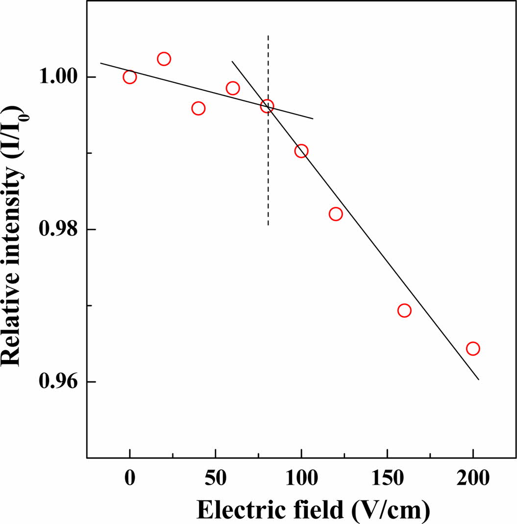
Fig. 4 plots the relative intensities of the exciton emission compared with varying electric field. Here, I and Io mean the intensity of the exciton emission with and without the applied electric field, respectively. As shown in Fig. 4, the relative intensity of the exciton emission tended to decrease with increasing electric field. Thus, relative intensities are steeply quenching at the electric field over 80 V/cm while these show the gentle slope below electric fields of 80 V/cm. This indicates that there exists a strong correlation at the electric field over 80 V/cm.
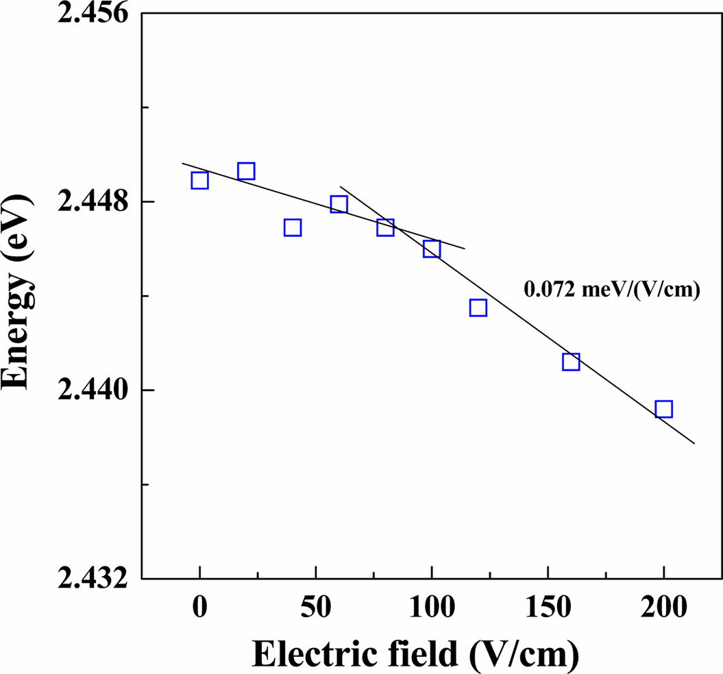
Fig. 5 displays the peak energy of the exciton emission obtained with varying electric field. As shown in Fig. 5, exciton peak energies tend to shift toward the lower energy region (red shift) with increasing electric field, and its shift energy is about 8.7 meV. In particular, this energy varies slightly in the electric field up to 80 V/cm, but in electric fields above 80 V/cm, it moves rapidly towards the lower energy region.
Since the above behaviors are related to the PC effect, the intensity decrease and peak shift for exciton emissions can be well understood by explaining the PC mechanism. In this experiment, it was thought that PL and PC measurements were performed simultaneously. PC measurements were performed with a unique light of 442 nm during PL measurements in various electric fields. When photons with energies greater than the bandgap energy of a semiconductor are incident upon a photoconductive material, electrons and holes are created in the conduction and the valence bands, respectively [20]. The carriers of the created electrons and holes are immediately guided to the electrodes on both sides. PC carriers appear as currents generated by these photocreated electrons and holes. Thereby, the decrease in intensity and the shift of the peak to low energy region are closely related to the mechanism that generates electrons and holes. As mentioned above, the intensity reduction and peak shift of the exciton emission decreases rapidly in electric fields above 80 V/cm, while they decrease gently in electric fields below 80 V/cm. Here, the electric field of 80 V/cm can be called a turning point that is strongly dependent on the applied electric field. PC carriers of free electrons and holes, created by absorption of light with energy greater than the bandgap energy, affect the conduction band and the valence band, respectively. These PC carriers accelerate gradually as the external electric field increases. Thus, the generated and accelerated PC carrier readily interacts with the free excitons transited by the excitation source of PL, so this situation prevents direct recombination and shortens the lifetime of the free excitons. Consequently, a decrease in PL intensity is associated with a decrease in recombination of free exciton. This fact was also observed by Jeong et al. [24]. They explained that the damping of Raman modes is caused by the phonon-hole scattering due to a strong interaction between the phonons and the photogenerated hole carriers with increasing the applied electric field.
Exciton emission influenced by the electric field
The exciton peak energy in Fig. 5 tends to move to the lower energy region as the electric field increases. It is believed that the PC carriers screen the PL emissions while the electric field increases. Thereby, the PL emissions involve a spatially indirect recombination. Naturally the number of carriers participating in recom- bination will be reduced. Such recombination should yield a linear red Stark shift, which relates to a change in the atomic energy on application of an electric field [25]. Here, the Stark effect arises due to the interaction between the electric moment of the atom and the external electric field [26]. The amount of splitting and or shifting is called the Stark splitting or Stark shift. Furthermore, the stark effect describes that two energy states that have the same energy can be split up using an electric field. Therefore, an electric field can help to distinguish degenerate eigenstates in a physical system. In general, it is divided into the first-order Stark effect and the second-order Stark effect. The first order effect is linear in the applied electric field. It is the series of spectral lines that are produced when transitions between the energy levels are symmetric. A second order effect occurs when a dipole moment is induced by an external electric field, but is quadratic in the field. A quadratic stark effect is a series of spectral lines with asymmetric line patterns. So, the energy level difference (∆e) appears to be proportional to the square of the applied electric field, that is ∆ε∝Ε2. The effect of an external electric field on the PL spectrum was investigated by several research groups [27-30]. It was found that the PL intensity is quenched by the external electric field. The reduction in the PL intensity is expected as the electric-field induced tilting of the quantum well energy bands results in the reduction in the overlap of the electron and hole wave functions. Fafard et al. [30] have shown that the external field-induced quenching and peak shift may be altered by varying the excitation intensity. They have attributed these effects to a local flattening of the bands in the well region induced by the screening of the carriers trapped in the well. As shown in Fig. 5, the peak shift of the exciton emission decreases rapidly in electric fields above 80 V/cm and theirs peak energy decreases linearly with a slope of 0.072 meV/(V/cm) in an electric field above 80 V/cm. This phenomenon indicates that the first order Stark effect was observed in our work. Consequently, this strong interaction between free excitons and photogenerated PC carriers due to electric field has been interpreted as leading to a shift or broadening of the spectrum. Moreover, these interactions naturally cause a loss of intensity and red shift in the exciton spectrum. These results concluded that the intensity quenching and red shift of the exciton peak were strongly related to the electric field. However, no emission shift due to the electric field was founded for the defect-related peaks at long wavelength region.
|
Fig. 2 PC spectrum measured at 30 V/cm electric fields. |

|
Fig. 3 PL spectra of the needle-shaped CdS rod measured under several electric fields. |
|
Fig. 4 Relative intensity of the exciton emission compared with varying electric field. Here, I and Io mean the intensity of the exciton emission with and without the applied electric field, respectively. Also, the PC is measured under illumination with a unique light of 442 nm. |
|
Fig. 5 Exciton energy of the exciton emission obtained with varying electric field. |
The behaviors of the exciton-electron scattering on the needle-shaped CdS rod grown using the vapor phase technique were analyzed through the EFI PC/PL experiments. The intensity of the exciton spectrum decreased as the external electric field increased, and also rapidly dissipated in the electric field above 80V/cm. Thus, exciton peak energy had a red shift as the electric field increases. Its shift gap was about 8.7 meV. The behavior of the exciton emissions was found to depend strongly on the electric field applied. The combined results of PC/PL measurements suggest that the excitons readily interact with the PC carriers of the photocreated electrons and holes. This interaction disturbs the direct recombination of the excitons. Consequently, the PL intensity quenching is related to a decrease in the recombination of the exciton. Thus, these PL emissions involve a spatially indirect recombination. The number of carriers participating in recombination should be naturally reduced. Such recombination should yield a linear red Stark shift, which relates to a change in the atomic energy on application of an electric field. We found that this phenomenon occurs in exciton–electron scattering caused by a strong interaction between excitons and photogenerated electron carriers with increasing the applied electric field.
- 1. H. Liu, J. Lu, Z. Yang, J. Teng, L. Ke, X. Zhang, L. Tong, and C. H. Sow, Sci. Rep. 6 (2016) 27387.
-

- 2. M. Moghaddam, N. Nadere, M. Hosseinifard, and A. Kazemzadeh, Ceram. Int. 46 (2020) 7388-7395.
-
- 3. Y.-J. Choi, I.-S. Hwang, J.-H. Park, S. Nahm, and J.-G. Park, Nanotechnology 17 (2006) 3775-3778.
-
- 4. A. Pan, H. Yang, R. Liu, R. Yu, B. Zou, and Z. Wang, J. Am. Chem. Soc. 127 (2005) 15692-15693.
-
- 5. J.A. Zapien, Y.K. Liu, Y.Y. Shan, H. Tang, C.S. Lee, and S.T. Lee, Appl. Phys. Lett. 90 (2007) 213114.
-
- 6. A. Pan, W. Zhou, E.S.P. Leong, R. Liu, A.H. Chin, B. Zou, and C.Z. Ning, Nano Lett. 9 (2009) 784-788.
-
- 7. Y. Lu, F. Gu, C. Meng, H. Yu, Y. Ma, W. Fang, and L. Tong, Opt. Express 21 (2013) 22314-22319.
-
- 8. X. Zhuang, C.Z. Ning, and A. Pan, Adv. Mater. 24 (2012) 13-33.
-
- 9. G. Vincent, A. Chantre, and D. Bois, J. Appl. Phys. 50 (1979) 5484.
-
- 10. R.E. Hetrick and K.F. Yeung, J. Appl. Phys. 42 (1971) 2882.
-
- 11. S.-J. Park, S. Lingk, W.L. Miller, A. Gesquiere, and P.F. Barbara, Chem. Phys. 341 (2007) 169-174.
-
- 12. R.G. Ulbrich, Solid State Electron. 21 (1978) 51-59.
-
- 13. D. Li, J. Zhang, Q. Zhang, and Q. Xiong, Nano Lett. 12 (2012) 2993-2999.
-
- 14. K. Sarmah, R. Sarma, and H.L. Das, J. Non Oxide Glasses 1 (2009) 131-141.
- 15. J. Chen, J.J. Lu, R. Zhang, Y.S. Liu, and W.Z. Shen, Phys. Stat. Sol. (b)248 (2011) 1718-1722.
-
- 16. Y. Kuo, J. Li, X. Michalet, A. Chizhik, N. Meir, O. Bar-Elli, E. Chan, D. Oron, J. Enderlein, and S. Weiss, ACS Photonics 5 (2018) 4788-4800.
-
- 17. M.S. Mehata, Sci. Rep. 5 (2015) 12056.
-
- 18. Y. Lee, S. Kim, H.S. Kim, J.B. Shin, W. Choi, H. Cho, K. Kim, T. Lee, J. Kim, I-B. Kang, K.C. Choi, Y-H. Kim, and D.Y. Jeong, J. Mater. Chem. C5 (2017) 2098-2106.
-
- 19. Z. Liu, C.-H. Lin, B.-R. Hyun, C.-W. Sher, Z. Lv, B. Luo, F. Jiang, T. Wu, C.-H. Ho, H.-C. Kuo, and J.-H. He, Light. Sci. Appl. 9 (2020) 83.
-
- 20. N.V. Joshi, in “Photoconductivity: Art, Science, and Technology” (Marcel Dekker, 1990) p.4.
-
- 21. R.A. Smith, in “Semiconductors, 2nd Ed.” (Cambridge University Press, 1978) p.72.
- 22. T.S. Jeong, P.Y. Yu, and T.S. Kim, J. Korean Phys. Soc. 36 (2000) 102-105.
- 23. T. Sivaraman, V.S. Nagarethinam, and A.R. Balu, Res. J. Material Sci. 2 (2014) 6-15.
- 24. T.S. Jeong, C.J. Youn, M.S. Han, J.W. Yang, and K.Y. Lim, Appl. Phys. Lett. 83 (2003) 3483.
-
- 25. J.I. Pankove, in “Optical processes in semiconductors” (Dover, 1975) p.28.
- 26. https://www.differencebetween.com/what-is-the-difference-between-linear-and-quadratic-stark-effect/ (accessed May 31, 2021)
- 27. R.C. Miller and A.C. Gossard, Appl. Phys. Lett. 43 (1983) 954.
-
- 28. L. Via, R.T. Collins, E.E. Mendez, and W.I. Wang, Phys. Rev. B 33 (1986) 5939.
-
- 29. R.B. Santiago, J. d’Alburquerque e Castro, and L.E. Oliviera, Phys. Rev. B 48 (1993) 4498.
-
- 30. S. Fafard, E. Fortin, and J.L. Merz, Phys. Rev. B 48 (1993) 11062.
-
 This Article
-
2022; 23(2): 132-136
Published on Apr 30, 2022
- 10.36410/jcpr.2022.23.2.132
- Received on Apr 29, 2021
- Revised on Sep 24, 2021
- Accepted on Sep 25, 2021
Services
Shared
Correspondence to
- T.S. Jeong
-
Semiconductor Physics Research Center (SPRC), School of Semiconductor and Chemical Engineering, Jeonbuk National University, Jeonju 54896, Korea
Tel : +82 63 270 3326 Fax: +82 63 270 3585 - E-mail: tsj@chonbuk.ac.kr
Clean-Energy Research Institute(CRI), Hanyang University, 222, Wangsimni-ro, Seongdong-gu, Seoul, 04763, Korea
E-mail: jcpr@hanyang.ac.kr