


- Dielectric properties of KTN(80/20) thin films with pzt buffer layer for tunable microwave devices
Kyeong-Min Kima,#, Sam-Haeng Leea,b,#, Byeong-Jun Parka, Joo-Seok Parkb and Sung-Gap Leea,*
aDept. of Materials Engineering and Convergence Technology, RIGET, Gyeongsang National University, Jinju 52828, Korea
bBusiness Cooperation Center, Korea Institute of Ceramic Engineering and Technology, Jinju 52851, KoreaThis article is an open access article distributed under the terms of the Creative Commons Attribution Non-Commercial License (http://creativecommons.org/licenses/by-nc/4.0) which permits unrestricted non-commercial use, distribution, and reproduction in any medium, provided the original work is properly cited.
K(Ta0.80Nb0.20)O3 films with Pb(Zr0.52Ti0.48)O3PZT buffer layer on Pt/Ti/SiO2/Si substrate were fabricated by sol-gel and spin-coating method. Structural and electrical properties were measured with variation of the sintering temperature, and the applicability to microwave materials was investigated. All K(Ta0.80Nb0.20)O3 films showed a cubic crystal structure. Average grain size was about 123~193 nm and average thickness of the K(Ta0.80Nb0.20)O3 films was approximately 366 nm. Through the AFM results, root mean square roughness (Rrms) of all K(Ta0.80Nb0.20)O3 films was around 6 nm. All K(Ta0.80Nb0.20)O3 films showed a tendency to increase dielectric loss as frequency increased. As the sintering temperature increased, tunability with an applied DC voltage indicated a decreasing tendency. Tunability and temperature coefficient of the K(Ta0.80Nb0.20)O3 film sintered at 700 oC showed good values of 22.1% at 10 V, -0.594/oC
Keywords: K(Ta0.80Nb0.20)O3, Microwave tunable devices, Buffer layer, Sol-gel, Spin coating
Ferroelectric thin films exhibiting nonlinear dielectric properties with variation of an applied electric field can be applied to various tunable microwave devices. In particular, since KTa1-xNbxO3 (KTN) material having a perovskite crystal structure exhibits various ferroelectric properties depending on the composition ratio, many studies are being conducted for application to band filter, IR sensors, and electro-optic devices [1, 2]. And many researchers are conducting investigations for the application of KTN materials to microwave devices by using the high dielectric constant, low dielectric loss, and the variation of the phase transition temperature (Tc) according to the Ta/Nb composition ratio [3-6]. Structural and electrical properties of KTN thin films have a highly dependency on the crystal structure and lattice parameter of the substrates, and many studies have been conducted using (100) MgO and (100)/(110) SrTiO3 single crystals [7, 8]. In addition, KTN films were fabricated on Si-based substrates using various buffer layers such as KNbO3, PZT, Al2O3 [9-12].
Dielectric materials require high and stable dielectric constant at microwave frequencies, low dielectric loss, and high tenability (change in dielectric constant with applied field) properties for application to microwave tunable devices [13]. In addition, structural properties such as surface uniformity and densification have a great influence on the electrical properties of microwave devices [14]. In this study, we fabricated KTa0.80Nb0.20O3 films using a chemical solution deposition (CSD) method, which has the advantages of a relatively simple equip- ment, large area possible, and easy composition control. And, PbZr0.52Ti0.48O3 film was used as a buffer layer to improve the crystallization of KTN film on Pt/Ti/SiO2/Si substrate. Structural and electrical properties of KTN films were studies for application to microwave tunable devices.
KTa0.80Nb0.20O3 precursor solutions were synthesized from potassium acetate, niobium ethoxide, tantalum ethoxide with 2-methoxyethanol used as a solvent. The molar concentration of solution was adjusted to 0.3 M, and 10 mol% of excess potassium acetate was added to compensate for the K2O losses during annealing. PbZr0.52Ti0.48O3 coating solution was prepared by the same synthesis process as in the previous research [15]. KTN films were fabricated on the PZT-buffered Pt/Ti/SiO2/Si substrates through a repeated spin coated at 3,500 rpm for 30 sec, followed by a drying at 200 oC for 5 min, pyrolysis at 400 oC for 15 min, and followed with rapid thermal annealing (RTA) between 700~850 oC for 30 min in an oxygen atmosphere. The surface and cross-sectional microstructures of KTN films were observed using field-emission scanning electron micro- scope (FE-SEM) and atomic force microscopy (AFM). The crystallographic properties were determined using an X-ray diffractometer (XRD). Pt upper-electrode with a diameter of 500 μm was deposited on KTN films using dc sputtering method, and then electrical properties were measured using an LCR meter.
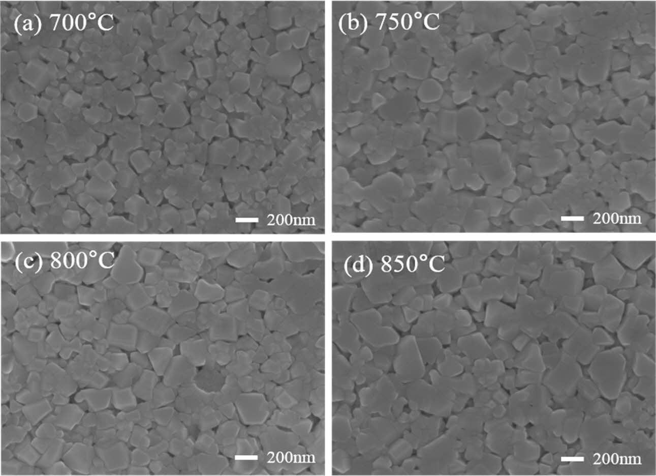
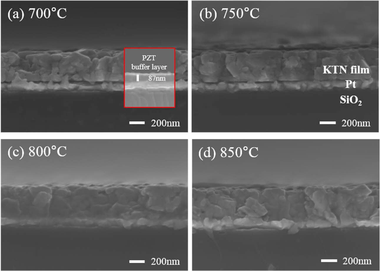
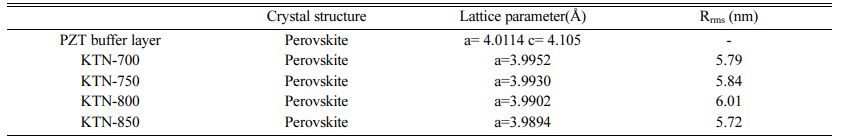
Fig. 1 shows the XRD patterns of KTN films deposited on the PZT-buffered Pt/Ti/SiO2/Si, annealed at various temperatures in the range of 700~850 oC. All KTN films showed only the (100) and (200) diffraction peaks, which indicates the formation of films with preferentialorientation to the (100) plane. Also, as the annealing temperature increases, the peak intensity of KTN films was gradually increased and the lattice parameter calculated from the distance of (100) planes was decreased from 3.9952 to 3.9894 Å (Table 1). It is well known that crystallization and orientation of KTN films with the desired crystalline structure were strongly dependent on the crystal structure of the lower layer [7]. Using the PZT-buffer layer with similar crystal structure and lattice parameter, highly (100)-oriented KTN films were obtained. SEM surface images of KTN films annealed at various temperatures are shown in Fig. 2. All specimens showed surface morphologies with relatively uniform sized grains, and exhibited a dense microstructure without pores inside the specimen as shown in the cross-sectional morphologies. And the average grain size [17] increases from 123 nm to 193 nm as the sintering temperature increases. Fig. 3 exhibits the cross-sectional SEM image of KTN films with PZT buffer layer grown on Pt/Ti/SiO2/Si. Thickness of all KTN films are around 366 nm. As sintering temperature increases, the interface layer among Pt, PZT buffer layers and KTN films seem to be become blurred.
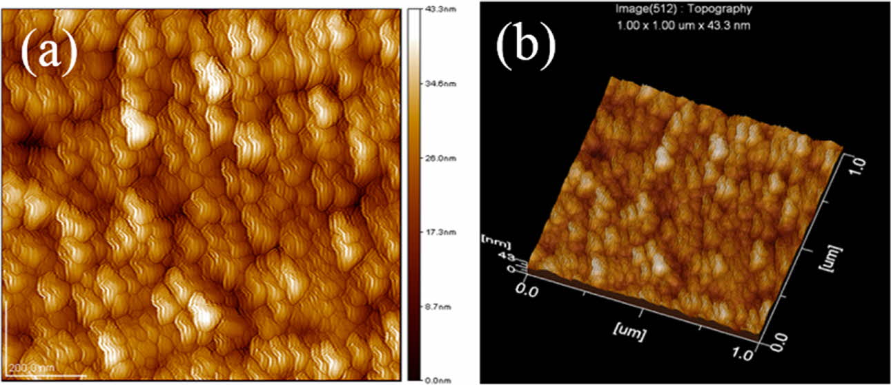
Fig. 4 shows (a) 2D and (b) 3D AFM images of the KTN film annealed at 800°C. All KTN films exhibited a dense microstructure without cracks or defects and root mean square roughness (Rrms) showed good property of about 6 nm. Generally, the surface flatness and uniformity of the specimen are very important parameters because the leakage current and electrical resistivity of microwave tunable devices greatly depend on the structural properties of the surface and/or interface [16, 18].
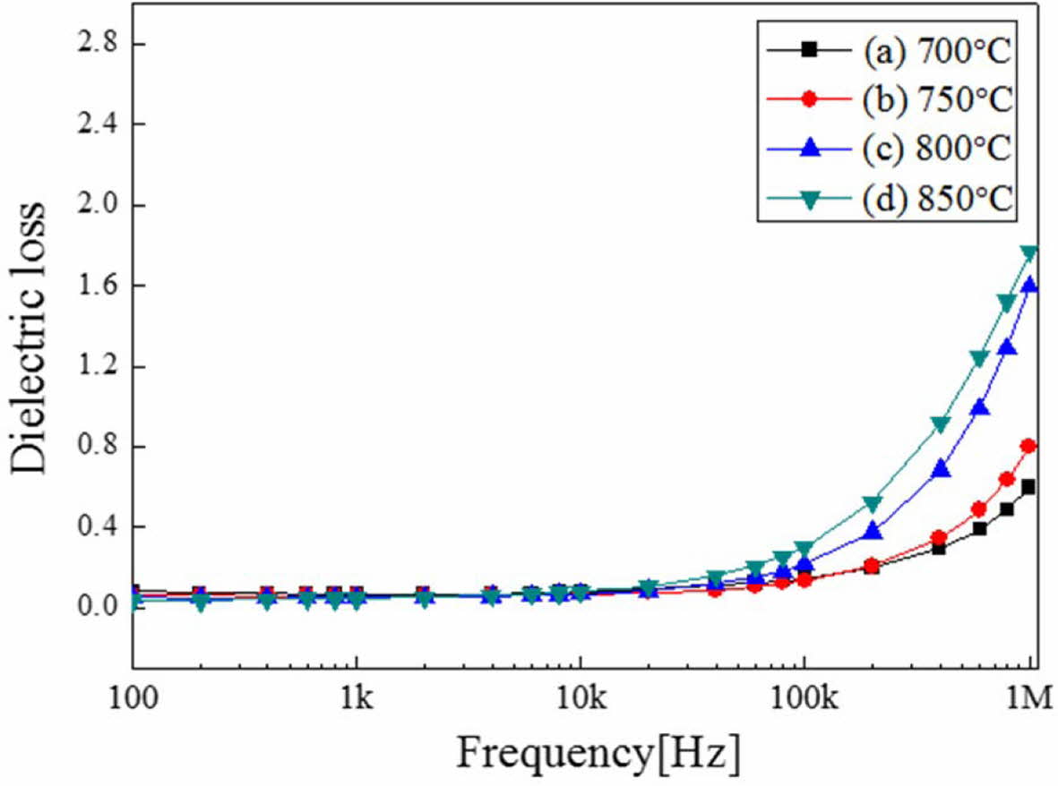
Fig. 5 shows the dielectric loss of the KTN films with the variation of frequency. In the vicinity of the low frequency, the relatively low dielectric loss is shown in all KTN films, but the higher the frequency, the dielectric losses of the KTN films sintered at 800, 850 oC tends to decrease significantly. It can be inter- preted in two cases. As the sintering temperature of the KTN films increases, first, the increase in dead layer thickness due to ion diffusion of PZT/Pt interfaces affects extra loss [19, 20]. Second, the loss mechanism that significantly contributes to loss in tunable micro- wave materials can be described as charge defect. The oxygen vacancies are increased by the volatilization of Pb, K ions, which increases dielectric loss [21, 22].
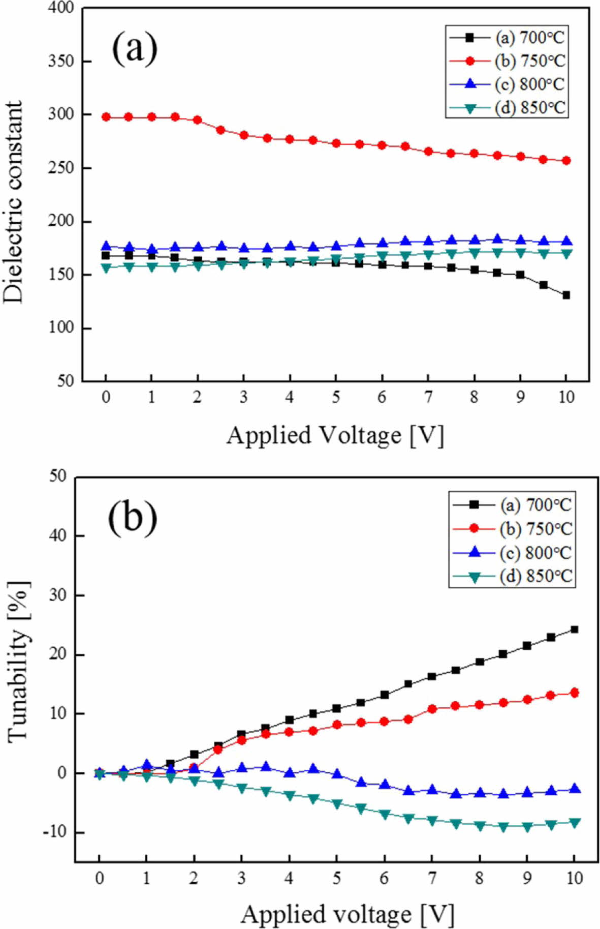
Fig. 6 shows (a) dielectric constant and (b) tunability of the KTN films by applied DC voltage. The dielectric constant conventionally decreases as the applied voltage increases due to a clamping effect suppressing the rotation and displacement of dipoles by an externally applied DC electric field. The % tunability was deter- mined using the following equation [23]; % tunability = {ε(0)-ε(E0)}/ε(0), where ε(0) is the dielectric constant without a DC bias and ε(E0) is the dielectric constant with E0 bias. As shown in Fig. 6(a), dielectric constant increased with increasing the sintering temperature due to the growth of high permittivity grain and increase of the homogeneity of structure. However, dielectric constant decreased above 800 oC, and it is considered to be due to the inhomogeneity of composition and structure by diffusion of K and Pb ions with low melting point in the KTN/PZT interfaces. Tunability decreased with increasing sintering temperature, especially the specimen sintered over 800 oC show negative values, as shown in Fig. 6(b). This is considered to be due to the increase in ionic displacement according to the applied electric field for the formation of an interface layer with a low permittivity due to diffusion of K and Pb ions, and the inhomogeneity of composition and structure.
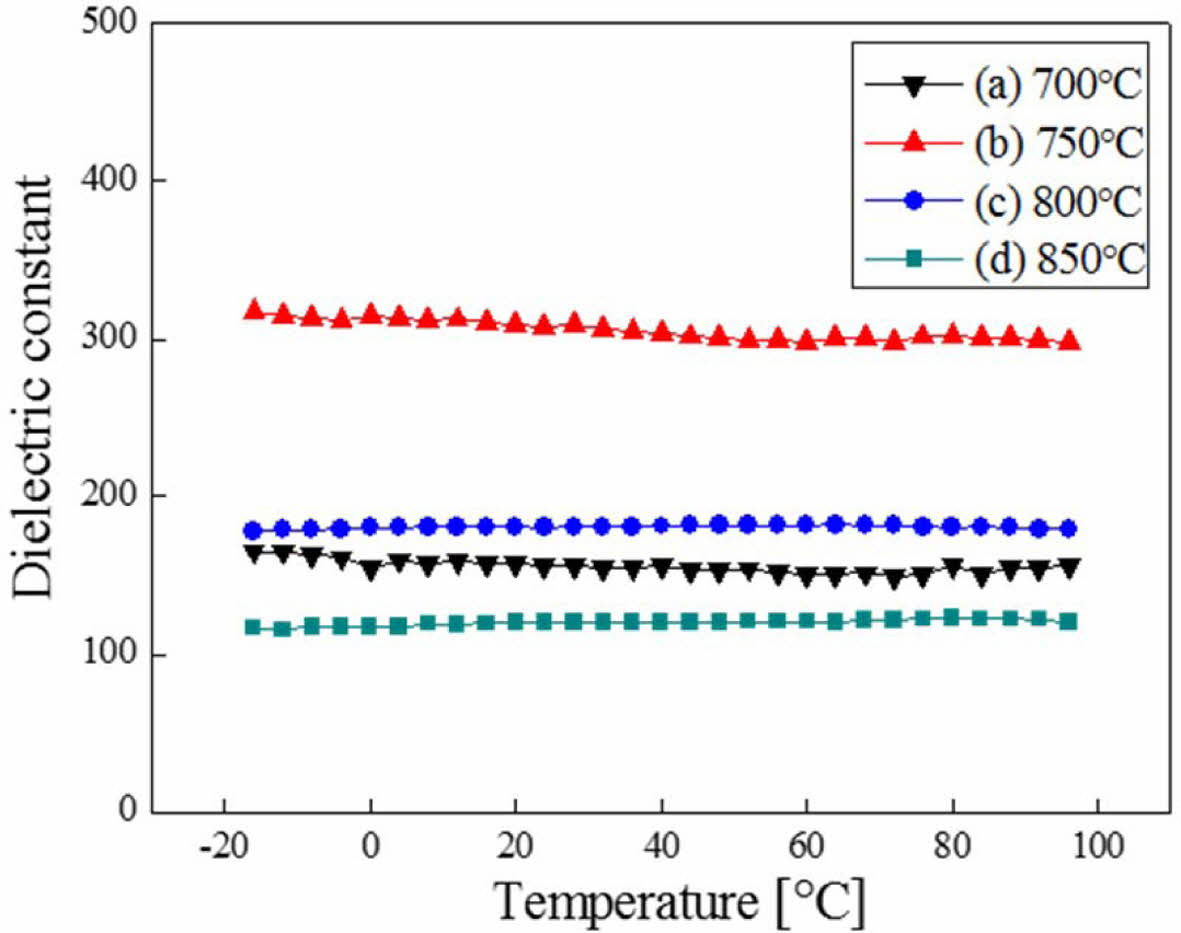
Fig. 7 shows the temperature dependence of the dielectric constant of KTN films, measured between -16 and 96 oC. In general, the temperature-dielectric constant properties of ferroelectric materials show a strong temperature dependence around the phase transi- tion temperature according to the Curie-Weiss law. However, KTN/PZT multilayer films showed very good properties with low temperature dependence in the measurement temperature range. This is thought to be because the paraelectric KTN film suppressed the tem- perature-dependent change properties of the ferroelec- tric PZT film [14]. The KTN film sintered at 700 oC showed an excellent temperature coefficient of -0.594/oC.

|
Fig. 1 XRD of K(Ta0.8Nb0.2)O3 thin films with the variations of sintering temperature. |
|
Fig. 2 Surface images of K(Ta0.8Nb0.2)O3 thin films with the variations of sintering temperature. |
|
Fig. 3 Cross-sectional images of K(Ta0.8Nb0.2)O3 thin films with the variations of sintering temperature. |
|
Fig. 4 Atomic Force Microscopy 2D (a) and 3D (b) surface topographies of KTN films grown at 800°C on PZT-buffered Pt/ Ti/SiO2/Si substrates. |
|
Fig. 5 Frequency dependence of dielectric loss of K(Ta0.8Nb0.2)O3 thin films with variations of sintering temperature. |
|
Fig. 6 Applied voltage dependence of (a) dielectric constant and (b) tunability of K(Ta0.8Nb0.2)O3 thin films with the variations of sintering temperature. |
|
Fig. 7 Temperature dependence of dielectric constant of K(Ta0.8Nb0.2)O3 thin films with variations of sintering temperature |
|
Table 1 Structural properties of KTN thin films with the variation of the annealing temperature |
The KTN films were grown on Pt/Ti/SiO2/Si substrate by chemical solution deposition with a PZT buffer layer. All KTN films, fabricated with the variation of sintering temperature, had an (100) oriented polycrystalline cubic structure with relatively homogeneous surface. As sintering temperature increased, the crystallinity of the KTN film increased, but due to ion diffusion between electrode and PZT it showed that the increase in the dead layer degrades electrical properties. The dielectric loss, tunability and temperature coefficient of the KTN film sintered at 700 oC showed optimum values of 0.798, 22.1% at 10 V and -0.594/oC.
This research was supported by Basic Science Re- search Program through the National Research Foundation of Korea (NRF) funded by the Ministry of Education (2020R1A6A1A03038697) and This work was supported by the National Research Foundation of Korea (NRF) grant funded by the Korea government (MSIT) (2021 R1I1A3052426).
- 1. S. Yagi, K. Fujiura, Electro-optic KTN devices, Physics Procedia 56 (2014) 40-47.
-

- 2. B. Park, S. Lee, J. Kim, J. Park, S. Lee, J. Ceram. Proc. Res. 22[2] (2021) 214-220.
-
- 3. T. Imai, M. Sasaura, K. Nakamura, and K. Fujiura, NTT Technical Review 5[9] (2007) 1-8.
- 4. S. Glinšek, I. Arčon, B. Malič, A. Kodre, M. Kosec, J. Solgel Sci. Technol. 62[1] (2012) 1-6.
-
- 5. J. Fisher, K. Lee, W. Moon, J. Ceram. Proc. Res. 21[1] (2020) 5-13.
-
- 6. V. Laur, G. Tanné, P. Laurent, A. Rousseau, V. Bouquet, M. Guilloux-Viry, F. Huret, Ferroelectrics 353[1] (2007) 21–28.
-
- 7. A. Nazeri, M. Kahn, J. Am. Ceram. Soc. 75[8] (1992) 2125-2133.
-
- 8. J. Buršík, I. Drbohlav, P. Vaněk, V. Železný, J. Eur. Ceram. Soc. 24[2] (2004) 455-462.
-
- 9. W. Peng, M. Guilloux-Viry, S. Députier, V.Bouquet, Q. Simon, A. Perrin, A. Dauscher, S. Weber, Appl. Surf. Sci. 254[4] (2007) 1298-1302.
-
- 10. W. Peng, V. Bouquet, S. Deputier, Q. Simon, M. Guilloux-Viry, A. Perrin, Integr. Ferroelectr. 93[1] (2007) 126-132.
-
- 11. M. Kwon, S. Lee, K. Kim, S. Choi, J. Ceram. Proc. Res. 20[6] (2019) 603-608.
-
- 12. T. Ohno, M. Fujimoto, T. Ota, M. Fuji, M. Takahashi, H. Suzuki, J. Eur. Ceram. Soc. 26[10-11] (2006) 2143-2146.
-
- 13. A. Ahmed, I.A. Goldthorpe, and A.K. Khandani Appl. Phys. Rev. 2[1] (2015) 011302.
-
- 14. S. Gevorgian, P.K. Petrov, Z. Ivanov, and E. Wikborg, Appl. Phys. Lett. 79 (2001) 1861.
-
- 15. S.H. Jo and S.G. Lee, J. Ceram. Process. Res. 13 (2012) 631-634.
- 16. Y.S. Kim, M.Y. Sung, Y.H. Lee, B.K. Ju, and M.H. Oh, J. Electrochem. Soc. 146[9] (1999) 3398-3402.
-
- 17. G. Vander Voort, Microsc. Microanalysis 19 (2013) 1760-1761
-
- 18. A.S. Daryapurkar, J.T. Kolte, P. Gopalan, Ferroelectrics 447 (2013) 46–55.
-
- 19. Y.W. Cho, S.K. Choi and G. Venkata Rao, Appl. Phys. Lett. 86 (2005) 202905
-
- 20. W. Hu, C. Yang, W. Zhang, G. Liu, D. Dong, J. Solgel Sci. Technol. 39[3] (2006) 293-298.
-
- 21. M.W. Cole, P.C. Joshi, and M.H. Ervin, J. Appl. Phys. 89 (2001) 6336.
-
- 22. Z. Yuan, Y. Lin, J. Weaver, X. Chen and C.L. Chen, G. Subramanyam, J.C. Jiang, E.I. Meletis, Appl. Phys. Lett. 87 (2005) 152901.
-
- 23. Y. Chen, L. Wu, C. Huang, Y. Chou and Y. Tsai, Jpn. J. Appl. Phys. 39[5A] (2000) 2690-2695.
-
 This Article
-
2022; 23(1): 29-32
Published on Feb 28, 2022
- 10.36410/jcpr.2022.23.1.29
- Received on May 18, 2021
- Revised on Oct 5, 2021
- Accepted on Oct 9, 2021
Services
- Abstract
introduction
experimental
results and discussion
conclusions
- Acknowledgements
- References
- Full Text PDF
Shared
Correspondence to
- Sung-Gap Lee
-
Dept. of Materials Engineering and Convergence Technology, RIGET, Gyeongsang National University, Jinju 52828, Korea
Tel : +82-55-772-1687 Fax: +82-55-772-1689 - E-mail: lsgap@gnu.ac.kr
Clean-Energy Research Institute(CRI), Hanyang University, 222, Wangsimni-ro, Seongdong-gu, Seoul, 04763, Korea
E-mail: jcpr@hanyang.ac.kr