


- Effect of TiO2 photoelectrode thickness on the performance of dye-sensitized solar cells
Woon-Yong Parka and Ki-Tae Leea,b,c,*
aDivision of Advanced Materials Engineering, Jeonbuk National University, Jeonbuk 54896, Republic of Korea
bDepartment of Energy Storage/Conversion Engineering of Graduate School, Jeonbuk National University, Jeonbuk 54896, Republic of Korea
cHydrogen and Fuel Cell Research Center, Jeonbuk National University, Jeonbuk 54896, Republic of KoreaThis article is an open access article distributed under the terms of the Creative Commons Attribution Non-Commercial License (http://creativecommons.org/licenses/by-nc/4.0) which permits unrestricted non-commercial use, distribution, and reproduction in any medium, provided the original work is properly cited.
TiO2 photoelectrodes for dye-sensitized solar cells (DSSCs) were fabricated by changing the thickness using screen printing method. The amount of dye adsorbed on TiO2 increases as the thickness of the TiO2 photoelectrode increases because of the increase in the dye molecule adsorption site. The performance of DSSCs increases up to a TiO2 thickness of approximately 12 μm, indicating a tendency of dye adsorption that enables photocurrent generation. However, when TiO2 is thicker than 12 μm, the TiO2 films start to break, resulting in a decrease in the performance. The optimum thickness of the TiO2 photoelectrode was 12 μm, which has a low charge transfer resistance
Keywords: dye-sensitized solar cells, photoelectrode, TiO2, screen printing, dye adsorption
Dye-sensitized solar cells (DSSCs) are one of the most attractive solar cells because of their low manu- facturing cost, high conversion efficiency, and wide application compared with conventional silicon-based solar cells [1-4]. A conventional DSSC is composed of a photoelectrode, counter electrode, dye, and electrolyte [5]. The TiO2 photoelectrode specifically generates photocurrent by absorbing the light, which is one of the most important factors of DSSCs. The material of the photoelectrode is an n-type semiconductor oxide with a wide energy band gap of 3–4 eV, such as TiO2, ZnO, and SnO2 [6-10]. TiO2 is the most widely used ceramic material for photoelectrodes because of its large surface area in adsorbing dye molecules, suitable band edge levels for charge injection/extraction, and high chemical stability [11-16]. Various factors affect the open-circuit voltage (VOC), short-circuit current density (JSC), and fill factor (FF), which are parameters that determine the photoelectric conversion efficiency. In particular, the thickness of the TiO2 photoelectrode is related to the transfer of electrons, diffusion, and generation of current, which are key factor that influence the overall perfor- mance of DSSCs [17-21, 22]. Therefore, the ceramic processing control to fabricate photoelectrode thin films is one of major issues to improve the performance of DSSCs.
In this study, TiO2 photoelectrodes with various thicknesses were fabricated by a screen printing method. Commercial TiO2 paste was also used because the efficiency and characteristics of the photoelectrode can be changed depending on the type of TiO2 paste. The electrical properties and efficiency of the cells were measured, and the electrochemical process inside the DSSC was analyzed. Finally, the change in DSSC mechanism with the thickness of TiO2 was confirmed using electrochemical analysis.
Fabrication of TiO2 photoelectrode
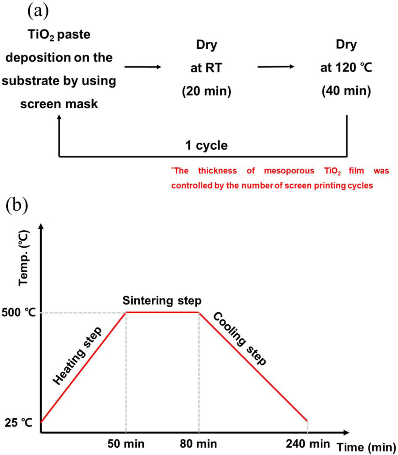
Fluorine-doped tin oxide (FTO)-coated glass (TEC 8, Pilkington, UK) with a sheet resistance of 6–9 Ω/□ was sequentially cleaned in acetone (99.5%, Daejung Chemicals and Metals Co., Korea), 2-propanol (99+%, Alfa Aesar, USA) and deionized (DI) water for 10 min each and dried using an air gun. A screen printing method was used with TiO2 paste (Ti-Nanoixde T/SP, Solaronix, Swiss) for mesoporous TiO2 film deposition. First, TiO2 paste was deposited using a screen printer. The screen-printed samples were dried at room temperature for 20 min and then dried again at 120 oC for 40 min in a dry oven to remove the organic solvent. As shown in Fig. 1(a), a series of steps constitutes one cycle, and the thickness is adjusted as the cycle repeats (1-6 cycles). After finishing the TiO2 paste deposition, the films were sintered at 500 oC for 30 min in an ambient atmosphere box furnace and the heating rate was 10 oC/min (Fig. 1(b)). The final thickness of the TiO2 film was controlled according to the number of screen printing cycles.
Assembly of DSSCs
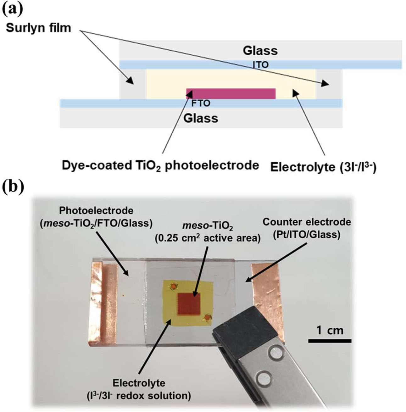
After finishing the sintering step, the TiO2 films were dipped with the prepared 0.3 mM (bis(tetrabutylammonium)-cis-di(thiocyanato)-N,N’–bis(4-carboxylato-4’-carboxylic acid-2,2-bipyridine) ruthenium (II) ethanol-based solution (N719, Solaronix, Swiss) in a dark field at room tempera- ture for 24 h. Before fabricating the counter electrode, two holes to inject the electrolyte were created in an indium-doped tin oxide (ITO)-coated glass (STN 10, UID, Korea) with a sheet resistance of 6-9 Ω/□, and then washed in the same process as for FTO/glass. Pt film as a counter electrode was deposited on the prepared ITO/glass using DC sputtering equipment (E-1030, Hitachi, Japan) at 25 mA and 30 s (the thickness of Pt: ~5 nm). For assembling the DSSC cells, the prepared photoelectrode and counter electrode were sealed using a 60 μm surlyn film (Solaronix, Switzerland). Electrolyte with the iodide/triiodide (I−/I3−) redox couple in acetonitrile solvent (AN-50, Solaronix) was injected through the holes. After finishing the electrolyte injection, the holes were enclosed by a cover glass or polyimide tape. The active area of TiO2 photoelectrode and electrolyte injection was 0.25 cm2 and 1.2 cm2, respectively. The final DSSC cells were denoted as TSP×1, TSP×2, TSP×3, TSP×4, TSP×5, and TSP×6 according to the number of screen printing cycles. The schematic diagram of the structure and a photograph of the DSSC cells are shown in Fig. 2.
Characterization
The thickness of the TiO2 films were analyzed by a high-resolution scanning electron microscope (HR-SEM, SU8230, Hitachi, Japan). Current-voltage (I–V) characteristics of the DSSCs were obtained under a standard illumination condition (100 mW/cm2 AM 1.5G) using source meter (Keithely 2400, Tektronix, Inc. USA) in the range of ±1 V, at a scan step of 0.02 V and during a delay time of 0.50 s. Electrochemical impedance spectroscopy (EIS) analysis was evaluated with a frequency range of 9 mHz to 100 kHz in a similar standard illumination condition using a potentiostat (SP150, Biologic SAS, France) to confirm the change in the electrochemical component in the DSSCs. The results of the I–V curve and EIS were analyzed with the averages values of at least six individual cells. Electrochemical parameters were obtained from the equivalent circuit and AC impedance spectra using the Zsim mode in the EC-Lab® analysis software.
|
Fig. 1 (a) Schematic of the TiO2 film deposition cycles for screen printing and (b) the chamber temperature profile corresponding to time |
|
Fig. 2 (a) Schematic diagram of the structure of dye-sensitized solar cells and (b) photograph of the DSSC. |
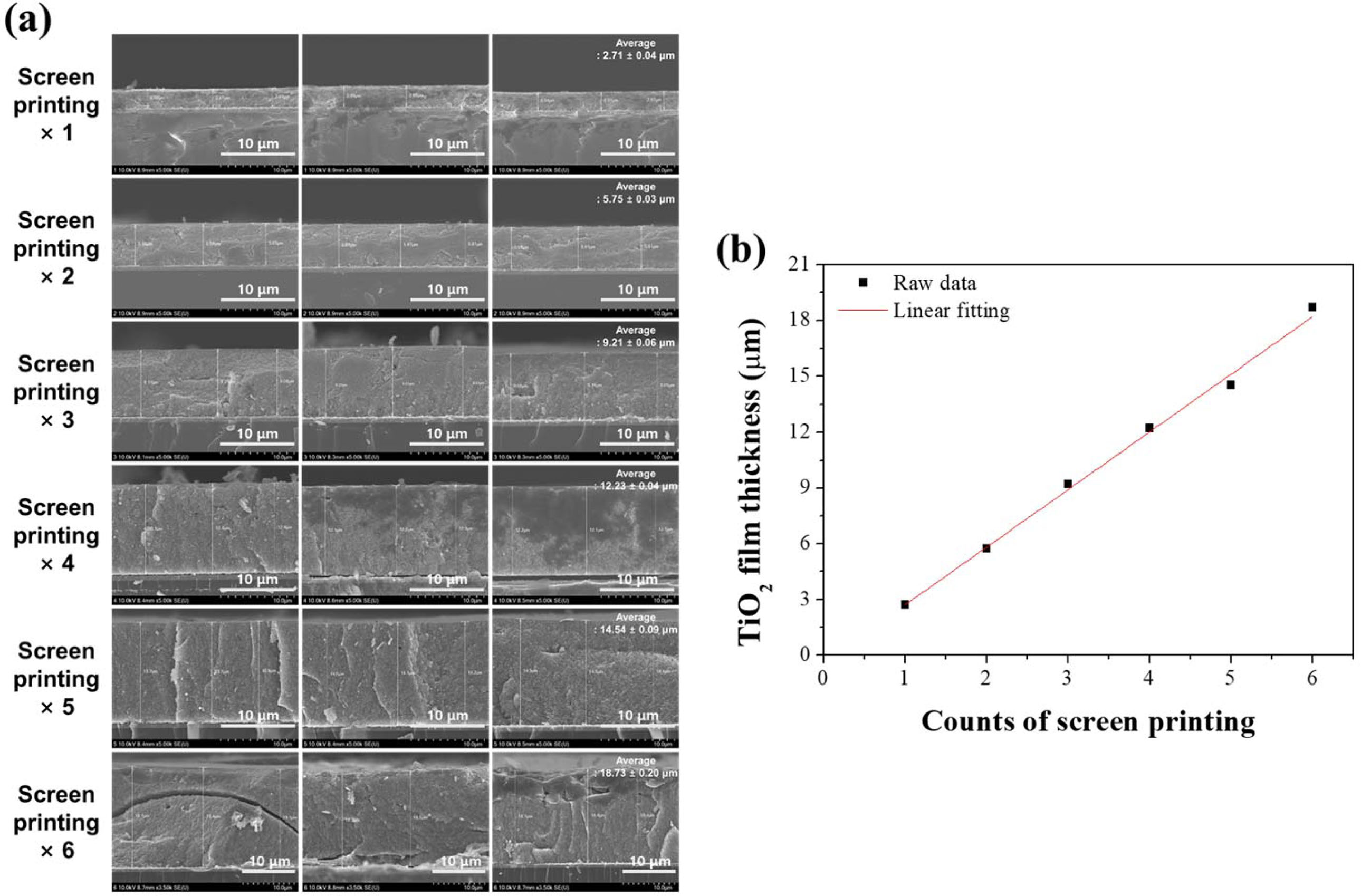
In the case of the screen printing process, the thickness of the film can be changed depending on the organic binder, particle size of the deposition materials constituting the paste, and the distance between the screen mask and substrate. The thickness of the TiO2 mesoporous film according to the number of screen printing cycles observed by HR-SEM is shown in Fig. 3(a). The thickness of the TiO2 films increased as the number of printings increased. Fig. 3(b) also shows the variation of thickness of the TiO2 films with screen printing. The thickness increases linearly by approximately 3 μm with each cycle.
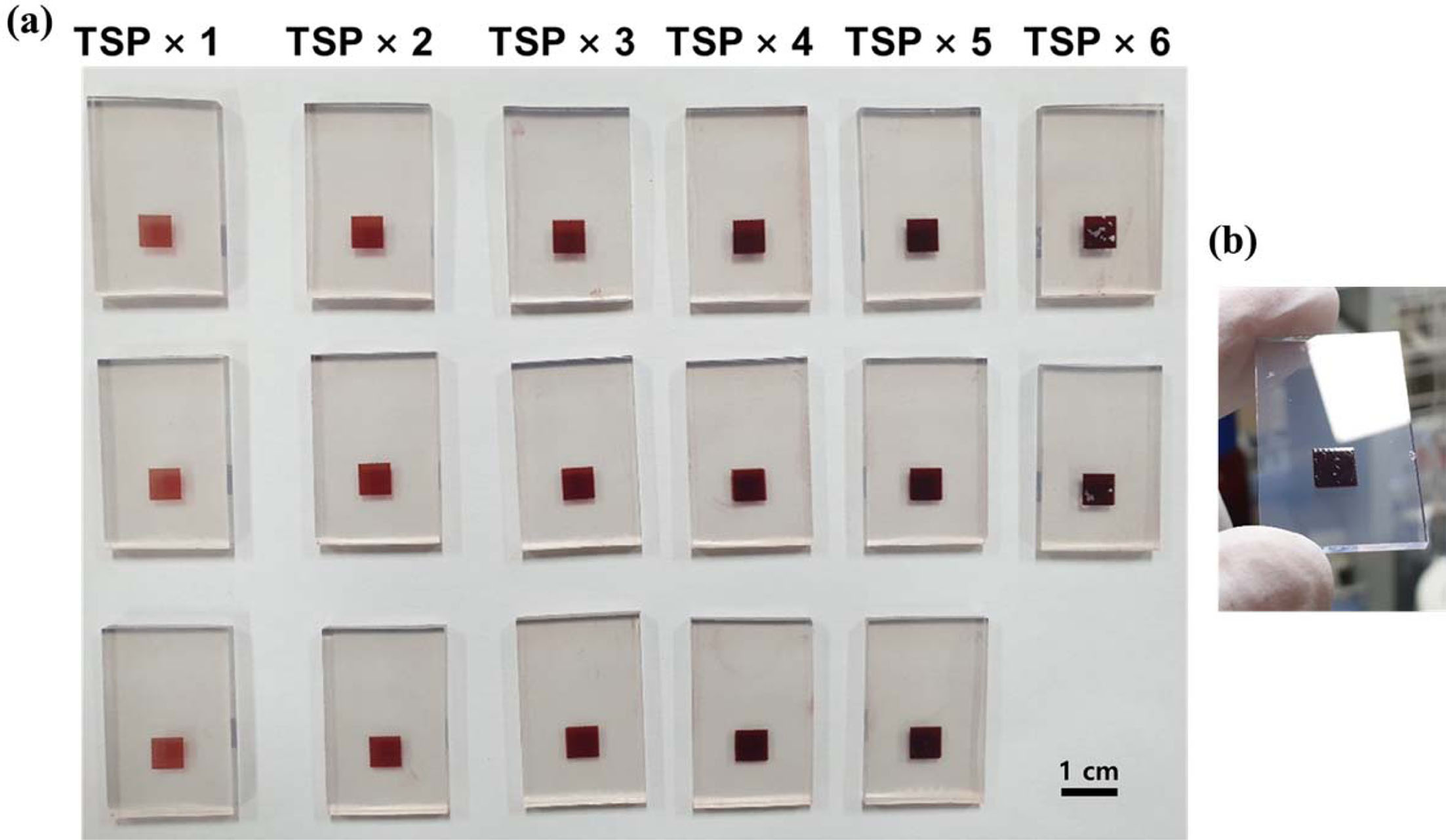
As shown in Fig. 4(a), the color of the film after the dye loading process became darker as the thickness of the TiO2 film increased. However, after five times screen printing (an approximately 12-μm thick film), a surface crack on the TiO2 film was observed. In the sample with 6 cycles of screen printing, parts of the TiO2 films were broken, as shown in Fig. 4(b).
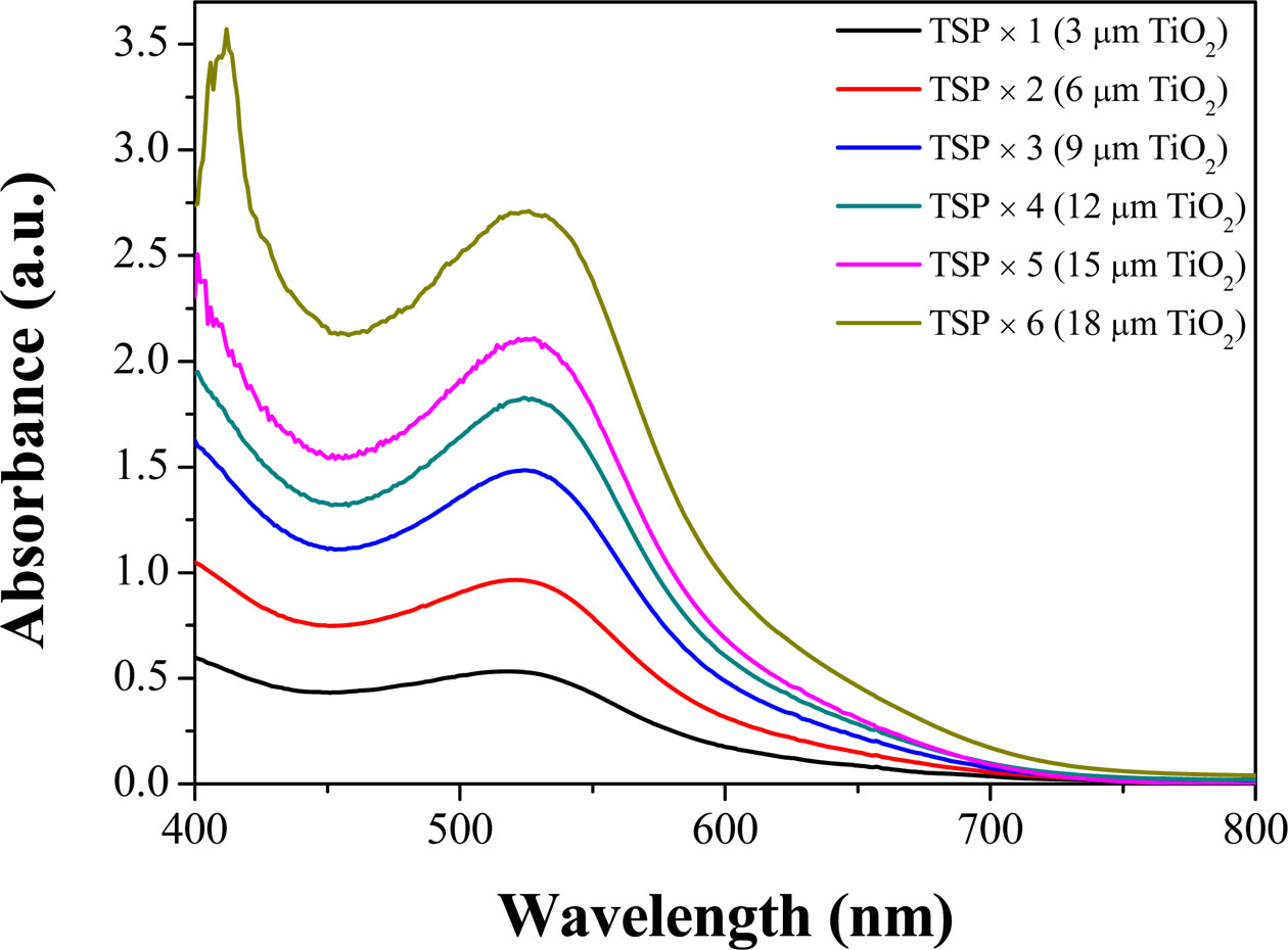
UV-visible spectroscopy analysis was performed to confirm the change in the adsorption amount of the N719 dye according to the change in the thickness of the TiO2 photoelectrode (Fig. 5). Similar to the color change tendency in Fig. 4, the absorbance in the 525-535 nm wavelength range had a tendency to increase as the thickness of the TiO2 photoelectrode increased [23, 24]. Therefore, the amount of dye adsorption increased by increasing the TiO2 mesoporous film thickness.
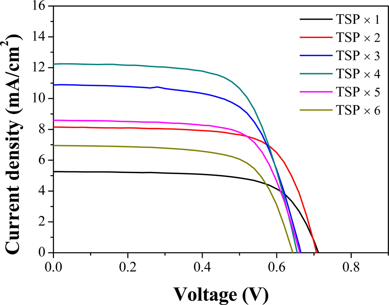
I–V characteristic measurements were performed to confirm the performance according to the change in the thickness of mesoporous TiO2 films and the parameters are listed in Table 1. As shown in Fig. 6, the efficiency increases as the thickness increases for up to 4 screen printing cycles. Noticeably, the current density increases with increasing thickness corresponding to the tendency of efficiency. The increase in the concentration of electron generation is because of the increase in the adsorption amount of the dye as the TiO2 thickness increases, resulting in an increase in Fermi level in the TiO2 conduction band, following an increase in current density with up to four screen printing cycles (12-μm thick). However, after four cycles printing, the perfor- mance of DSSC tended to decrease. According to the previous studies, the DSSC performance decreased when the photoelectrode had a critical thickness because of the reduced light transmittance and increased recom- bination, leading to a reduction in the electron generation and current density [25,26]. However, in this study, surface cracks were observed in the samples with a thickness of 15 μm (five screen printing cycles) and 18 μm (6 screen printing cycles), as shown in Fig. 3 and Fig. 4(b). The decrease in current density and performance after the fourth screen printing cycle is attributed to the surface crack generated when the deposition is too thick. The VOC has a tendency to decrease gradually as the thickness increased because the TiO2 photoelectrode creates a surface trap level on the TiO2 surface, resulting in an increase in the recombination with the electrolyte and consequent reduction in the VOC [22, 27]. Moreover, our results demonstrate that the obtained performances are comparable with several literatures [28-31] (Table 1).
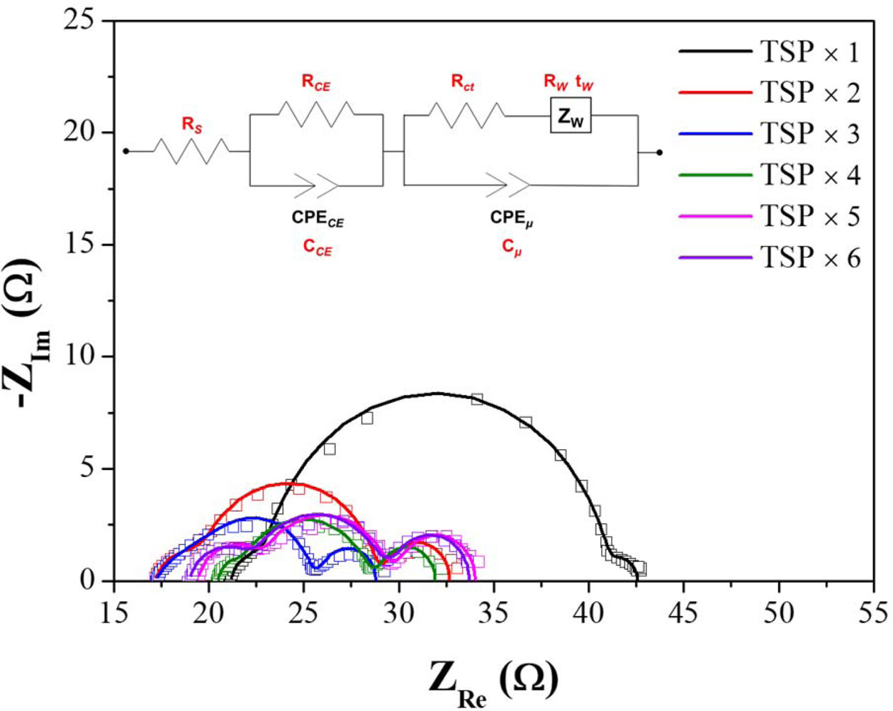
EIS was performed to confirm the electrochemical change in the DSSC according to the thickness change of the TiO2 films. Fig. 7 shows the Nyquist plots of the electrochemical impedance spectra of the DSSC for changing the thickness of the TiO2 photoelectrode. In a conventional DSSC, the three semicircles are drawn on the Nyquist plot in EIS data, which is designated to a redox reaction of 3I−/I3− at the Pt counter electrode (the first semicircle in the high frequency range), charge transfer reaction at the interface between TiO2/N719 and electrolyte (the second semicircle in the middle frequency range), and the Warburg diffusion process of iodide (the third semicircle in the low frequency range) [27, 32]. The electrochemical parameters obtained by the simulation of fitting between equivalent circuit and impedance spectra are listed in Table 2. The measured impedance data (dots) are well matched with the modeling data (lines) calculated by the equivalent circuit and electrochemical parameters. As shown in Fig. 7 and Table 2, the resistance of the charge transfer reaction in the TiO2/dye-electrolyte interface decreased as the thickness of TiO2 increased up to a thickness of 12 μm, and increased at thicker TiO2. This result is consistent with the tendency of the current density and efficiency in I–V characteristics. Alternative to the tendency of the charge transfer resistance, the capacitance of the charge transfer increases up to a thickness of 12 μm and then decreases at thicker TiO2. The tendency of impedance parameters in changing the thickness of the TiO2 is in agreement with previous studies in that one of the factors that increases the performance as the thickness increases is an increase in current density because of a decrease in charge transfer resistance, and the increase in charge transfer capacitance is related to the total density of electrons [32-34].
|
Fig. 3 (a) HR-SEM images and (b) thickness change of the TiO2 film deposited by 1–6 cycles of screen printing. |
|
Fig. 4 Images of the (a) TiO2 film color change according to cycles of screen printing after dye loading process and (b) TSP×5 film to show a crack on the TiO2 surface. |
|
Fig. 5 UV-visible spectroscopy of N719-absorbed TiO2/FTO/ Glass according to the changes in TiO2 photoelectrode thickness (Blank: TiO2 film/FTO/Glass). |
|
Fig. 6 Photocurrent density-voltage curves of DSSCs with the TiO2 film thickness change. |
|
Fig. 7 AC impedance spectra of DSSCs according to the TiO2 film thickness change (Dot: Raw data, Line: fitting data from equivalent circuit). |
|
Table 1 Short-circuit current (ISC), open-circuit voltage (VOC), maximum power, fill factor (FF), and power-conversion efficiency (η) of the DSSCs according to the TiO2 film thickness change. |
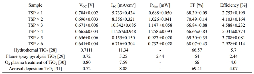
*The analysis results of I-V curve are the averages of at least 6 individual cells |
|
Table 2 Electrochemical resistance and capacitance of illuminated DSSCs of the TiO2 photoelectrode according to TiO2 film thickness change under open circuit conditions. Data were obtained from EIS fits using the equivalent circuits in Fig. 7. |
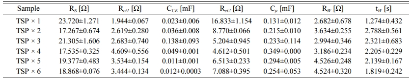
TiO2 mesoporous films were fabricated using a screen printing method with thickness of 3 μm/screen prints as determined by FE-SEM. As the thickness of TiO2 films increased to 12 μm, the performance of the DSSCs increased. I–V measurements showed the highest efficiency in the 12-μm thick film. The increase in overall performance may be because of the increase in current density (ISC: 11.267 mA/cm2 in the 12 μm TiO2 films). However, the efficiency tends to decrease with TiO2 thicker than 12 μm. The EIS demonstrated that the resistance of the TiO2/dye-electrolyte charge transfer reaction corresponding to the second semicircle in the Nyquist plot decreases up to a thickness of 12 μm and then increases, which is consistent with the tendency in I–V measurements. As the thickness of the TiO2 film increases, more current was generated because of an increase in the amount of dye loading, resulting in an increase in the performance. As the thickness increases, the amount of dye loading increased; however, the DSSC performance decreased at TiO2 thicker than 12 μm. This performance decrease was attributed to the connection break among TiO2 particles by surface cracking caused by stress differences between FTO/TiO2 and the TiO2 particle interface.
This research was supported by “Research Base Construction Fund Support Program” funded by Jeonbuk National University in 2020. This work was supported by the National Research Foundation of Korea (NRF) grant funded by the Korea government (MSIT) (No. 2018R1A4A1025528). This work was also supported by the Technology Development Program to Solve Climate Changes of the National Research Foundation (NRF) grant funded by the Korea government (Ministry of Science and ICT) (2017M1A2A2044930).
- 1. B. O'Regan and M. Grätzel, Nature 353[6346] (1991) 737-740.
-

- 2. P. Ramasamy, M.-S. Kang, H.-J. Cha, J. Kim, Mater. Res. Bull. 48[1] (2013) 79-83.
-
- 3. L. Zhao, J. Yu, J. Fan, P. Zhai, S. Wang, Electrochem. Commun. 11[10] (2009) 2052-2055.
-
- 4. S.K. Park, C. Chung, D.-H. Kim, C. Kim, S.-J. Lee, Y.S. Han, Mater. Res. Bull. 47[10] (2012) 2722-2725.
-
- 5. M. Gratzel. Nature 414[6861] (2001) 338-344.
-
- 6. K. Patil, S. Rashidi, H. Wang, W. Wei, Int. J. Photoenergy 2019 (2019) Article ID 1812879.
-
- 7. J.H. Kim, K.J. Lee, J.H. Roh, S.W. Song, J.H. Park, I.H. Yer, B.M. Moon, Nano. Res. Lett. 7 (2012)1-12.
- 8. M.U. Rahman, M. Wei, F. Xie, M. Khan, Catalysts 9[3] (2019) 273.
-
- 9. R. Kasaudhan, H. Elbohy, S. Sigdel, H. Qiao, Q. Wei, Q. Qiao, IEEE Electron Device Lett. 35[5] (2014) 578-580.
-
- 10. P. Sanjay, I. Isaivani, K. Deepa, J. Madhavan, S. Senthil, Mater. Lett. 244 (2019) 142-146.
-
- 11. R. Vittal, K.-C. Ho, Renewable Sustainable Energy Rev. 70 (2017) 920-935.
-
- 12. N.I. Beedri, P.K. Baviskar, V.P. Bhalekar, C.V. Jagtap, Inamuddin, A.M. Asiri, S.R. Jadkar, H.M. Pathan, Phys. Status Solidi A 215[18] (201) 1800236.
- 13. J.-J. Lee, M.M. Rahman, S. Sarker, N.C.D. Nath, A.J.S. Ahammad, J.K. Lee, Adv. Compos. Mater. Med. Nanotechnol. 182 (2011) 210-218.
- 14. S.N.F. Zainudin, H. Abdullah, M. Markom, J. Mater. Sci. 30[6] (2019) 5342-5356.
-
- 15. B. Roose, S. Pathak, U. Steiner, Chem. Soc. Rev. 44[22] (2015) 8326-8349.
-
- 16. C.C. Raj, R. Prasanth, J. Power Sources 317 (2016) 120-132.
-
- 17. H.-W. Lin, Y.-S. Wang, Z.-Y. Huang, Y.-M. Lin, C.-W. Chen, S.-H. Yang, K.-L. Wu, Y. Chi, S.-H. Liu, P.-T. Chou, Phys. Chem. Chem. Phys. 14[41] (2012) 14190-14195.
-
- 18. J.A. Anta, F. Casanueva, G. Oskam, J. Phys. Chem. B 110[11] (2006) 5372-5378.
-
- 19. K.-M. Lee, V. Suryanarayanan, K.-C. Ho, Sol. Energy Mater. Sol. Cells 90[15] (2006) 2398-2404.
-
- 20. K. Zhu, N. Kopidakis, N.R. Neale, J. van de Lagemaat, A.J. Frank, J. Phys. Chem. B 110[50] (2006) 25174-25180.
-
- 21. K. Zhu, S.-R. Jang, A.J. Frank, J. Phys. Chem. Lett. 2[9] (2011) 1070-1076.
-
- 22. S.R. Raga, E.M. Barea, F. Fabregat-Santiago, J. Phys. Chem. Lett. 3[12] (2012) 1629-1634.
-
- 23. P. Wen, Y. Han, W. Zhao, Int. J. Photoenergy 2012 (2012) Article ID 906198.
-
- 24. F. De Angelis, S. Fantacci, E. Mosconi, M.K. Nazeeruddin, M. Grätzel, J. Phys. Chem. C 115[17] (2011) 8825-8831.
-
- 25. V. Baglio, M. Girolamo, V. Antonucci, A.S. Aricò, Int. J. Electrochem. Sci 6[8] (2011) 3375-3384.
- 26. M.G. Kang, K.S. Ryu, S.H. Chang, N.G. Park, J.S. Hong, K.-J. Kim, Bull. Korean Chem. Soc. 25[5] (2004) 742-744.
-
- 27. S. Nakade, M. Matsuda, S. Kambe, Y. Saito, T. Kitamura, T. Sakata, Y. Wada, H. Mori, S. Yanagida, J. Phys. Chem. B 106[39] (2002) 10004-10010.
-
- 28. S.N. Karthick, K.V. Hemalatha, C.J. Raj, H.-J. Kim, M. Yi, J. Ceram. Proc. Res. 13[S1] (2012) 136-139.
- 29. A. Aboulouard, B. Gultekin, M. Can, M. Erol, A. Jouaiti, B. Elhadadi, C. Zafer, S. Demic, J. Mat. Res. Tech. 9[2] (2020) 1569-1577.
-
- 30. Y. Kim, B.J. Yoo, R. Vittal, Y. Lee, N.-G. Park, K.-J. Kim, J. Power Sources 175[2] (2008) 914-919.
-
- 31. D. Kim, K. Lee, H. Lee, J. Lim, J. Park, J. Kor. Cryst. Growth and Cryst. Tech. 30[2] (2020) 61-65.
-
- 32. J. Bisquert, M. Grätzel, Q. Wang, F. Fabregat-Santiago, J. Phys. Chem. B 110[23] (2006) 11284-11290.
-
- 33. J. Bisquert, J. Phys. Chem. B 106[2] (2002) 325-333.
-
- 34. F. Fabregat-Santiago, J. Bisquert, E. Palomares, L. Otero, D. Kuang, S.M. Zakeeruddin, M. Grätzel, J. Physic. Chem. C 111[17] (2007) 6550-6560.
-
 This Article
-
2021; 22(5): 584-589
Published on Oct 31, 2021
- 10.36410/jcpr.2021.22.5.584
- Received on May 7, 2021
- Revised on Jul 5, 2021
- Accepted on Jul 17, 2021
Services
- Abstract
introduction
experimental procedure
results and discussion
conclusions
- Acknowledgements
- References
- Full Text PDF
Shared
Correspondence to
- Ki-Tae Lee
-
aDivision of Advanced Materials Engineering, Jeonbuk National University, Jeonbuk 54896, Republic of Korea
bDepartment of Energy Storage/Conversion Engineering of Graduate School, Jeonbuk National University, Jeonbuk 54896, Republic of Korea
cHydrogen and Fuel Cell Research Center, Jeonbuk National University, Jeonbuk 54896, Republic of Korea
Tel : +82-63-270-2290 Fax: +82-63-270-2386 - E-mail: ktlee71@jbnu.ac.kr
Clean-Energy Research Institute(CRI), Hanyang University, 222, Wangsimni-ro, Seongdong-gu, Seoul, 04763, Korea
E-mail: jcpr@hanyang.ac.kr