


- Effect of thickness on moisture barrier properties of aluminum oxide using ozone-based atomic layer deposition
Juhyun Leea, Seokyoon Shina, Sejin Kwona, Woochool Janga, Hyeongsu Choia, Hyunwoo Parka, Namgue Leeb and Hyeongtag Jeona,b,*
aDivision of Materials Science and Engineering, Hanyang University, Seoul 04763, Korea
bDivision of Nanoscale Semiconductor Engineering, Hanyang University, Seoul 04763. KoreaThis article is an open access article distributed under the terms of the Creative Commons Attribution Non-Commercial License (http://creativecommons.org/licenses/by-nc/4.0) which permits unrestricted non-commercial use, distribution, and reproduction in any medium, provided the original work is properly cited.
Among various thin film encapsulation (TFE) methods, thin films prepared by atomic layer deposition (ALD) have been shown to provide superior protection against the permeation of moisture and oxygen. This technique has numerous of advantages such as excellent uniformity, precise thickness control, and strong adhesion. Therefore, with ozone-based ALD, we conducted the influence of the thickness of aluminum oxide (Al2O3) on moisture barrier properties. From the results of an electrical calcium test, Al2O3 had two distinctly different permeation regimes. Between 10 and 25 nm of Al2O3 thickness, the water vapor transmission rate (WVTR) decreased exponentially from 6.3 × 10⁻³ to 1.0 × 10⁻⁴ g m-2 day-1 (1/60 times). In contrast, as thickness increased from 25 to 100 nm, the WVTR values decreased by only two-thirds, from 1.0 × 10⁻⁴ to 6.6 × 10⁻⁵ g·m-2·day-1. To better understand the change from an exponential to a sub-exponential regime, defect density and refractive index of Al2O3 were measured. The thickness dependence on defect density and refractive index was analogous with one of moisture barrier performance. These results confirmed the existence of a critical thickness at which the WVTR decreased drastically
Keywords: Aluminum oxide, Ozone, Atomic layer deposition, Water vapor transmission rate
Organic light emitting diodes (OLEDs) are attractive due to their advantages, such as low voltage operation, mechanical flexibility, natural color reproduction, and ultra-thin structure [1-4]. Nevertheless, their vulnerability to water and oxygen is a major obstacle to commercial- ization of OLEDs. When organic devices are operated under ambient atmosphere, the formation of dark spots may result in their complete degradation [2]. For a stable device operation, OLEDs need an effective moisture permeation barrier with a water vapor transmission rate (WVTR) value on the order of 1 × 10⁻⁶ g·m-2·day-1 to guarantee a minimum lifetime of 10,000 h [3, 4]. A very common method to prevent oxidative species from entering organic devices is to encapsulate the device with a glass or metal lid. However, these encapsulation approaches with rigid materials have some problems in application in flexible electronics [4-6]. Therefore, development of an alternative encapsulation technique is required for future OLED devices.
Compared to other methods, thin film encapsulation (TFE) is a promising technique because it offers more flexible, lighter and thinner characteristics [3]. Commonly, it is performed using various low temperature deposition processes such as sputtering, plasma enhanced chemical vapor deposition (PECVD), and atomic layer deposition (ALD) [7-9]. Among various TFE methods, thin films prepared by ALD have been shown to provide superior protection against the permeation of moisture and oxygen [2]. This technique has numerous of advantages such as excellent uniformity, precise thickness control, and strong adhesion [10-12]. Above all, it can produce nearly defect-free thin films; thus, its thin films have been proposed as an ideal moisture barrier layer for passivating flexible electronics [13-16]. There are some examples in previous studies where the permeability of ALD thin films improved by orders of magnitude when a critical thickness was reached [10, 17, 18]. For aluminum oxide (Al2O3) processed by ALD [19, 20], critical thicknesses between 5 and 25 nm were found. It is obvious that the significant improvement in moisture barrier performance is strongly related to the thickness of ALD thin films. Furthermore, a critical thickness may be a key determinant in developing multi-layers of inorganic barrier layers and polymer-like interlayers.
In this work, we investigated thickness dependence on moisture barrier properties of Al2O3 prepared by ozone-based ALD. Al2O3 is one of most widely used insulating material due to its excellent dielectric properties, strong adhesion to dissimilar materials, and its thermal and chemical stabilities. It remains amorphous phase under typical processing conditions [21]. These properties make it an attractive candidate for the use in the field of flexible electronics. The Al2O3 thin films were deposited at a substrate temperature of 100 oC to minimize thermal sensitivity to the organic active layer of the OLED during deposition of the moisture barrier layer [4]. Trimethyl-aluminum (TMA), and ozone (O3) were used in thermal ALD experiments as aluminum (Al) precursors and oxygen reactants, respectively. With 10, 15, 20, 25, 50, and 100 nm thick Al2O3 samples, we conducted a systematic study of how WVTR values, defect densities, and refractive indices were influenced by thickness.
Al2O3 thin films were deposited at 100 oC using trimethylaluminum (TMA, Al(CH3)3) and ozone (O3) as aluminum and oxygen precursors, respectively. The series of Al2O3 thin films had thicknesses of 10, 15, 20, 25, 50, and 100 nm. The TMA precursor was placed in stainless-steel canister and maintained at room temperature during the deposition process. Argon (Ar) gas was used as purging gas and fixed at 200 sccm to maintain a process pressure of 0.55 Torr. All gas lines were heated at 100 oC. O3 was produced by an ozone generator (Sumitomo DL-1890B_SGRF-01DA) using oxygen (O2) gas and its concentration was maintained at 400 g/m3. The gas flow rate to the ALD chamber was fixed at 0.2 slm (standard liter per minute). Each ALD cycle consisted of a 1 s exposure of substrate to TMA vapor, 50 s of Ar purge to remove physisorbed TMA, a 3 s exposure to O3 gas, and then 30 s of Ar purge. The growth rate of Al2O3 was 1.2 Å/cycle, which was about the same as in our previous study [18]. Two types of substrates, p-type (100) silicon (Si) and polyethylenesulfone (PES), were prepared for Al2O3 thin film deposition. The Si substrates were cleaned with dilute hydrofluoric acid to remove oxide and other residues.
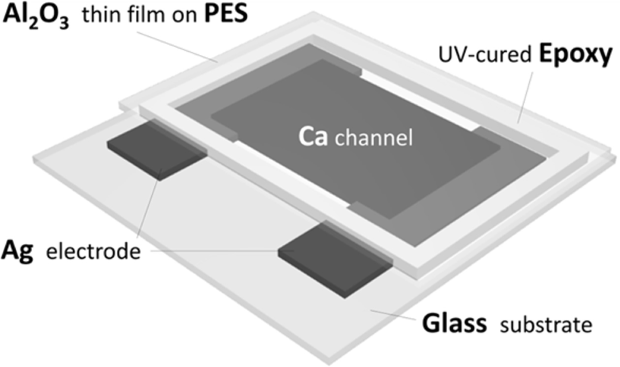
Thickness dependence on Al2O3 grown by the ozone-based ALD system was analyzed using various techniques. First, thickness and refractive index were measured by a spectroscopic ellipsometer (SE, M-2000V, J.A.WOOLLAM, Co., USA). Next, an electrical Ca test was performed to derive the WVTR of Al2O3 samples. Ca is a conductive material that easily reacts with oxidative species. Once Ca is oxidized, it becomes an insulator with high resistance. By monitoring the conductance change of Ca encapsulated by the moisture permeation barrier, it was possible to measure a maximum WVTR of 1 × 10⁻⁶ g·m-2·day-1. Fig. 1 is a schematic of an electrical Ca test sample for WVTR measurement. Ag electrodes with a thickness of 150 nm were deposited on a 5 × 5 cm2 glass substrate by an RF plasma sputter followed by a 1-μm-thick Ca deposition by thermal evaporation between the Ag electrodes by a shadow mask. The Al2O3 thin films on PES were sealed by a UV curable epoxy and the conductance change of Ca was monitored by I-V measurements in a thermos-hygrostat under controlled environment of 50 oC and 50% relative humidity (RH). Finally, the defect density was measured by the pinhole test. The pinhole test preparation was made by a 30% KOH (80 oC) etching attack on Si for 1 h, and then Al2O3 was etched with 10% HF (23 oC) for 10 min. Thereafter, the samples were immediately rinsed with deionized water to extirpate any residual contaminants. The defects created by this treatment were verified by field emission scanning electron microscopy (FESEM, JEOL-JSM 6330F).
|
Fig. 1 Schematic of the electrical Ca test sample for water vapor transmission rate measurement |
We measured the WVTR values to investigate the effect of Al2O3 thickness on moisture barrier properties. The WVTR measurement of Al2O3 samples with thicknesses of 10, 15, 20, 25, 50, and 100 nm were carried out by the electrical Ca test. Conductance changes of the Ca layer encapsulated with Al2O3 thin films as a function of water exposure time under accelerated condition (50 oC, 50% RH) are shown in the inset of Fig. 2. The slope of the conductance curve was used to calculate WVTR values according to the following equation:
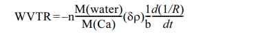
where n is the molar equivalent of the degradation reaction (n = 2 for water), and M(water) and M(Ca) represent the molar masses of the water (M(water) = 18 amu) and Ca (M(Ca) = 40.1 amu), respectively. δ corresponds to the density of Ca (δ = 1.55 g/cm3), ρ is the specific resistance of Ca (ρ = 3.4 × 10⁻⁸Ω m), and l (l = 2 cm) and b (b = 2 cm) are the length and width of the Ca layer, respectively [26, 27]. Using the slope of the conductance curve, WVTR can be calculated with thickness, density, width, and length of the Ca layer. As shown in Fig. 2, the calculated WVTR of Al2O3 with thicknesses of 10, 15, 20, 25, 50 and 100 nm were 6.3 × 10⁻³, 2.7 × 10⁻⁴, 1.5 × 10⁻⁴, 1.0 × 10⁻⁴, 8.0 × 10⁻⁵, and 6.6 × 10⁻⁵ g·m-2·day-1 at 50 oC and 50% RH, respectively. The moisture barrier performance of Al2O3 was signi- ficantly improved with increase in the thickness. In the thickness range of 10 to 25 nm, the WVTR decreased exponentially with increase of Al2O3 thickness. As the thickness of Al2O3 increased above 25 nm, a sub-exponential decrease of WVTR values was observed. Specifically, the WVTR decreased by 1/60 times for Al2O3 thickness 10 to 25 nm, while two thirds from for 25 to 100 nm. Namely, these results revealed that there was the change from an exponential to a sub-exponential permeation regime. In addition, Fig. 2(b) exhibits that our results are in line with the trend in WVTR of previous literatures, but the Al2O3 thin films deposited by our ALD system show relatively low WVTR values. Based on the above findings, additional analyses were carried out to study Al2O3 characteristics that affect moisture barrier properties with the increase in their thickness.
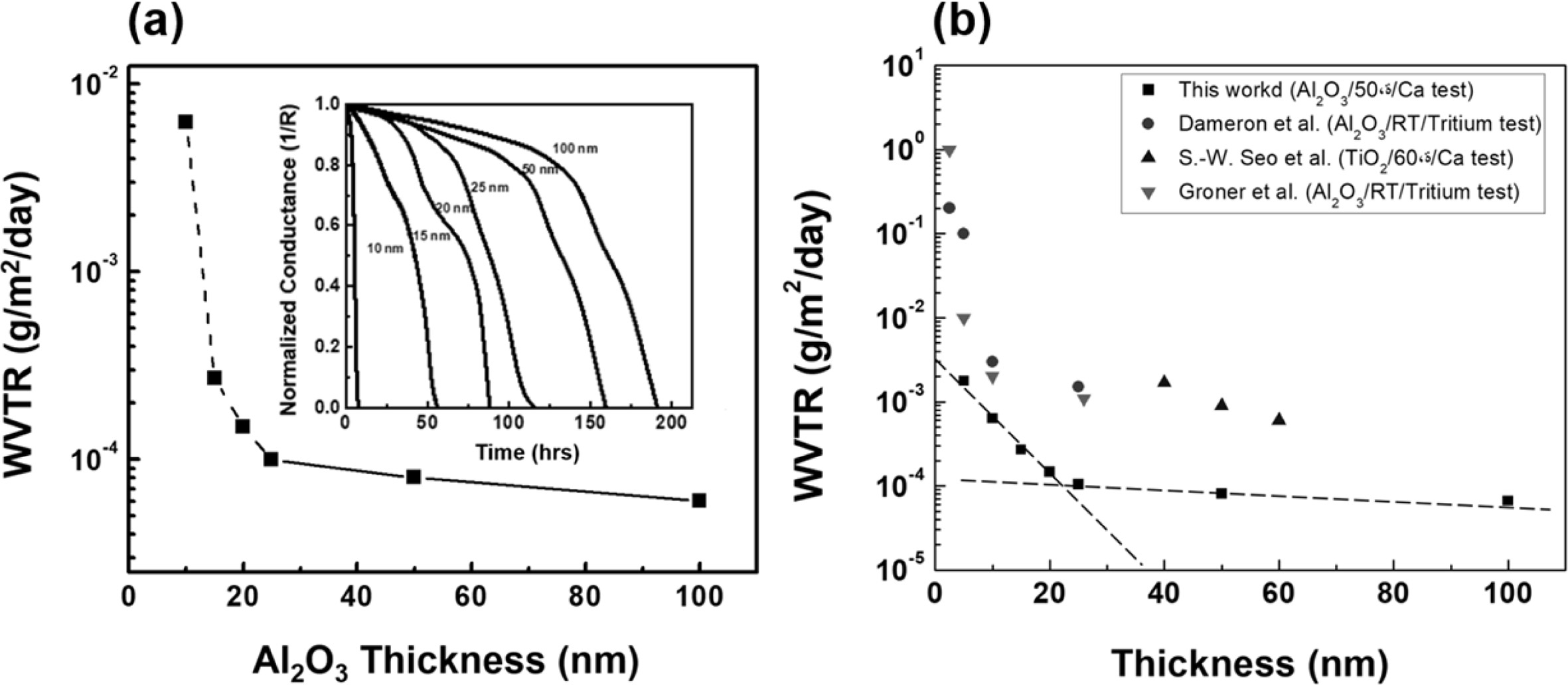
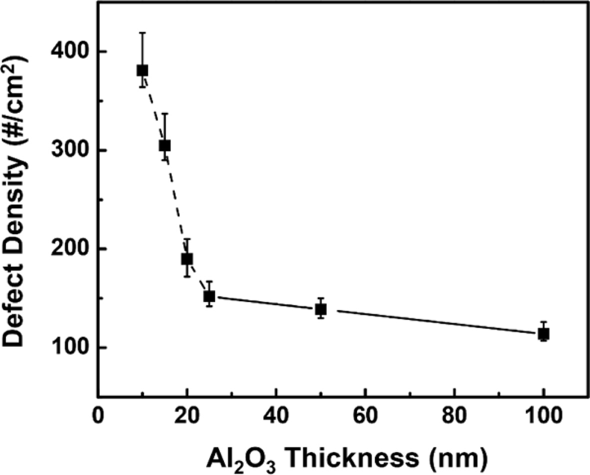
To analyze the relation between defects and moisture permeation barrier performance, the pinhole test and FESEM analysis were performed to determine the defect density. The defects in Al2O3 thin film were created by pinhole test. The Si substrate etching through defects of Al2O3 by KOH solution and Al2O3 thin film etching by HF solution was performed sequentially. Thereafter, the defect sites on Al2O3 were clearly observable in the FESEM image. Fig. 3 displays FESEM top view images of defect sites obtained on the areas of Al2O3 samples. In these images, it is found that with the increase in Al2O3 thickness, the number of defect sites decreased conspicuously. Water permeation has been universally found to occur unhindered through defects present in the moisture barrier layer, which may lead to a fast degradation of the OLEDs [28]. Therefore, decrease of defect sites brought about improvement of moisture permeation barrier as Al2O3 thickness increased. Fig. 4 also shows the variation in defect density as a function of the thickness. The calculated defect densities of samples prepared at the thickness of 10, 15, 20, 25, 50 and 100 nm were 381, 305, 190, 152, 139 and 114 #/cm2, respectively. The defect density decreased significantly in the thickness from10 to 25 nm, whereas it changed little above 25 nm. The self-limiting aspect of ALD leads to conformal deposition even on high aspect ratio structures, which can virtually cover most defects such as pinholes and particles [12]. Hence, a steep decline in defect density for Al2O3 thicknesses of up to 25 nm was caused by a reduction of and reinforcement of defect sites, resulting in the formation of a continuous moisture barrier layer. As samples thicker than 25 nm were past any critical thickness for continuous thin film formation, the reduction of rapid decrease in defect density was observed. This is similar to the trend in WVTR, which explains why the change from an exponential to a sub-exponential permeation regime is observed.
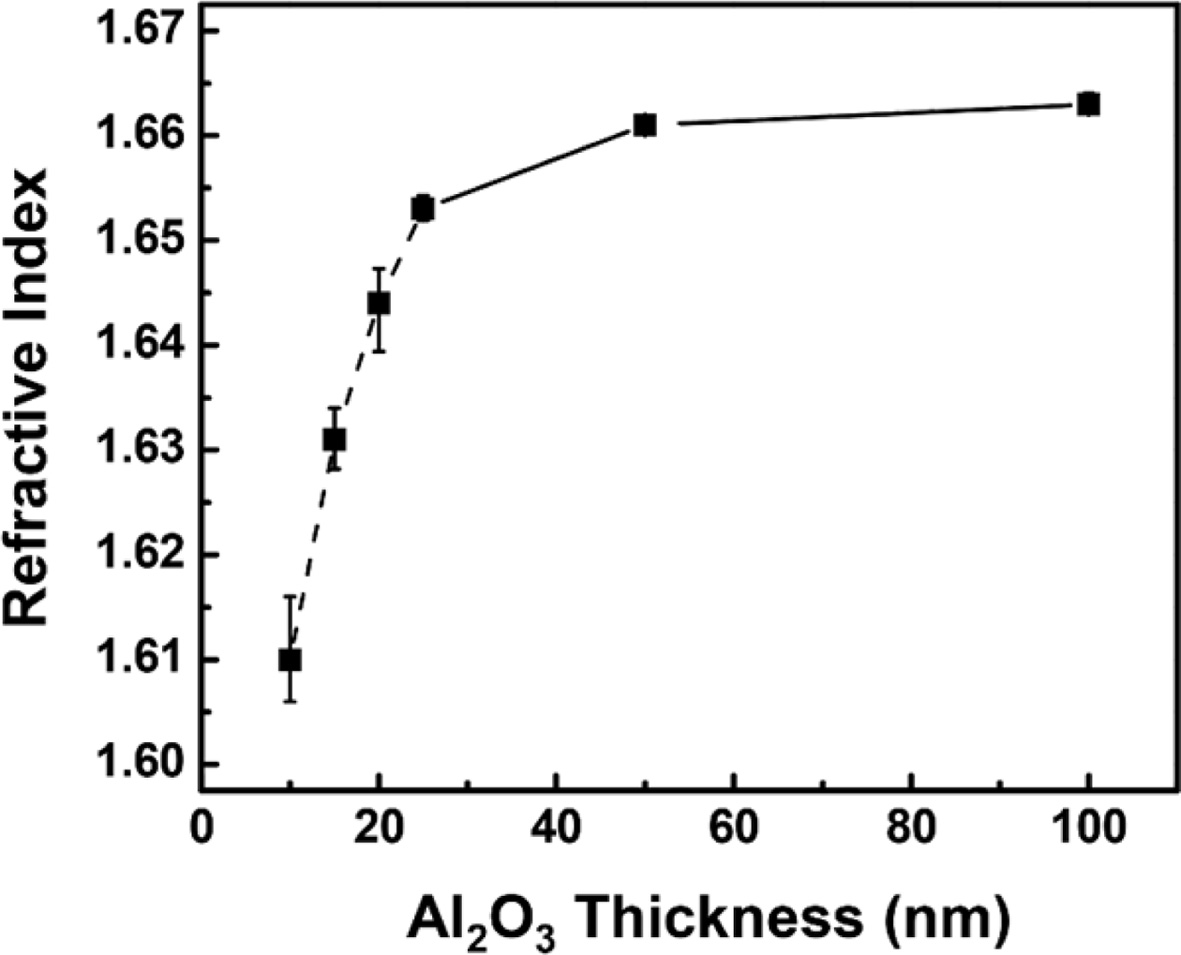
Generally, the moisture barrier performance of a thin film is influence by their physical properties, particularly its density. The density is a critical determinant of the refractive index because refractive index results from closely related to the collective response of electric dipoles excited by the external applied field and, the number of dipoles in a given volume is closely related to the density [29, 30]. Thus, the refractive index is considered as a proxy for assessing the physical pro- perties of a thin film. In order to analyze the physical properties of Al2O3, we carried out the refractive index measurement using SE. Fig. 5 shows the refractive index of Al2O3 samples as a function of thickness. At thicknesses of 10, 15, 20, 25, 50, and 100 nm, the refractive indices were 1.61, 1.63, 1.64, 1.65, 1.66, and 1.66, respectively. Between 10 and 25 nm, the measured refractive indices of the Al2O3 thin films changed from 1.61 to 1.65. However, there was no change in the refractive indices of the Al2O3 samples with the thickness above 25 nm. The moisture barrier layer with relatively high WVTR has a relatively low refractive index, which indicates that a majority of defect sites such as pinholes exist in the thin films [9]. As a consequence, as the thickness of Al2O3 thin films increased, the decrease in defect density made them denser, which was the reason for the improvement in moisture barrier performance.
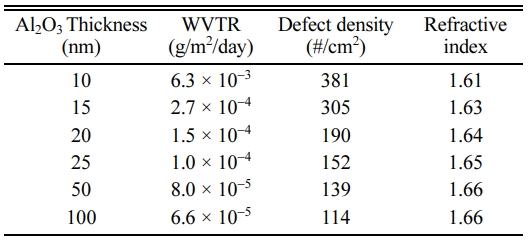
The above-mentioned results are summarized in Table 1. These results indicated the existence of critical thickness, at which the change from an exponential to a sub-exponential permeation regime was observed. The dependence of moisture barrier performance and Al2O3 thickness had a similar tendency with the defect density and refractive index. In Al2O3 thickness below 25 nm, the significant improvement of moisture barrier properties resulted from rapid decrease in defect sites, which related to the increase in refractive index. In contrast, the gradual decrease in WVTR value of samples with the thickness above 25 nm had relevance to little change in the defect density and refractive index. That’s to say, we interpret the improvement of moisture permeation performance as the formation of continuous thin films by a reduction of defect sites with the increase of Al2O3 thickness. Hence, for the production of an appropriate moisture permeation barrier with Al2O3, the number of ALD cycles is important to reduce the defect sites and increase the refractive index.
|
Fig. 2 (a) WVTR curves of Al2O3 thin film with the thicknesses of 10, 15, 20, 25, 50, and 100 nm at 50% and 50% RH. (b) Comparison of WVTR reported in previous literatures. |
|
Fig. 3 FESEM top view images of defects in Al2O3 thin film with thickness of (a) 10 nm, (b) 15 nm, (c) 20nm, (d) 25 nm, (e) 50 nm, and (f) 100 nm, respectively. |
|
Fig. 4 Defect density variation according to Al2O3 thin film thicknesses. |
|
Fig. 5 Refractive index as a function of Al2O3 thin films thicknesses using spectroscopic ellipsometer. |
|
Table 1 WVTR, refractive index and defect density comparison of Al2O3 thin films with thicknesses of 10, 15, 20, 25, 50 and 100 nm |
We investigated the thickness dependence on moisture barrier properties of Al2O3 thin films deposited by ozone-based ALD at relatively low temperature (100 oC) in order to optimize the thickness of Al2O3 as a moisture permeation barrier. This work was performed with Al2O3 thin films with thickness of 10, 15, 20, 25, 50, and 100 nm. The moisture barrier performance had two distinctively different permeation regime. Between 10 and 25 nm, the calculated WVTR decreased exponentially. By contrast, samples with thickness above 25 nm showed a sub-exponential decrease of WVTR. In order to find out a cause of this transition, the defect density and refractive index of Al2O3 samples were analyzed using the pinhole test (defect density) and a SE measurement (refractive index), respectively. A significant improvement of moisture barrier layer with thickness up to 25 nm resulted from reduction of the defect density and increase of refractive index. Whereas, the samples with a thickness series ranging from 25 to 100 nm had the saturation of WVTR value, defect density, and refractive index. We confirmed the existence of a critical thickness of Al2O3 deposited by ozone-based ALD. Based on these results, further studies should focus on the improvement of thin film properties in order to achieve a WVTR on the 1 × 10⁻⁶ g·m-2·day-1, which is applied to the optimization of moisture barrier properties for future flexible OLED encapsulation.
This research was supported by the MOTIE (Ministry of Trade, Industry & Energy, No. 20010604) and KSRC (Korea Semiconductor Research Consortium) support program for the development of the future semiconductor device.
Juhyun Lee and Seokyoon Shin contributed equally to this work.
- 1. S.-H.K. Park, J. Oh, C.-S. Hwang, J.-I. Lee, Y.S. Yang, and H.Y. Chu, Electrochem. Solid State Lett. 8 (2005) H21-H23.
-

- 2. S. Shin, H. Choi, G. Ham, J. Park, J. Lee, H. Choi, S. Lee, H. Kim, and H. Jeon, J. Vac. Sci. Technol. A 35 (2017) 021514.
-
- 3. J.-S. Park, H. Chae, H.K. Chung, and S.I. Lee, Semicond. Sci. Technol. 26 (2011) 034001.
-
- 4. A.P. Ghosh, L.J. Gerenser, C.M. Jarman, and J.E. Fornalik, Appl. Phys. Lett. 86 (2005) 223503.
-
- 5. P.F. Carcia, R.S. McLean, M.H. Reilly, M.D. Groner, and S.M. George, Appl. Phys. Lett. 89 (2006) 031915.
-
- 6. J.S. Lewis and M.S. Weaver, IEEE J. Sel. Top. Quantum Electron. 10 (2004) 45-57.
-
- 7. A.G. Erlat, B.M. Henry, C.R.M. Grovenor, A.G.D. Briggs, R.J. Chater, and Y. Tsukhara, J. Phys. Chem. B 108 (2004) 883-890.
-
- 8. P.F. Carcia, R.S. McLean, M.D. Groner, A.A. Dameron, and S.M. George, J. Appl. Phys. 106 (2009) 23533.
-
- 9. H. Jung, H. Jeon, H. Choi, G. Ham, S. Shin, and H. Jeon, J. Appl. Phys. 115 (2014) 073502.
-
- 10. E. Langereis, M. Creatore, S.B.S. Heil, M.C.M. van de Sanden, and W.M.M. Kessels, Appl. Phys. Lett. 89 (2006) 081915.
-
- 11. S.M. George, Chem. Rev. 110 (2010) 111-131.
-
- 12. S. Shin, G. Ham, H. Jeon, J. Park, W. Jang, and H. Jeon, Korean J. Mater. Res. 23 (2013) 405-422.
-
- 13. S.-W. Seo, E. Jung, C. Lim, H. Chae, and S.M. Cho, Appl. Phys. Exp. 5 (2012) 035701.
-
- 14. M.D. Groner, F.H. Fabreguette, J.W. Elam, and S.M. George, Chem. Mater. 16 (2004) 639-645.
-
- 15. A.A. Dameron, S.D. Davidson, B.B. Burton, P.F. Carcia, R.S. McLean, and S.M. George, J. Phys. Chem. C 112 (2008) 45734580.
-
- 16. K.-L. Jarvis, and P.-J. Evans, Thin Solid Films. 624 (2017) 111.
-
- 17. A.S. da Silva Sobrinho, G. Czeremuszkin, M. Latrèche, and M.R. Wertheimer, J. Vac. Sci. Technol. A 18 (2000) 149-157.
-
- 18. M.D. Groner, S.M. George, R.S. McLean, and P.F. Carcia, Appl. Phys. Lett. 88 (2006) 051907.
-
- 19. S. Jakschik, U. Schroeder, T. Hecht, M. Gutsche, H. Seidl, and J.W. Bartha, Thin Solid Films. 425[1-2] (2003) 216-220.
-
- 20. A. Cappella, J.-L. Battaglia, V. Schick, A. Kusiak, A. Lamperti, and C. Wiemer, B. Hay, Adv. Eng. Mater. 15[11] (2013) 1046-1050.
-
- 21. H. Choi, S. Shin, H. Jeon, Y. Choi, J. Kim, S. Kim, S.C. Chung, and K. Oh, J. Vac. Sci. Technol. A. 34 (2016) 01A121.
-
- 22. P.F. Carcia, R.S. McLean, and M.H. Reilly, Appl. Phys. Lett. 97 (2010) 221901.
-
- 23. J. Meyer, H. Schmidt, W. Kowalsky, T. Riedl, and A. Kahn, Appl. Phys. Lett. 96 (2010) 243308.
-
- 24. Z. Zhu, P. Sippola, H. Lipsanen, H. Savin, and S. Merdes, Jpn. J. Appl. Phys. 57 (2018) 125502.
-
- 25. J. Oh, S. Shin, J. Park, G. Ham, and H. Jeon, Thin solid films 599 (2016) 119-124.
-
- 26. R. Paetzold, A. Winnacker, D. Henseler, V. Cesari, and K. Heuser, Rev. Sci. Instrum. 74 (2003) 5147-5150.
-
- 27. S. Schubert, H. Klumbies, L. Müller-Meskamp, and K. Leo, Rev. Sci. Instrum. 82 (2011) 094101.
-
- 28. A.-M. Andringa, A. Perrotta, K. de Peuter, H.C.M. Knoops, W.M.M. Kessels, and M. Creatore, ACS Appl. Mater. Interfaces. 7 (2015) 22525-22532.
-
- 29. Y. Liu and P.H. Daum, J. Aerosol Sci. 39 (2008) 974-986.
-
- 30. Y. Etinger-Geller, A. Katsman, and B. Pokroy, Chem. Mater. 29 (2017) 4912.
-
 This Article
-
2021; 22(3): 253-257
Published on Jun 30, 2021
- 10.36410/jcpr.2021.22.3.253
- Received on May 1, 2019
- Revised on Jan 4, 2021
- Accepted on Apr 21, 2021
Services
- Abstract
introduction
experimental
results and discussion
conclusion
- Acknowledgements
- Author Contributions
- References
- Full Text PDF
Shared
Correspondence to
- Hyeongtag Jeon
-
aDivision of Materials Science and Engineering, Hanyang University, Seoul 04763, Korea
bDivision of Nanoscale Semiconductor Engineering, Hanyang University, Seoul 04763. Korea
Tel : +82-2-2220-0387 Fax: +82-2-2292-3523 - E-mail: hjeon@hanyang.ac.kr
Clean-Energy Research Institute(CRI), Hanyang University, 222, Wangsimni-ro, Seongdong-gu, Seoul, 04763, Korea
E-mail: jcpr@hanyang.ac.kr