


- Electrocaloric effect in heterolayered potassium tantalate niobate thin films prepared by sol-gel method
Byeong-Jun Parka,†, Sam-Haeng Leeb,c,†, Ji-Won Kimb, Joo-Seok Parkc and Sung-Gap Leeb,*
aDept. of Ceramic Engineering, Gyeongsang National University, Jinju 52828, Republic of Korea
bDept. of Materials Engineering and Convergence Technology, RIGET, Gyeongsang National University, JinJu 52828, Republic of Korea
cBusiness Cooperation Center, Korea Institute of Ceramic Engineering and Technology, Jinju 52851, Republic of KoreaThis article is an open access article distributed under the terms of the Creative Commons Attribution Non-Commercial License (http://creativecommons.org/licenses/by-nc/4.0) which permits unrestricted non-commercial use, distribution, and reproduction in any medium, provided the original work is properly cited.
Heterolayered potassium tantalate niobate(KTN(70/30)/KTN(30/70)) thin films on Pt/Ti/SiO2/Si substrates prepared by the sol-gel process and spin coating method. When sintered at 700 oC or higher, the X-ray diffraction intensities of the perovskite phase were greatly increased, and it was observed as the main phase of the KTN heterolayered thin film. As the sintering temperature increased from 650 oC to 800 oC, the average grain size increased from 146nm to 380 nm, and the average thickness of the KTN films coated six times was about 394-441 nm. Dielectric constant and dielectric loss of the KTN film sintered at 750 oC and room temperature showed good properties of about 2850 and 0.573, respectively, and all films exhibited the typical dielectric relaxation characteristics. The phase transition temperature of KTN thin film was around 12-13 oC. Remanent polarization and the coercive field of KTN film sintered at 750 oC showed excellent properties of 23.98 μC/cm2 and 35.41 kV/cm, respectively. Adiabatic temperature changes (ΔT) and electrocaloric strength of the KTN films sintered at 750 oC at 60 oC were 2.67 oC and 0.012 KcmkV-1, respectively
Keywords: Potassium tantalite niobate, Electrocaloric effect, Thin film, Solgel method
When an electric field is applied to a ferroelectric material under adiabatic condition, the entropy and temperature in the material changes with the change of polarization, and this is known as the electrocaloric effect (ECE) [1]. The ECE has high energy efficiency, and has the advantage of being eco-friendly. It is expected to be applied as a potential alternative cooling device for small electronic devices and parts. Reversible adiabatic temperature change (ΔT), due to the applied field ΔE, is calculated from the following equation [2]:
where, C is the specific heat, ρ is the density, E1 is the start electric field, E2 is the final electric field, and (∂P⁄∂T) is the pyroelectric coefficient, respectively. Indirect measurement of the ΔT are often based on Eq. (1).
Considerable EC effects (ΔT = 12 K) in PZT (95/5) thin film was reported [3] and many studies on ECE materials and devices have been conducted.
However, PZT-based ferroelectric materials exhibiting excellent EC effects are difficult to use at room temperature because their Curie temperature is higher than 240 oC.
Ferroelectrirc KTN (KTa1-xNbx)O3) material with perovskite crystal structure is well known as a ferroelectric material with an excellent electro-optical effect [4,5]. Additionally, Curie temperature depends on the composition ratio of Ta and Nb, and varies from 0K for KTN(100/0) to 710 K for KTN(0/100) [6]. Therefore, KTN is attracting attention as an ECE material because it is possible to adjust the phase transition temperature to around room temperature by controlling the composition ratio of KTaO3 and KNbO3.
In previous studies, we investigated the structural and electrical properties of Pb(Zr1-xTix)/Pb(ZrxTi1-x) and Pb(Zr,Ti)O3/BiFeO3 heterolayered thin films in which films of different compositions and crystal structures are alternately stacked. It was observed that the structural and ferroelectric properties of the heterolayered films improved as the lower layer affected the crystallization of the upper layer during the annealing process [7,8]. In this study, in order to fabricate KTN heterolayered thin film having a phase transition temperature near room temperature, KTN(30/70) film and KTN(70/30) film having cubic and orthorhombic crystal structures, re- spectively, were alternately stacked. Remanent polarization and coercive field for KTN heterolayered thin films are higher than those of single composition KTN (65/35) and KTN (73/27) films. Also, structural and electrical properties according to the sintering temperature were observed in order to investigate the possibility of application to Pb-free EC material.
All reactions and manipulations were carried out under dry nitrogen using a glove box and standard Schlenk techniques. The process of this synthesis is similar to our previous report [9]. KTN precursor solutions were fabricated using tantalum ethoxide (C10H25TaO5), niobium ethoxide (C10H25NbO5) and potassium ethoxide (KOCH2CH3) as raw materials, similarly as in Ref. [9]. 2-Methoxyethanol (CH3OCH2CH2OH) was selected as the solvent. 10 mol% of excess potassium ethoxide was added to compensate for the expected alkali losses during the heating of the films. In the process of thin films, dusts and impurities were removed firstly from the solution by a 0.3 μm syringe filter. KTN heterolayered thin films were grown on Pt/Ti/SiO2/Si substrates by spin coating method. First, KTN (70/30) solution was deposited on the substrate, and then was dried at 200 oC for 5 min. After, it was pre-annealed at 400 oC for 15 min to pyrolyze the residual organic compounds. KTN (30/70) solution was deposited on the obtained KTN (70/30) film and dried then pre-annealed under the same conditions. This process was repeated 6 times, and the KTN heterolayered thin film was fabricated with sintering time and temperature of 650~800 oC and 1h, respectively. In order to observe the structural characteristics of KTN heterolayered films, X-ray diffraction analysis and microstructure were observed. Using film ferroelectric tester RT-66B (Radiant Tech. USA), polarization-electric field (P-E) hysteresis properties according to temperature and applied electric field were observed. The possibility of application as EC devices was investigated.
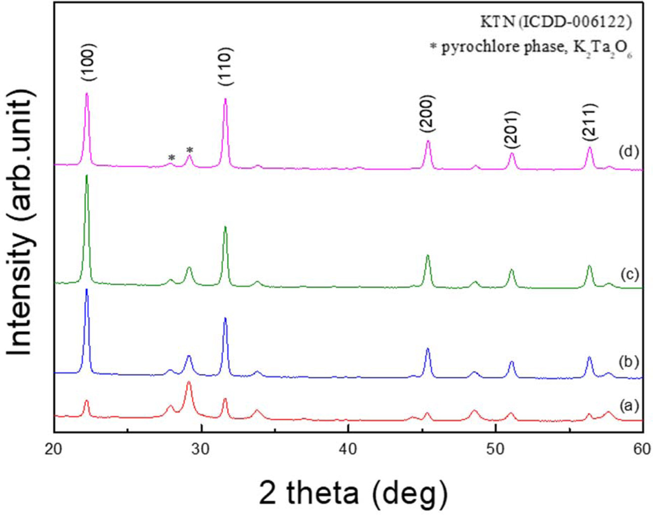
Fig. 1 shows the X-ray diffraction patterns with variation of the sintering temperature of the KTN heterolayered thin film. As the sintering temperature increased from 650 oC to 800 oC, it was observed that the intensities of X-ray diffraction peaks and FWHM (full width at half maximum) decreased, thereby improving the crystallinity. K2Ta2O5 pyrochlore phase near the diffraction angle 2θ = 29o showed a tendency to decrease with an increase in the sintering temperature, but was also observed in the specimen sintered at 800 oC. In the KTN films sintered at 650 oC, the pyrochlore phase was observed as a major phase, however, above 700 oC, the diffraction intensities of the perovskite phase increased significantly and was observed as a major phase. In general, the pyrochlore phase is crystallized at a lower temperature than the perovskite phase, and the pyrochlore phase has a stable oxide crystal structure at room temperature. It also does not change into a perovskite phase or disappear completely even when the sintering temperature increases. Although not shown in this paper, KTN films sintered at 850 oC which is the K-deficient pyrochlore phase, their composition might be Ta2O5 · nKTaO3 (n = 2, 3, 4) (ASTM 12-92, 31-1098, 21-687), rapidly increased due to volatilization of K ions. KTN (30/70) and KTN (70/30) materials have orthorhombic and cubic structures at room temperature, respectively [10]. However, all KTN heterolayered thin films showed a polycrystalline crystal structure with no preferred orientation, which is because the lower KTN films with different crystal structures influenced the crystallization of the upper films during the annealing process.
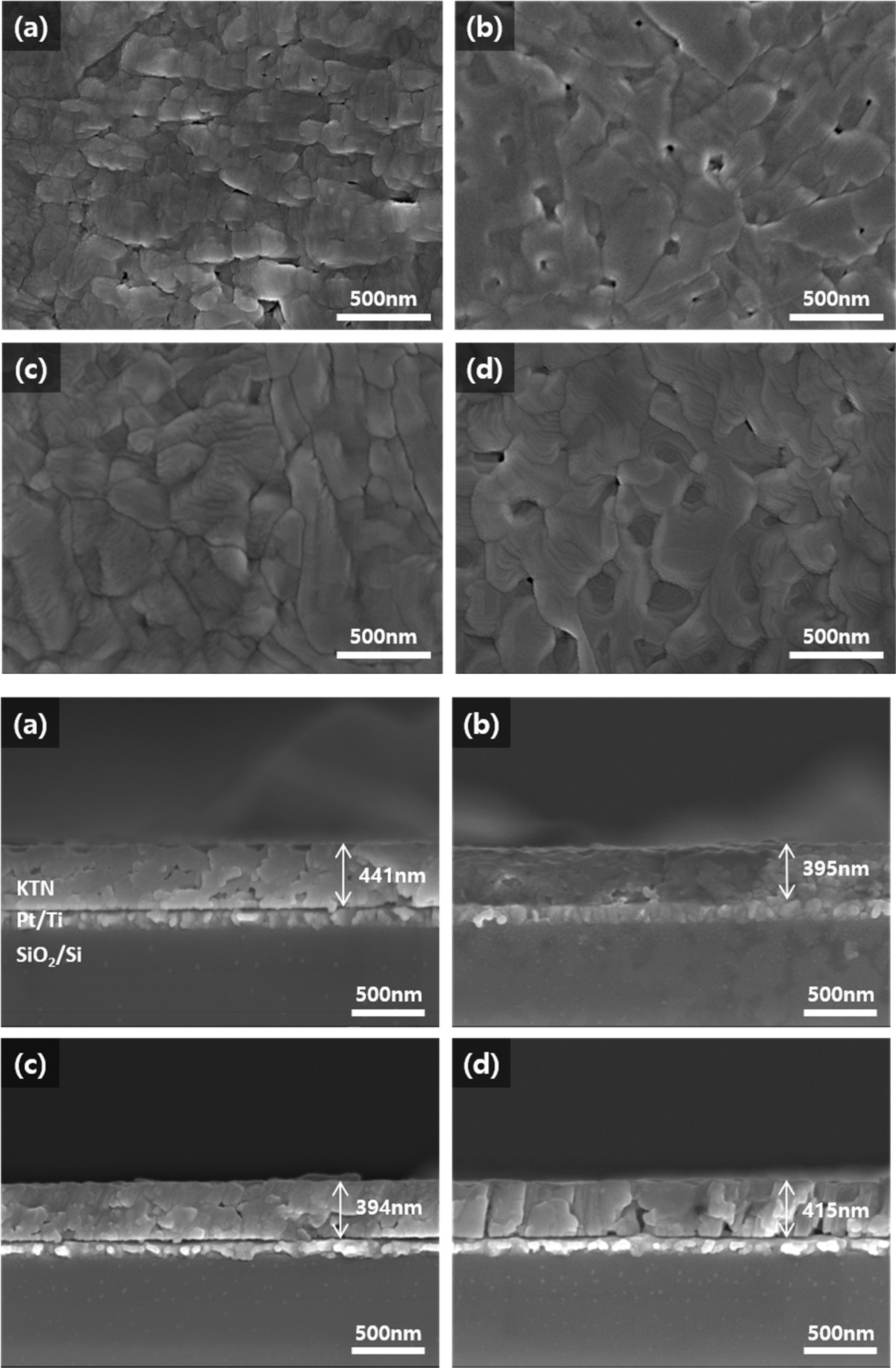
Fig. 2 shows surface and cross-sectional microstructure with variation of sintering temperature of the KTN heterolayered thin film. As the sintering temperature increased from 650 oC to 800 oC, the average grain size increased from 146nm to 380nm, and showed a dense structure. However, in the case of the films sintered at 650 oC and 800 oC, some pores were observed, which is thought to be due to incomplete grain growth due to the low sintering temperature and volatilization of K-ions due to excessive sintering temperature, respectively. Average thickness of KTN films was about 394-441 nm and showed a uniform and flat cross-sectional structure. Interface between KTN (30/70) films and KTN (70/30) films could not be observed, which is believed to be due to the small heterogeneity between the interfaces due to the same crystalline structure and same K, Nb, Ta constituent elements.
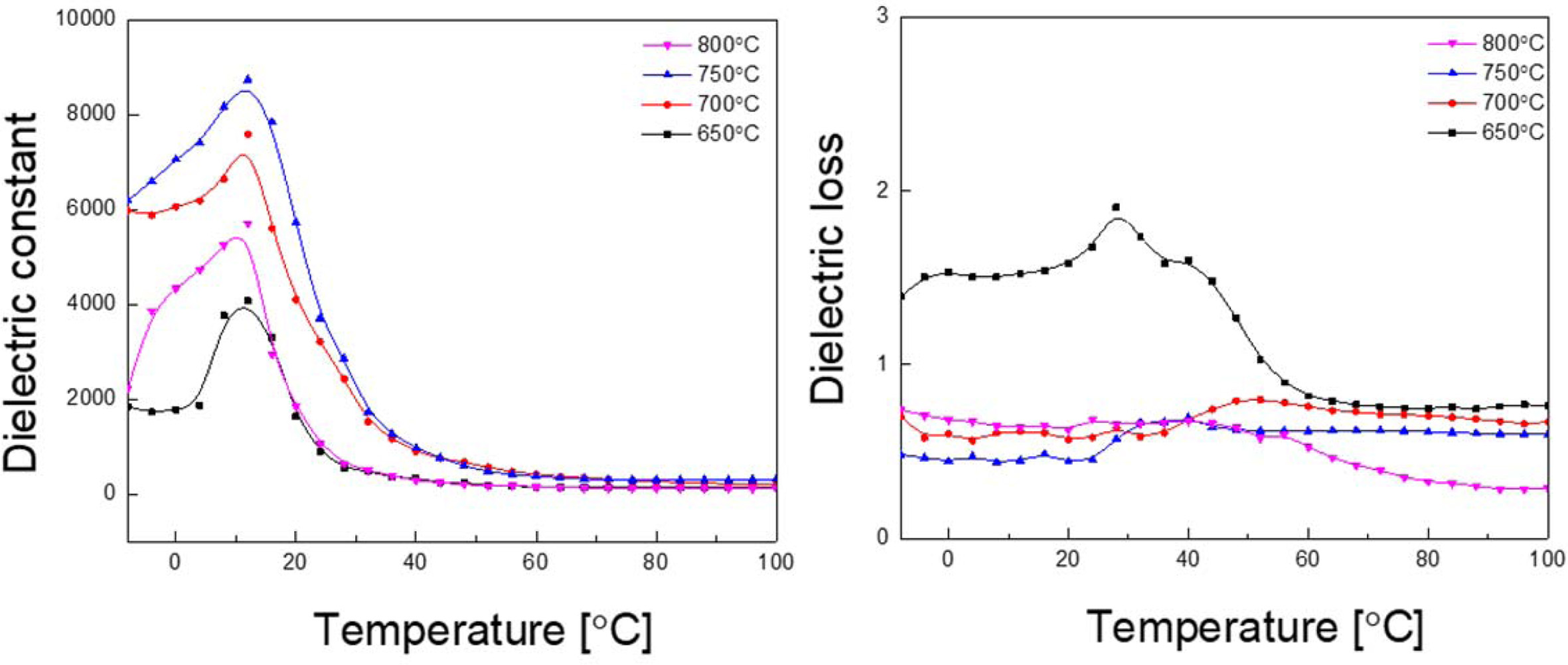
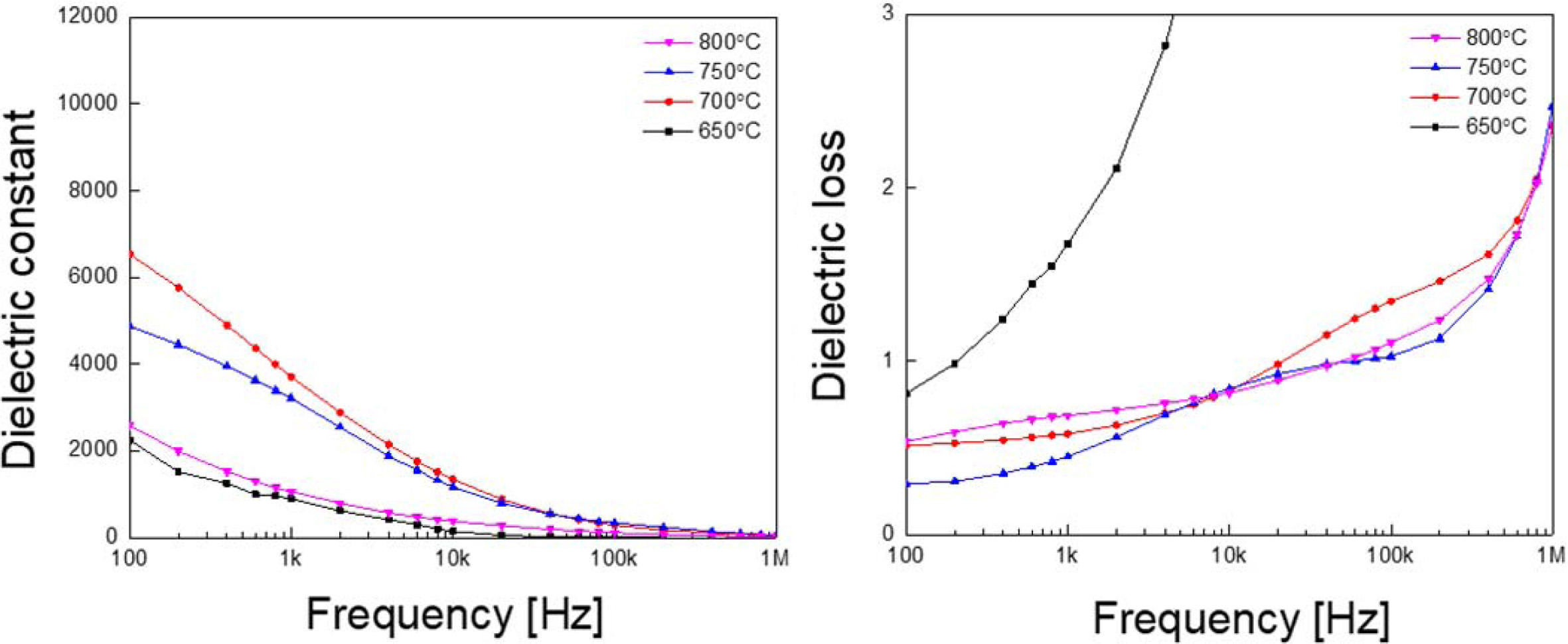
Fig. 3 shows relative dielectric constant and dielectric loss with variation of temperature of KTN heterolayered films. Dielectric constant increased with increasing the sintering temperature, showing the highest value in the film sintered at 750 oC before decreasing at 800 oC. This is because the pyrochlore phase and pores decreased, and the ferroelectric grain size increased with the increase in sintering temperature, as observed in Fig. 1 and 2. Curie temperatures of KTN (30/70) and KTN (70/30) materials are 230 oC and –25 oC, respectively [11]. However, KTN heterolayered films fabricated in our study exhibited a phase transition temperature of about 12-13 oC. This is because thin films with different structural and electrical properties are repeatedly stacked together, so that the lower layer affects the crystallization of the upper layer when the specimen is sintered. It is believed to be due to the formation of the interfacial layers due to the diffusion of Ta and Nb ions [12]. KTN films sintered at 650 oC exhibited high dielectric loss due to the distribution of the pyrochlore phase and the formation of an incomplete crystal phase. Dielectric constant and dielectric loss at room temperature of the KTN films sintered at 750 oC were about 2,850 and 0.573, respectively.
Fig. 4 shows dielectric constant and dielectric loss according to the frequency of KTN heterolayered films. All KTN films exhibited typical dielectric relaxation characteristics in which the dielectric constant decreases as the frequency increases, and, the dielectric constant decreased significantly in the high frequency region. This is thought to be due to the formation of space charge polarization due to the diffusion of ions and lattice mismatch at each interface as the heterolayered structure was fabricated using KTN films with different compositions ratio and crystal structures [12].
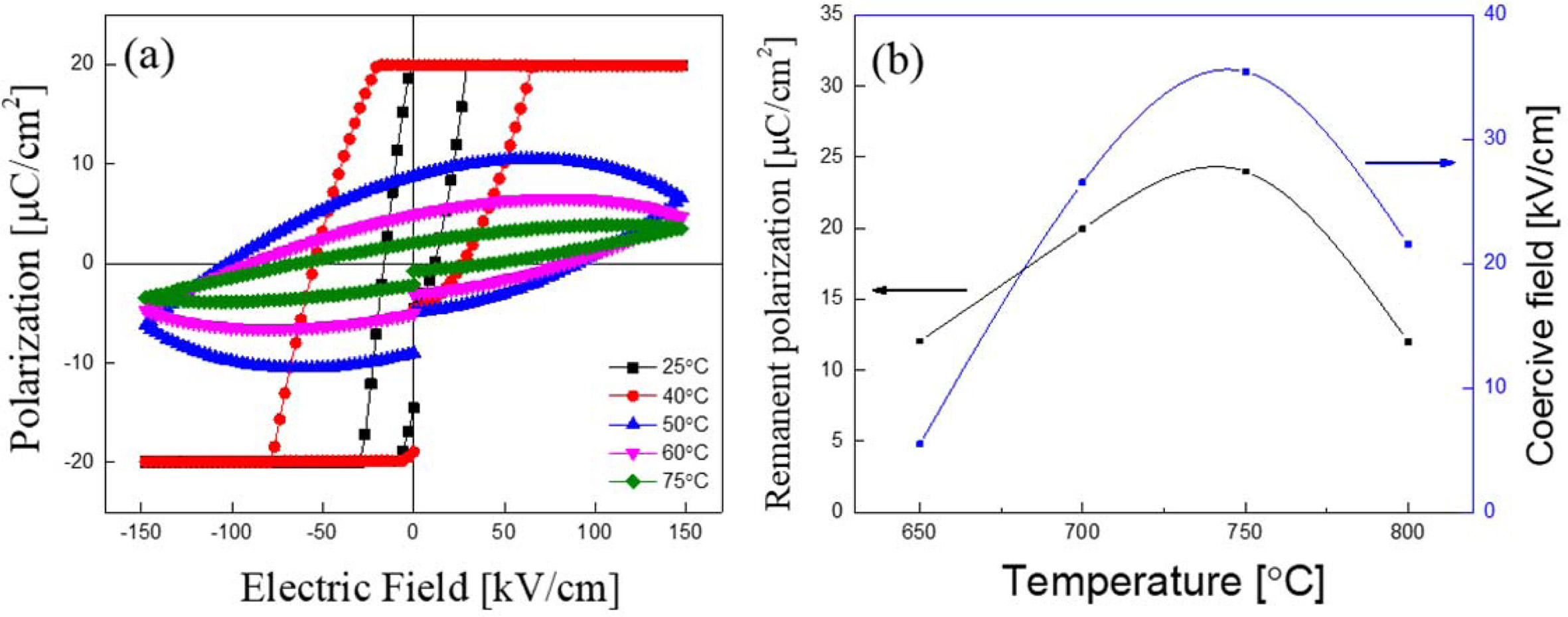
Fig. 5(a) shows P-E hysteresis loop and 5(b) shows remanent polarization and coercive field with a variation of the sintering temperatures of KTN heterolayered film sintered at 700 oC. Remanent polarization and coercive field increased as sintering temperature increased and showed a maximum value in the KTN film sintered at 750 oC. These properties are due to the decrease of the pyrochlore phase and the increase of average grain size due to an increase of the sintering temperature. The ferroelectric properties of KTN films sintered at 800 oC decreased due to the formation of depolarizing field by pores. Also, remanent polarization and coercive field for KTN heterolayered thin films are higher than those of single composition KTN(65/35) (Pr = 2.8 μC/cm2, Ec = 5.0 kV/cm) and KTN(73/27) (Pr = 7.5 μC/cm2, Ec = 2.8 kV/cm) films [13, 14]. KTN heterolayered thin films sintered at 750 oC shows the remanent polarization of 23.98μC/cm2 and coercive field of 35.41kV/cm.
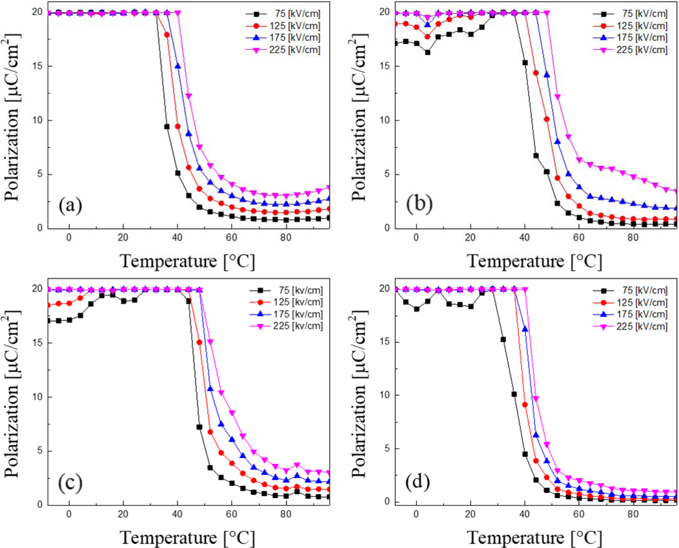
Fig. 6 shows remanent polarization of the KTN heterolayered films according to the temperature and applied electric field. As the applied electric field increases, the temperature at which the polarization decreases moved higher, which is believed to be because the applied DC electric field inhibits the switching of dipoles and induces the forced polarization arrangement. Under an electric field of 225 kV/cm, the temperature at which the polarization begins to decrease rapidly is about 40 oC in KTN films sintered at 650 oC and 800 oC, and at about 47 oC in KTN films sintered at 700 oC and 750 oC. As discussed in the structural characteristics, KTN films sintered at 650 oC and 800 oC exhibited a property of decreasing polarization at low temperatures because the formation of depolarizing field due to the pyrochlore phase and pores.
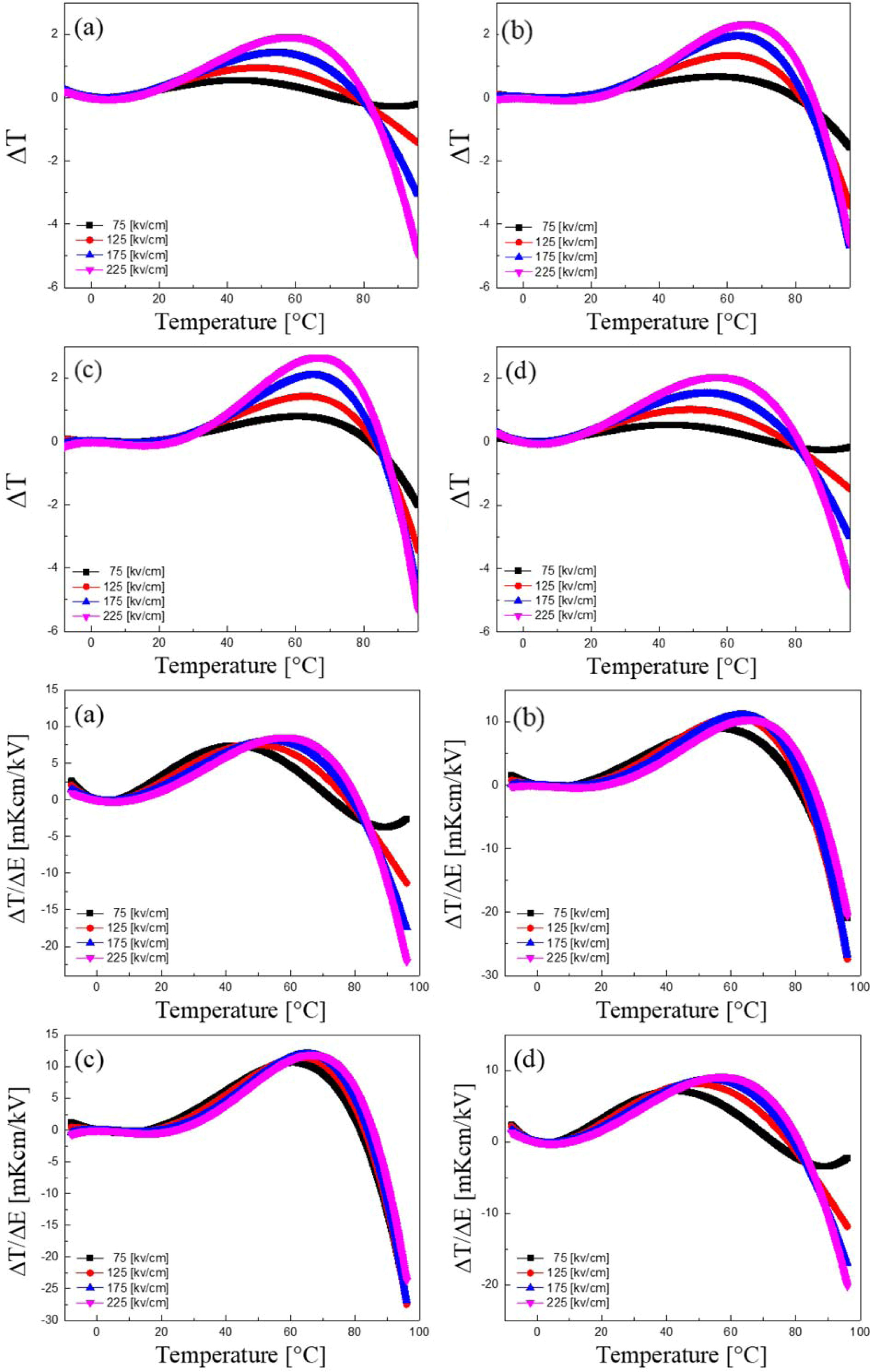
Fig. 7 shows the adiabatic temperature change (ΔT) of KTN heterolayered thin films with a variation of temperature. ΔT increased with an increasing of the sintering temperature, and the highest value, 2.67 oC, was obtained in the KTN film sintered at 750 oC. Furthermore, in all KTN films, the maximum ΔT values occurred at about 60-65 oC higher than the Curie temperature. This is because, at a slightly higher tempera- ture than the phase transition temperature, ferroelectric phase and paraelectric phase coexist and the dipole is easily switched by the application of the temperature and electric field. In general, in order to apply the electric caloric effect as a cooling element, an excellent electric caloric effect or an operation near room tem- perature is required. Usually excellent ΔT properties at near room temperature are required in order to apply the cooling devices. However, substantial EC properties have been observed in PZT-based materials having a high phase transition temperature of above 240 oC [3, 15]. But, EC strength (|ΔT/ΔE| [16]) of the KTN heterolayered film sintered at 750 oC was about 0.012 KcmkV-1 at 60 oC, which is almost two times larger than that (about 0.0064 KcmkV-1) obtained in BNT-0.1BT thin films at 50 oC [17]. Therefore, by controlling the interface characteristics and the applied field of KTN heterolayered thin films, we can get the giant EC coefficient at around room temperature, which may provide the potential for practical application.
|
Fig. 1 X-ray diffraction patterns with variation of the sintering temperature of the KTN heterolayered thin film |
|
Fig. 2 Surface and cross-sectional microstructure with variation of sintering temperature of the KTN heterolayered thin film. |
|
Fig. 3 Relative dielectric constant and dielectric loss with variation of temperature of KTN heterolayered films |
|
Fig. 4 Dielectric constant and dielectric loss according to the frequency of KTN heterolayered films. |
|
Fig. 5 (a) P-E hysteresis loop and (b) Remanent polarization and coercive field with a variation of the sintering temperatures of KTN heterolayered film sintered at 700 oC. |
|
Fig. 6 Remanent polarization of the KTN heterolayered films according to the temperature and applied electric field. |
|
Fig. 7 Adiabatic temperature change (ΔT) and Electrocaloric strength (|ΔT/ΔE|) of KTN heterolayered thin films with a variation of temperature. |
In summary, KTN heterolayered films were fabricated by alternately stacking KTN (30/70) and KTN (70/30) films having cubic and orthorhombic structures, respectively. In the KTN films sintered at 650 oC, the pyrochlore phase was observed as a major phase, however, above 700 oC, the diffraction intensities of the perovskite phase increased significantly and was observed as a major phase. KTN heterolayered thin films showed a polycrystalline crystal structure with no preferred orientation, which is thought to be because the lower KTN films with different crystal structures influenced the crystallization of the upper films during the annealing process. Also, remanent polarization and coercive field for KTN heterolayered thin films are higher than those of single composition KTN (65/35) and KTN (73/27) films. This is thought to be due to the formation of space charge polarization due to the diffusion of ions and lattice mismatch at each interface as the heterolayered structure was fabricated using KTN films with different compositions ratio and crystal structures. In all KTN films, the maximum ΔT values occurred at slightly higher temperature than the Curie temperature. This is believed to be because, at around this temperature, the ferroelectric phase and paraelectric phase coexist, and the dipole is easily switched by the application of the temperature and electric field.
This research was supported by Basic Science Research Program through the National Research Foundation of Korea (NRF) funded by the Ministry of Education (No. 2017R1D1A3 B03032164) and by Center for Women in Science, Engineering and Technology (WISET) grant funded by the Ministry of Science and ICT (MSIT) under the team research program for female engineering students (No. 202002190001).
- 1. B. Neese, B. Chu, S.-G Lu, Y. Wang, E. Furman and Q.M. Zhang, Science 321[5890} (2008) 821-823.
-

- 2. W. Geng, Y. Liu, X. Meng, L. Bellaiche, J.F. Scott, B. DKhkil and A. Jiang, Adv. Materials 27[20] (2015) 3165-3169.
-
- 3. A.S. Mischenko, Q. Zhang, J.F. Scott, R.W. Whatmore and N.D. Mathur, Science 311[5765] (2006) 1270-1271.
-
- 4. F.S. Chen, J.E. Geusic, S.K. Kurtz, J.G. Skinner and S.H. Wemple, J. Appl. Phys. 37[1] (1966) 388-398.
-
- 5. K. Nakamura, J. Miyazu, M. Sasaura and K. Fujiura, Appl. Phys. Lett. 89[13] (2006) 131115.
-
- 6. S. Triebwasser, Phys. Rev. 114[1] (1959) 63-70.
-
- 7. K.T. Kim, C.I. Kim and S.G. Lee, Microelectron. Eng. 66[1-4] (2003) 662-669.
-
- 8. S.H. Jo and S.G. Lee, J. Ceram. Proc. Res. 13[5] (2012) 631-634.
- 9. M.S. Kwon, S.G. Lee, and K.M. Kim, J. Ceram. Proc. Res. 19[4] (2018) 321-326.
- 10. K. Nakamura, J. Miyazu, Y. Sasaki, T. Imai, M. Sasaura and K. Fujura, J. Appl. Phys. 104[1] (2008) 013105.
-
- 11. B. Liu, X. Wang, Y. Zhang, X. Lv and Y. Yang, Ionics 20[12] (2014) 1795-1799.
-
- 12. M.R. Park, S.G. Lee, K.M. Kim, and K.S. Kwon, J. Ceram. Proc. Res. 18[6] (2017) 431-434.
- 13. S. Wang, Z. Li, D. Zhang, G. Zhang, J. Sun and D. Zheng, J. Sol-Gel Sci. and Tech. 17[2] (2000) 159-162.
-
- 14. H. Maiwa, Jap. J. Appl. Phys. 55[10S] (2016) 10TB09.
-
- 15. X.H. Hao, Z.X. Yue, J.B. Xu, S.L. An and C.W. Nan, J. Appl. Phys. 110[6] (2011) 064109.
-
- 16. X. Moya, E. Stern-Taulats, S. Grossley, D. Gonzalez-Alonso, S. Kar-Narayan, A. Planers. L. Manosa and J. D. Mathur, Adv. Mater. 25[9] (2013) 1360-1365.
-
- 17. X.C. Zheng, G.P. Zheng, Z. Lin and Z.Y. Jiang, Thin Solid Films 522 (2012), 125-128.
-
 This Article
-
2021; 22(2): 214-220
Published on Apr 30, 2021
- 10.36410/jcpr.2021.22.2.214
- Received on Sep 11, 2020
- Revised on Nov 3, 2020
- Accepted on Nov 11, 2020
Services
- Abstract
introduction
experimental
results and discussion
conclusions
- Acknowledgements
- References
- Full Text PDF
Shared
Correspondence to
- Sung-Gap Lee
-
Dept. of Materials Engineering and Convergence Technology, RIGET, Gyeongsang National University, JinJu 52828, Republic of Korea
Tel : +82-10-2686-4427 Fax: +82-55-772-1689 - E-mail: lsgap@gnu.ac.kr
Clean-Energy Research Institute(CRI), Hanyang University, 222, Wangsimni-ro, Seongdong-gu, Seoul, 04763, Korea
E-mail: jcpr@hanyang.ac.kr