


- ZnO nanorods-based piezoelectric nanogenerators on double-sided conducting paper
G M Hasan Ul Bannaa and Il-Kyu Parkb,*
aSchool of Mechanical and Electronic Engineering, East China University of Technology, Nanchang, Jiangxi, People’s Republic of China
bDepartment of Materials Science and Engineering, Seoul National University of Science and Technology, Seoul 01811, South Korea
We report on the voltage
output enhancement from ZnO nanorod (NR)-based bendable piezoelectric
nanogenerators (PENGs) with a conducting paper. Double-sided carbon paper
(DSCP) was used as a conducting substrate. Structural investigations by
scanning electron microscope and X-ray diffraction results showed that ZnO NRs
were successfully grown via a two-step hydrothermal process on both sides of
the CP. Photoluminescence peak intensity ratio of the band-edge to the deep
level emissions from the ZnO NRs on both sides of the CP substrate was similar
values in the range of 1.8 to 2, which indicating a similar crystalline quality
of the ZnO NRs on the front and back sides. The output characteristics from the
two PENG devices on the CP substrate showed identical piezoelectric output. The
output voltage from the DSCP-based PENG was 2.56- and 1.86-fold greater than
that from the single-sided PENG devices on only the front and back of the CP
substrate, respectively. This enhancement was attributed to the synergetic
effect between the PENGs on the front and back of CP and to the modification of
the CP’s electrical properties under an electric field generated by the PENGs
on the opposite side of the CP substrate.
Keywords: ZnO, Nanorods, Nanogenerator, Hydrothermal, Piezoelectricity
The increasing popularity of mobile and portable devices
for internet of things technologies has concen- trated research focus on potential
sustainable powering systems, including electrical energy scavenging from ubiquitous
ambient energy such as nuclear, mechanical, thermal, and electrochemical
energies. Transforming mechanical energy into electrical energy is a promising
avenue anytime and anywhere because of its abundant availability
in the human body and surrounding environ- ments, such as bodily fluid
movement, muscle stretching, mechanical
triggering, and airflow [1-5]. There are three energy conversion techniques
from mechanical sources based on triboelectric, electromagnetic, and piezoelectric
principles [6]. And piezoelectric energy harvesting has attracted strong
attention for energy harvesting ever since the first demonstration
of a one-dimensional nano- structure-based
piezoelectric nanogenerator (PENG) in 2006 and the subsequent improvements in
performance for practical applications [5-14].
Among the piezoelectric materials for self-powering PENG
applications, ZnO has become the most popular due to its adaptability to a wide
variety of substrates, such as silicon, sapphire, metal sheet, and conducting papers
for fabricating nanostructures [10-14]. In addition, it exhibits
superior piezoelectric, semiconducting, non-toxic, and
biodegradability properties due to its asymmetric hexagonal
wurtzite structure and polar crystal structure. The development of self-powering
electronic devices by using piezoelectric materials like ZnO has primarily
focused on enhancing the output power of PENGs by combining
various technologies, including modification of
device structures or hybridization with other harvesting technologies
such as solar or chemical energies [14-18]. However, recent focus has shifted
to the flexibility of PENG devices in order to widen their potential
applications to, for example, in-vitro sensors to monitor health conditions by
a pressure sensor and paper-based diagnosis for fast and reliable detection,
textile, or wearable electronics where flexibility is needed
[15, 19, 20]. Therefore, current investigations
are focusing on various structures and material systems, including sandwich
structures, hybrid composite structures, Schottky-contact
structures, and novel 2D materials [19-21]. In this paper,
we report the growth of ZnO nanorods (NRs) on flexible
and conductive substances. Concerning the flexibility of devices, one of
conducting paper, carbon paper (CP) is a promising substrate for PENGs because
of its porous structure, flexibility, and electrical conductivity [15]. Porous nature of the CP
affords a large surface area for growing higher density ZnO nanorods (NRs),
which resulting in the enhancement of PENG performances. In addition,
conductive CPs offers the possibility of using double-sided surface and the potential
for the PENG to be hybridized with other energy conversion or
storage devices, such as photovoltaics and batteries. To demonstrate these
advantages, we fabricated ZnO NR-based PENGs by using the double sided carbon
paper and investigated the performance of the devices.
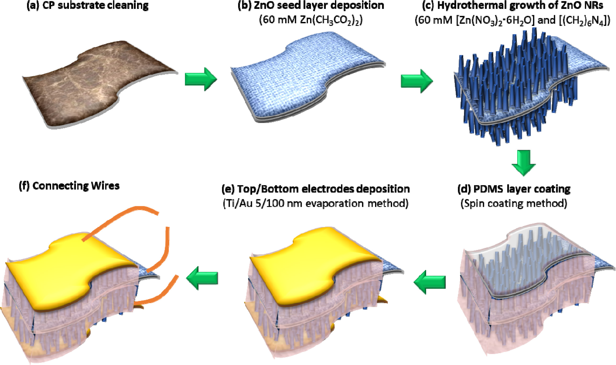
Fabrication
Fig. 1 shows the procedures for fabricating the PENG
devices from the ZnO NRs. The ZnO NRs were grown on both surfaces of the 35 μm-thick
CP substrate with a resistivity of about 10 Ω/cm2. To grow the ZnO
NRs on a single side of the CP substrate, the other side of the substrate was
covered by kapton tape during the growth. For ease of description, one of the
CP surfaces is defined as the front side (FS) and the other as the back side
(BS). To remove all contamination, each CP substrate was cleaned with acetone,
methanol, and deionized (DI) water in an ultrasonic bath for 10 min, and dried
with a mild N2 gas flow. The 0.5 cm2 area of the right
side of CP was then covered with kapton tape to prevent the growth of NRs. The
seed layer of ZnO NRs and the main layer were sequentially coated on the CP
substrate via a two-step hydrothermal process. In the first step, an ethanol
solution with 60 mM of zinc acetate [Zn(CH3CO2)2]
was stirred at 350 rpm and heated to 100 oC and held for 10
min. The process was repeated three times to ensure uniform and complete
coating of the ZnO seed layers on both sides of the porous CP surface.
In the second step, the seed layer-coated CP substrate was
used to grow ZnO NRs by a hydrothermal process using a mixed
solution of 60 mM zinc nitrate hexahydrate [Zn(NO3)2 6H2O]
and 60 mM hexamethylenetetramine [(CH2)6N4] in
DI water with stirring at 2,000 rpm and heating at 90 oC for 2
hr [15]. During the hydrothermal growth, the CP substrates were kept
vertically on a sample holder in the solution, to ensure
the same environment for both sides of the CP substrate. Then the samples were
cleaned in DI water to completely remove free-standing ZnO crystallites from
the samples by using an ultrasonic bath for 5 min. After the growth of the ZnO NRs, a 15-μm-thick
polydimethylsiloxane (PDMS; Sylgard-184, Dow
Corning, Midland, MI) layer was spin-coated on the ZnO NR surfaces. This PDMS
prepolymer was prepared with a weight ratio of 10:1 by mixing a PDMS curing
agent and a PDMS base monomer, which was coated on the ZnO NR surface by using
a spin coating rotation method at 3,000 rpm for 40 sec, followed by curing at
70 oC for 30 min. These processes were repeated for both sides
of the CP substrates. During this step, the possible presence of gas bubbles in
the top layer can hinder the connections between ZnO NRs and PDMS layers.
Therefore, the sample was evacuated in a vacuum chamber to remove the unwanted
gas bubbles from the thick PDMS layers and to strengthen the penetration of the
PDMS layer into both sides of the CP substrate. Ti/Au layers (5/100 nm) were
deposited on both sides of the PDMS-covered ZnO NRs at room temperature (RT) by
using a thermal evaporator. Finally, for observing the electrical output, Cu
wires were connected to the double-sided electrodes, as shown in Fig. 1(f).
Characterization
The surface topography and composition
of the ZnO NRs on
both sides of the CP were observed by using field-emission scanning electron microscopy (FE-SEM) and the structural properties were investigated by X-ray diffraction (XRD). The photoluminescence (PL) spectra of the ZnO NRs on both sides of the CP substrate were measured by using a
continuous wave of He-Cd laser with 24 mW power and 325 nm wavelength at RT.
The PENG devices
were subjected to an external mechanical force by a
straining system comprised of a 0.8-cm-diameter cylinder, in which the device
surface was hit repeatedly and
a periodic mechanical compressive stress was applied. In this continuous stress-and-relax process, the output
voltages were measured
simultaneously by using an
oscilloscope (TBS1202B, Tektronix).
|
Fig. 1 Schematic of the processing steps for fabricating ZnO NR-based PENGs on DSCP. |
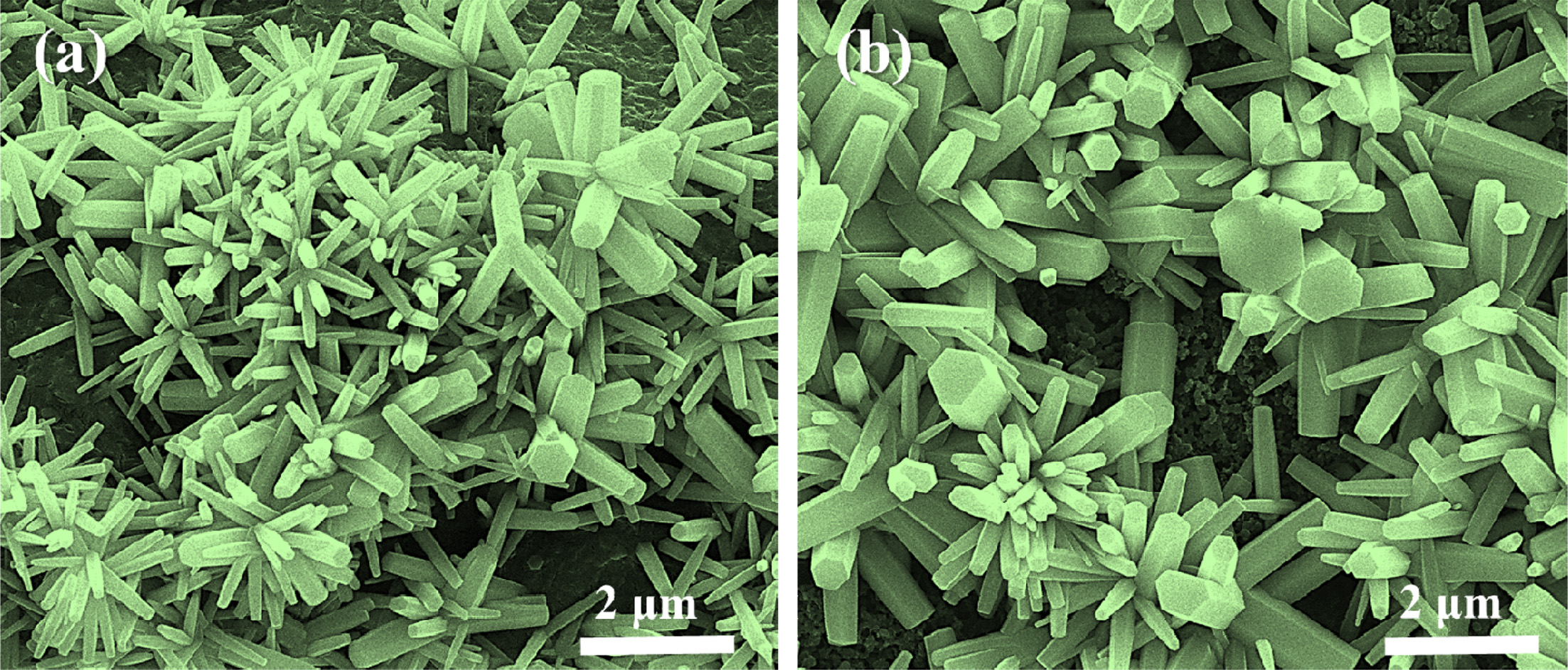
Fig. 2 shows FE-SEM images of the ZnO NRs deposited on the
front and back of CP with a molar concentration of 75 mM. The ZnO NRs on the
porous surface of CP were grown in random directions and showed a similar shape
on both sides. However, the density of the ZnO NRs was slightly higher on the
back of CP compared to that on the front. The surface of the ZnO
NRs showed a hexagonal columnar structure. This
implies that each ZnO NR was a wurtzite-structured single
crystal that was grown along the c-direction.
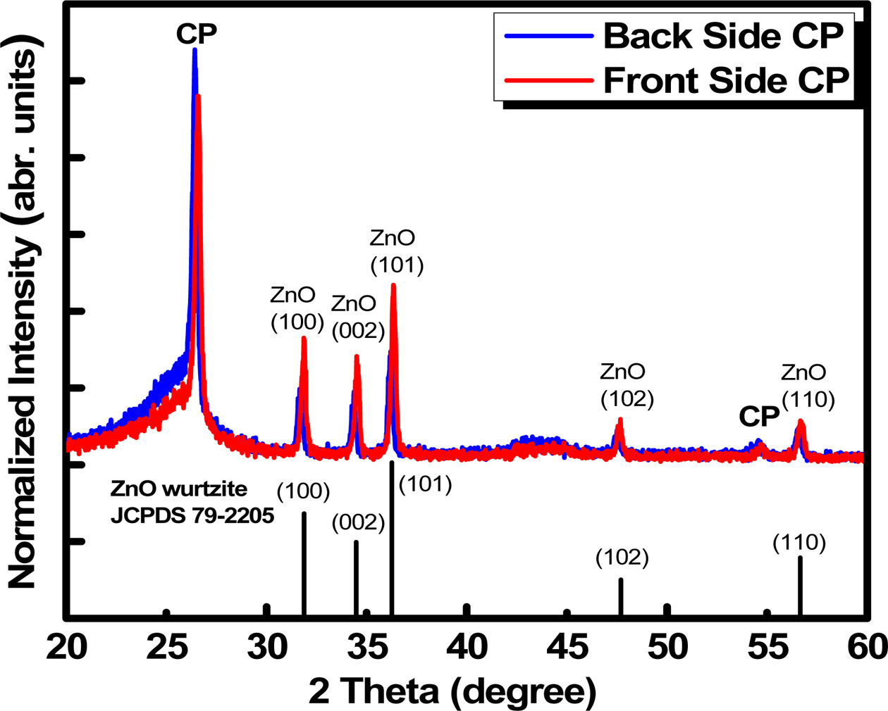
Fig. 3 shows the XRD results that reveal the crystal
structure of the ZnO NRs on both sides of the CP substrate. The broad peak at
around 26.5o is attributed to the short-range order of the amorphous
phase of the CP substrate. The sharp diffraction peaks correspond to the (100), (002),
(101), (102), and (110) planes of hexagonal wurtzite structure of ZnO (space
group: P63mc; a = 0.32501 nm, c = 0.52071 nm). The
diffraction data were in agreement with the JCPDS card for ZnO (JCPDS 79-2205). There were no diffraction peaks except those for the CP substrate and ZnO. This indicates that no secondary
phase or impurity was detected. The
substrate peaks of the ZnO NRs on the FS of the CP have greater intensity than
those of the BS, which confirms the better crystallinity of the NRs in the BS.
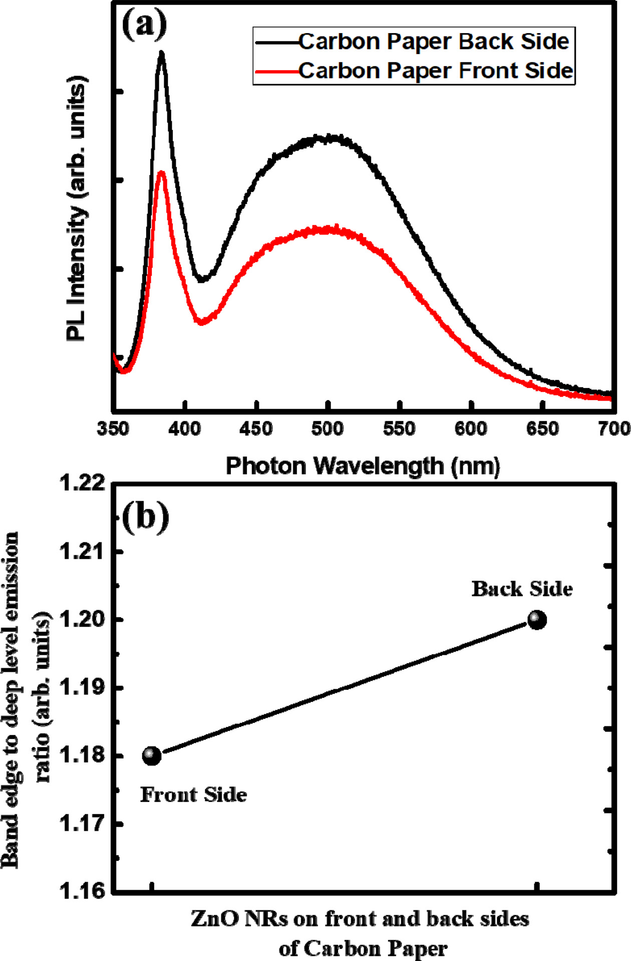
Fig. 4(a) shows the PL spectra of the ZnO NRs grown on
both sides of the porous CP substrate at RT. A sharp peak at 380 nm and a
relatively weak peak at 520 nm were observed in both FS and BS spectra. The
sharp peak in the ultraviolet range corresponds to the band-edge emission of
ZnO NRs. The broad emission band in the visible spectral range is due to the
deep level emissions from the ZnO NRs, which originate from various impurities
in the ZnO crystal, such as oxygen deficiency due to electron recombination,
zinc interstitials, and their complexes [22, 23]. These point defects usually
act as a donor to generate free charge carriers. The generated free charge
carriers in the ZnO NRs are detrimentally affected by screening the
generated piezoelectric potential on the output
voltage performance of the designed PENG devices [7, 24, 25].
Therefore, the crystalline quality of the ZnO NRs on each side of the CP
substrate was investigated by comparing the intensity of the deep level
emission. Fig. 4(b) shows the PL peak intensity ratio of the band-edge to the
deep level emissions from the ZnO NRs on both sides of the CP substrate. The
intensity ratios of 1.18 and 1.20 on the FS and BS, respectively, imply that
the ZnO NRs’ crystalline quality was slightly better on the BS than on the
FS. This result agrees with the morphological results that show
the vividly uniform and denser growth of ZnO NRs on the back as shown in Fig.
2(b). This is attributed to the inevitable difference in the amounts of Zn and
O supplied to both sides of the substrate during the hydrothermal growth.
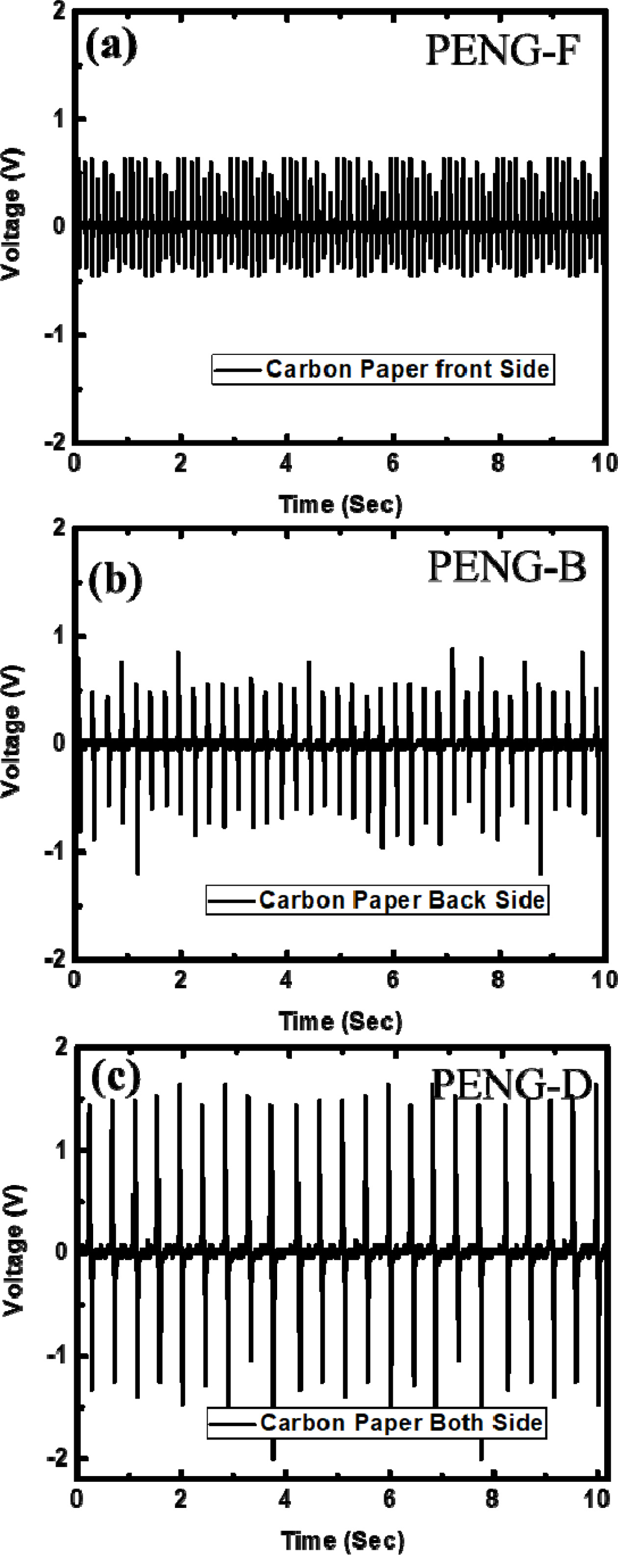
Fig. 5 shows the voltage outputs of the PENG devices
fabricated on the DSCP substrate with the same strain frequency at
2.2 Hz. For simplicity, we denoted PENGs on the front
only, back only, and double sided as PENG-F, PENG-B, and PENG-D, respectively.
When stress is applied to and released from the PENGs, despite the variation in
output voltage on each side, all three PENGs showed positive and negative peaks
due to the charging and discharging, respectively. This is attributed
to the alternating current (AC) signals produced by the
stress along the perpendicular direction to the vertically aligned ZnO NRs in
the PENG device. The figure shows that the output voltage remains an AC signal while the ZnO NRs
are grown in random direction, which is
attributed to the elastomeric property
of the PDMS polymer layer which helps the transfer of the applied strain to
both the whole PENG device and the individual ZnO NRs. The Young’s modulus of
the PDMS polymer ranges between 0.57 and 3.7 MPa [26], while that of the ZnO
NRs is about 29 GPa [27]. Therefore, the Young’s modulus is about four orders
of magnitude larger for the ZnO NRs than that for the PDMS layer. As a result,
when the stress is applied to the PENG device, the PDMS layer is deformed first
and the stress is distributed to the individual ZnO NRs equally [28]. Therefore, the PDMS layer plays a
critical role in transferring the
applied stress in this PENG device in the isotropic directions to the ZnO NRs.
PENG-B generated a larger output voltage (0.88V) than
PENG-F (0.64 V) due to the denser ZnO NRs, as shown in Fig. 2, and exhibited
better crystallinity, as shown in Fig. 3. The free charge carriers that were
generated by impurities in the ZnO NRs detrimentally affected the PENG
performance by screening the generated piezoelectric potential [8, 29]. The
voltage output of PENG-D (1.64 V) was enhanced about 2.56 and 1.86-fold
compared to that of PENG-F and PENG-B, respectively. The enhanced voltage
output would attributed to the electric field-induced synergetic effect between
the front and back of the CP substrate and the modification of the CP substrate
resistance under the electric field generated by the PENGs. And this enhancement mechanism can be explained as follows.
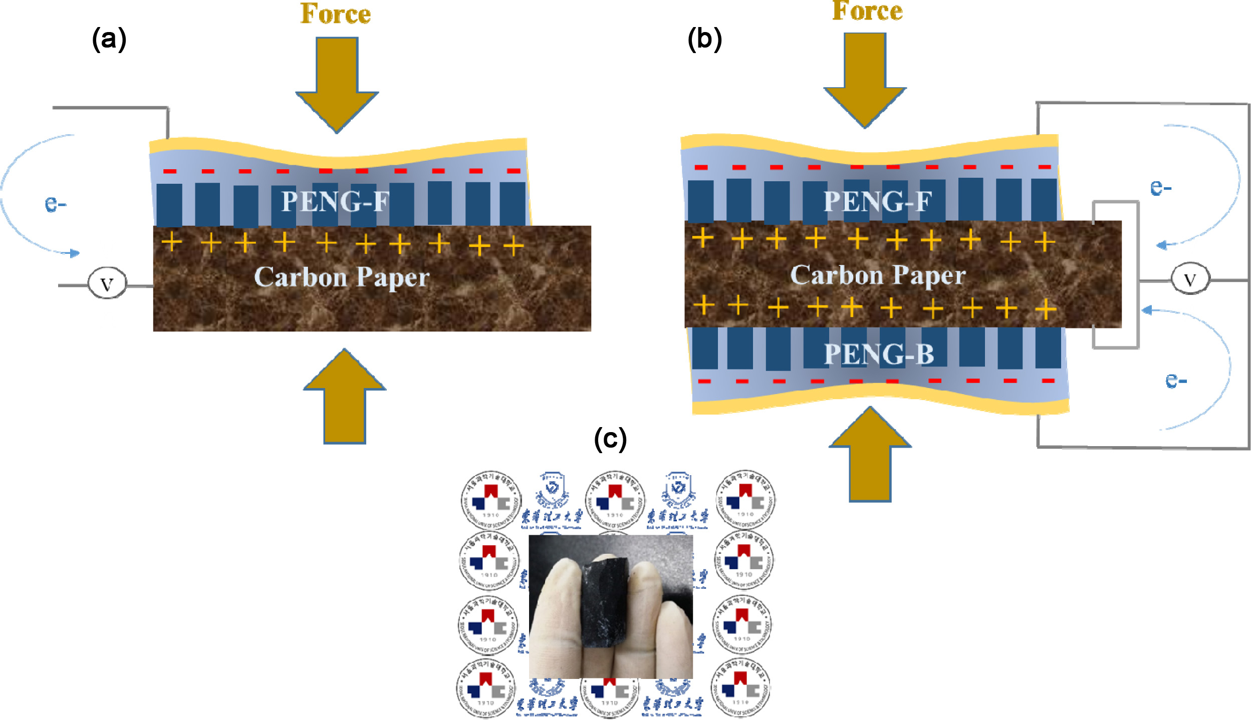
Fig. 6 shows the operating principle and enhancement mechanism of the PENG
device on the CP substrates. A negative potential is initially created at the
top of the ZnO NRs when stress is applied to only one side of the PENG device,
and is then delivered to the electrodes through the PDMS layers, thus
generating a negative pulse. As the stress is subsequently removed, the
piezoelectric potential suddenly vanishes, which allows the stored charge in
the electrode to return through the external circuit and generate a positive
pulse, as occurs in other ZnO NR-based PENG devices. The operation principle of
PENG-D can be regarded as a combination of two devices. The piezoelectric potential generated as the ZnO NR experiences an external tensile or com- pression
stress on the surface causes relative displacement of Zn2+ cations with respect to O2-
anions. The amount of maximum piezoelectric potential generated from a single ZnO NR under external mechanical stress for
vertical (FV) and lateral (FL)
directions can be expressed as Vmax = |FV|gV(L/pR2)
and Vmax = |FL|gL(1/pR),
respectively [7,10,28], where gV
and γL denote the piezoelectric voltage parameters in
vertical and lateral directions of ZnO NRs, respectively, and R and L
denote the radius and length of each ZnO NR, respectively. These equations
imply that if the NR’s radius and length are unchanged then the piezoelectric
output from each ZnO NR is always constant and is directly proportional to the
maximum deflection of the individual NR. Therefore, as the number of ZnO NRs in
the PENG devices increases, greater piezoelectric potential is generated
because each ZnO NR can act as an individual voltage source. This is consistent
with the results that the output voltages from PENG-D are enhanced by 2.56 and
1.86-fold compared to that of PENG-F and PENG-B, respectively. In PENG-D, the
electrons of both sides sequentially enforce and then reinforce the flow from
the PENG device where the electric field is generated. This enables more
electrons to flow through the external circuit and accumulate together
and finally be measured by using the connected measurement
systems. An electric field-induced synergetic effect
between PENG-F and PENG-B enhanced the PENG-D output, which was 1.08-fold
greater than the sum of the individual voltage outputs of PENG-F and PENG-B.
This explains the enhanced output voltage performance from PENG-D compared to
that of the two single-sided PENG devices. This enhancement is further
attributed to the modification of the electrical properties under a generated
electric field. Due to the electron scattering mechanism, the resistance of the
substrate can be modified under an electric field [30]. Therefore, PENG-D can
enhance the output voltage. In addition, the flexibility of the fabricated
device, as shown in Fig. 6(c), will allow its use in bendable applications such
as for in-vitro medical sensors and textile devices.
|
Fig. 2 FE-SEM images of the ZnO NRs on DSCP: (a) FS and (b) BS. |
|
Fig. 3 XRD patterns of ZnO NRs on DSCP. |
|
Fig. 4 (a) Comparison of PL spectra for the front and back of
carbon paper measured at RT for ZnO NRs on DSCP. (b) The
band-edge emission to deep level emission ratio for the ZnO NRs
grown on the front and back of DSCP. |
|
Fig. 5 Output voltage from ZnO NRs-based PENGs on carbon
paper: (a) PENG-F, (b) PENG-B, and (c) PENG-D under a strain
frequency of 2.2 Hz. |
|
Fig. 6 Schematic of PENG device structure on (a) single side (either front or back) and (b) DSCP substrates operating under compressive
stress. (c) Bendability of the PENG device on DSCP. |
In summary, we have fabricated ZnO NR-based PENGs
exhibiting enhanced output voltage by using a DSCP substrate. Morphological
investigation showed that the ZnO NRs were grown in the similar shape and
length on both sides of the CP surface, but with a slightly larger density on
the back. The XRD and PL results confirmed that the crystal quality of the ZnO
NRs on both sides of the substrate exhibited similar degree. The voltage output
from PENG-D was 2.56- and 1.86-fold greater than those from PENG-F and PENG-B,
respectively. The enhanced voltage output is attributed to the electric
field-induced synergetic effect between the front and back of the CP substrate
and the modified electrical resistance of the CP substrate under the electric
field generated by the operating PENGs. These results demonstrate the
capability of the ZnO NR-based PENG on the DSCP to enhance their output voltage
as well as the possible application to bendable self-powering devices.
This study was supported by the Research program funded by
the Seoultech (Seoul National University of Science & Technology)
- 1. Z.L. Wang and J. Song, Science 312 (2006) 242-246.
-

- 2. Z.L. Wang, Sci. Am. 298 (2008) 82-87.
-
- 3. Y. Hu, Y. Zhang, C. Xu, L. Lin, R.L. Snyder, and Z.L. Wang, Nano Lett. 11 (2011) 2572-2577.
-
- 4. Z.L. Wang and W. Wu, Angew. Chem. Int. Ed. 51 (2012) 11700-11721.
-
- 5. K.K. Kim and I.K. Park, J. Ceram. Process. Res. 18 (2017) 435-439.
- 6. S. Beeby, M. Tudor, and N. White, Meas. Sci. Technol. (2006) R175.
-
- 7. J. Sohn, S. Cha, B. Song, S. Lee, S. Kim, J. Ku, H. Kim, Y. Park, B. Choi, Z L. Wang, J.M. Kim, and K. Kim, Energy Environ. Sci. (2013) 97-104.
-
- 8. M.Y. Choi, D. Choi, M.J. Jin, I. Kim, S.H. Kim, J.Y. Choi, S.Y. Lee, J.M. Kim, and S.W. Kim, Adv. Mater. 21 (2009) 2185-2189.
-
- 9. H.K. Park, K.Y. Lee, J.S. Seo, J.A. Jeong, H.K. Kim, D. Choi, and S.W. Kim, Adv. Funct. Mater. 21 (2011) 1187-1193.
-
- 10. Y. Gao and Z.L. Wang, Nano Lett. 7 (2007) 2499-2505.
-
- 11. D.Y. Lee, H. Kim, H.M. Li, A.R. Jang, Y.D. Lim, S.N. Cha, Y.J. Park, D.J. Kang, and W.J. Yoo, Nanotechnology 24 (2013).
-
- 12. D.Y. Jung, S.H. Baek, M.R. Hasan, and I.K. Park, J. Alloy Compd. 641 (2015) 163-169.
-
- 13. G.H. Nam, S.H. Baek, C.H. Cho, and I.K. Park, Nanoscale 6 (2014) 11653-11658.
-
- 14. M.R. Hasan, S.H. Baek, K.S. Seong, J.H. Kim, and I.K. Park, ACS Appl. Mater. Inter. 7 (2015) 5768-5774.
-
- 15. G.M.H.U. Banna and I.K. Park, Nanotechnology 28 (2017) 445402.
-
- 16. S.H. Baek, M.R. Hasan, and I.K. Park, Nanotechnology 27 (2016) 065401.
-
- 17. C. Xu and Z.L. Wang, Adv. Mater. 23 (2011) 873-877.
-
- 18. C. Liu, A. Yu, M. Peng, M. Song, W. Liu, Y. Zhang, and J. Zhai, J. Phys. Chem. C 120 (2016) 6971-6977.
-
- 19. K. Y. Lee, J. Chun, J.H. Lee, K.N. Kim, N.R. Kang, J.Y. Kim, M.H. Kim, K.S. Shin, M.K. Gupta, J.M. Baik, and S.W. Kim, Adv. Mater. 26 (2014) 5037-5042.
-
- 20. K.I. Park, C.K. Jeong, J. Ryu, G.T. Hwang, and K.J. Lee, Adv. Energy Mater. 3 (2013) 1539-1544.
-
- 21. G. Zhu, R. Yang, S. Wang, and Z.L. Wang, Nano Lett. 10 (2010) 3151-3155.
-
- 22. L.E. Greene, M. Law, J. Goldberger, F. Kim, J.C. Johnson, Y. Zhang, R.J. Saykally, and P. Yang, Angew. Chem. Int. Ed. 42 (2003) 3031-3034.
-
- 23. A.C. Arsenault, T.J. Clark, G. Von Freymann, L. Cademartiri, R. Sapienza, J. Bertolotti, E. Vekris, S. Wong, V. Kitaev, I. Manners, R. Z. Wang, S. John, D. Wiersma, and G.A. Ozin, Nat. Mater. 5 (2006) 179-184.
-
- 24. D. Li, Y.H. Leung, A.B. Djurišić, Z.T. Liu, M.H. Xie, S.L. Shi, S.J. Xu, and W.K. Chan, Appl. Phys. Lett. 85 (2004) 1601-1603.
-
- 25. R. Yang, Y. Qin, L. Dai, and Z.L. Wang, Nat. Nanotech. 4 (2009) 34-39.
-
- 26. J. Song, X. Wang, E. Riedo, and Z.L. Wang, Nano Lett. 5 (2005) 1954-1958.
-
- 27. X. Li, Y. Chen, A. Kumar, A. Mahmoud, J.A. Nychka, and H.J. Chung, ACS Appl. Mater. Inter. 7 (2015) 20753-20760.
-
- 28. G. Romano, G. Mantini, A. Di Carlo, A. D’Amico, C. Falconi, and Z.L. Wang, Nanotechnology 22 (2011) 465401.
-
- 29. D. Kim, K.Y. Lee, M.K. Gupta, S. Majumder, and S.W. Kim, Adv. Funct. Mater. 24 (2014) 6949-6955.
-
- 30. E. Ahilea and A.A. Hirsch, J. Appl. Phys. 42 (1971) 5601-5608.
-
 This Article
-
2020; 21(6): 656-661
Published on Dec 31, 2020
- 10.36410/jcpr.2020.21.6.656
- Received on May 20, 2020
- Revised on Jul 2, 2020
- Accepted on Jul 16, 2020
Services
- Abstract
introduction
experimental procedure
results and discussion
conclusions
- Acknowledgements
- References
- Full Text PDF
Shared
Correspondence to
- Il-Kyu Park
-
Department of Materials Science and Engineering, Seoul National University of Science and Technology, Seoul 01811, South Korea
Tel : +82-2-970-6349 Fax: +82-2-973-6657 - E-mail: pik@seoultech.ac.kr
Clean-Energy Research Institute(CRI), Hanyang University, 222, Wangsimni-ro, Seongdong-gu, Seoul, 04763, Korea
E-mail: jcpr@hanyang.ac.kr