


- Effect of annealing temperature on the optical properties of a bulk GaN substrate
Hee Ae Leea, Joo Hyung Leea, Seung Hoon Leea, Hyo Sang Kangb, Seong Kuk Leeb, Nuri Oha, Won Il Parka and Jae Hwa Parkb,*
aDivision of Materials Science and Engineering, Hanyang University, Seoul 04763, Republic of Korea
bAMES Micron Co. LTD, 32 Singok-ro, Gochon-eup, Gimpo-si, Gyeonggi-do, 10126, Republic of Korea
Variation of optical
properties in a bulk GaN substrate have experimentally investigated with
respect to different annealing conditions of 700 - 1,000 oC.
As-annealed GaN was characterized by scanning electron microscopy,
photoluminescence, and Raman spectroscopy. The experimental results
demonstrated that the crystallinity and internal residual compressive stress of
GaN are most effectively improved when heat-treated at 900 oC for
three hours. The optical characteristics were also improved by enhancing the
quality of the GaN substrate by decreasing both the defect density and the
residual stress. It was also confirmed that the effect of the heat treatment
was excellent given that impurities were effectively removed by this process.
Keywords: Hydride vapor phase epitaxy, Gallium nitride, Optical property, Crystallinity, Residual stress, Defect density
GaN is a III-V compound semiconductor with a wide band
gap. Therefore, it is a material that is expected to be applied to
light-emitting devices operating in the blue or ultraviolet range [1, 2]. It
has a number of excellent properties, such as very good luminescence,
structural stability at high temperatures, high hardness, high thermal
conduction, and good chemical stability. Therefore, it
can be used in a wide variety of applications, not only in
optical devices but also in high-power and high-temperatures
devices. Based on these characteristics, numerous
studies have sought to apply GaN to high-brightness light-emitting diodes (LED)
and laser diodes (LD). Recently, it is also the subject of increasing
interest regarding its application to power and communication
semiconductors such as those that power RF and other devices [3-7].
The characteristics of the substrate are very important
when attempting to produce a GaN device capable of high brightness and high
performance. The GaN single crystal difficult the growth for ingot single
crystal which can get the substrate of high quality. Because ingot growth
requires a pressure above 6 GPa and a temperature above 2,200 oC due
to the properties of nitrogen [8]. Therefore, the growth of GaN depends on epitaxial
growth, mainly using a heterogeneous substrate. Heterogeneous
substrates mainly utilize sapphire substrates for economic
reasons [9-11]. Sapphire impedes the acquisition of a high-quality GaN
epi-layer due to its large lattice mismatch and difference in the thermal
expansion coefficient from that of GaN. Hence, the interior of GaN single
crystal grown on sapphire has a high density (typically in the range of 108~109
cm-2)
of threading dislocations and residual stress [12-14].
These dislocations and defects
play a role in reducing the lifetime and efficiency of these devices by
creating, for example, a center of non-radiation recombinations or charge
leakage paths [15, 16]. The residual stress changes the crystalline symmetry
and exerts an effect the basic physical properties of the materials and the
structure of the electronic band [17]. When the residual stress inside the GaN single
crystal increases, it generates or propagates cracks to mitigate the stress resulting
in new defects. These act the factors that deteriorate the quality of the GaN
substrate, including optical and electronic properties [18-20]. In addition, a
damage layer is formed under the surface of GaN during
mechanical polishing, a step during the substrate manufacturing process, resulting in deterioration of the optical and
electrical properties of the device [21, 22]. For use in high-quality
electronic and optical devices, there is a need for a method capable of
mitigating these problems and
improving the properties of GaN. Annealing is known to be a feasible
method for improving the elec- tronic and optical properties of nitride
semiconductors [3, 23]. However, most
of the annealing studies involving
GaN focused on dopant implantation. Few studies have concentrated on the
effects of a heat treatment on the optical damage recovery of mechanically
polished bulk GaN [21, 24]. Therefore, in this work, Therefore, in this work,
we investigated variations of the optical characteristics after a heat
treatment for bulk GaN substrate grown on a sapphire substrate using the hydride vapor phase epitaxy (HVPE) technique.
Bulk single-crystal GaN was grown at a thickness of 1.0 mm
or more on a c-plane sapphire (0001) substrate using a HVPE system. GaCl gas as
a Ga source was formed by reacting metal Ga with HCl gas at 700 - 800 oC.
This gas was reacted with NH3 gas, which was used
as an N source, and single-crystal GaN was grown at a
sustained growth rate of 100 μm/h at a temperature of 1,000 - 1,100 oC.
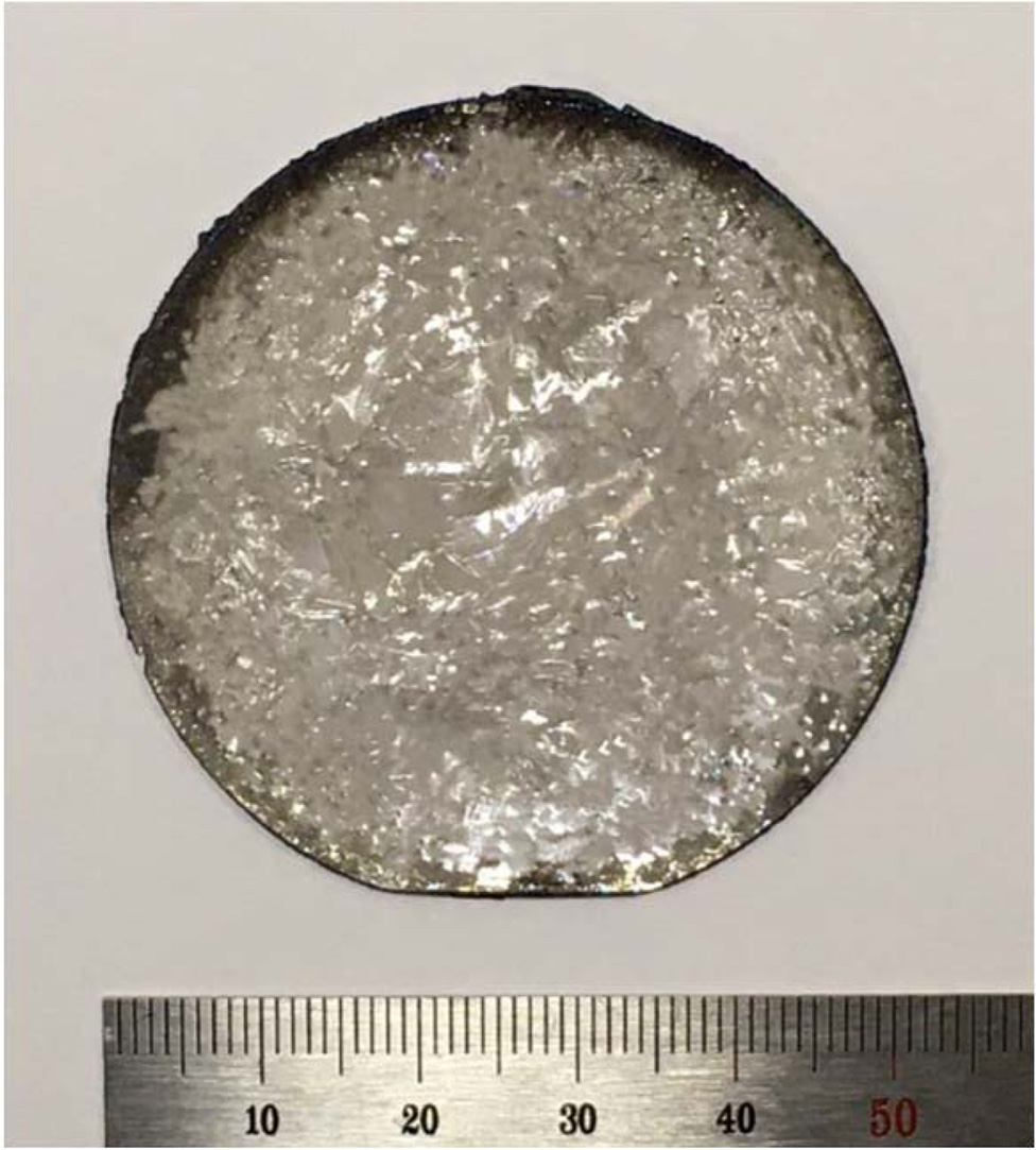
Fig. 1 shows the bulk single-crystal GaN after growth. The as-grown bulk
single-crystal GaN was separated from the sapphire substrate by a laser lift
off (LLO) process. The separated GaN was fabricated on
a two-inch GaN substrate with a thickness of 1.0 mm
after polishing. The GaN substrate was then cut into pieces 10X10 mm2 in size.
The GaN specimens were annealed in the temperature
range of 700 - 1,000 oC for one to five hours using an
independently fabricated annealing furnace. N2 ambient was used to
prevent the disassociation of nitrogen at the high temperatures used. We
analyzed the defect density of the GaN single crystal according to the heat
treatment condition after chemical etching using a melt with a KOH/NaOH
eutectic composition [25]. We confirmed etch pits on the surface of the
as-etched GaN via scanning electron microscopy (SEM, JSM-5900LV, JEOL, Japan)
when analyzing the dislocation density. Raman spectroscopy (JASCO, NRS-3100,
England) was used to characterize the residual stress, with the excitation
laser source and power level set to 532 nm and 1.3 mW,
respectively. The optical properties were analyzed by a
photoluminescence analysis (PL, Dongwoo Optron, MonoRa750i, Korea) at room temperature. During this process, the excitation
source used was a 325 nm He-Cd laser, of which the energy exceeds that of the
band gap energy of GaN. The power of the laser was set to 2.5 mW.
|
Fig. 1 Image of a 2-inch bulk GaN grown by HVPE. |
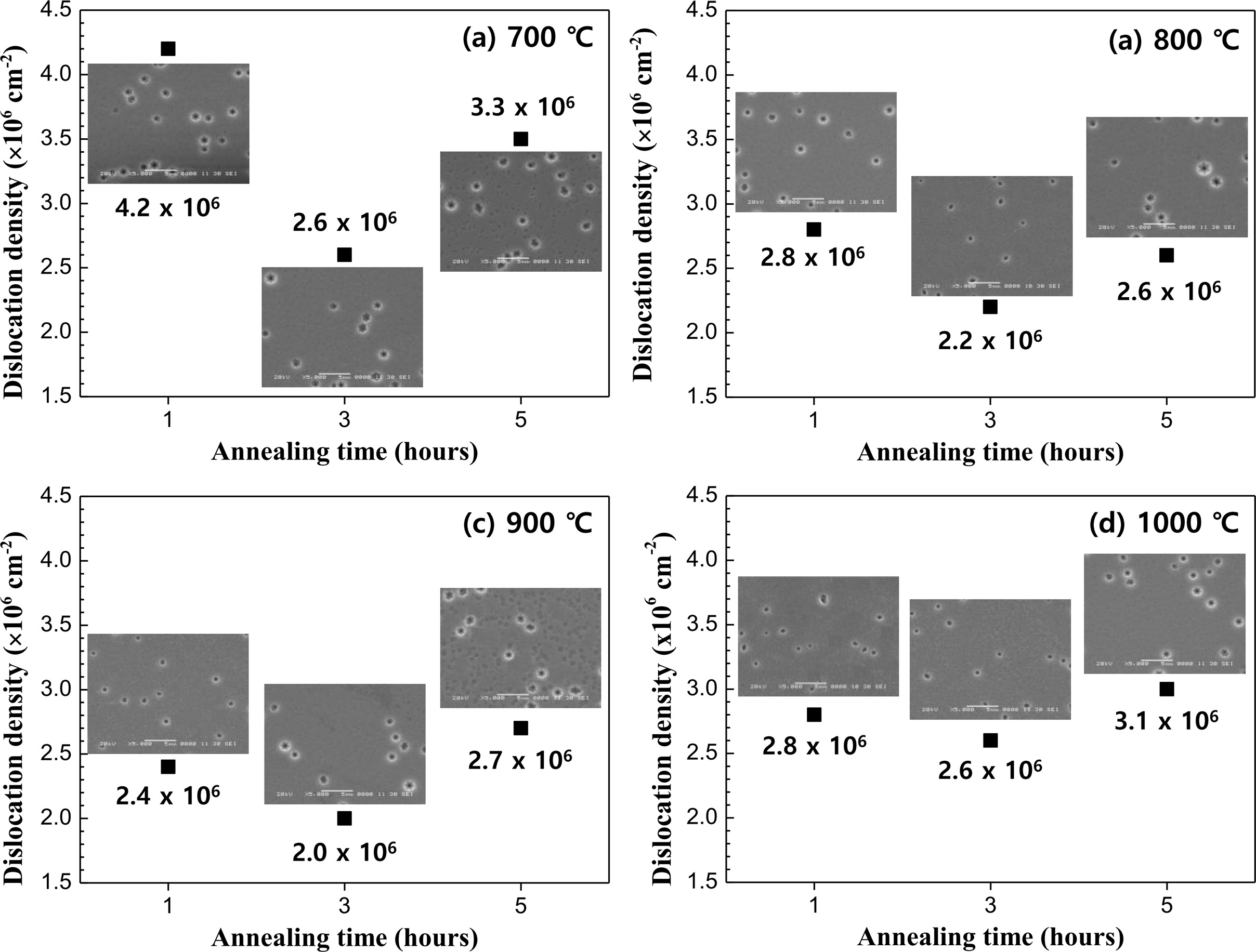
The dislocation density of the GaN substrate is a major
measure of the quality of single-crystal GaN, and a lower dislocation density
indicates good quality of the single crystal [26]. Etch pits existent in the
GaN single crystal are a type of defect deriving from
threading dislocations generated at the interface. Therefore, the
dislocation density can be obtained by calculating the density using the number
of observed etch pits [27]. For the measurement a value of etch pit density
(EPD) is calculated from the number of etch pits N within the measuring field
according to equation (1):
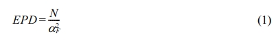
Here, aF
is the measuring field. The value of aF
must be given in cm to obtain the local EPD in cm-2
[28]. Fig. 2 presents the results after measuring the variation of the etch pit
density using an etchant with a KOH/NaOH eutectic composition after the heat
treatment. The dislocation density decreased and then increased again with an
increase in the annealing time at all temperatures after annealing. In other
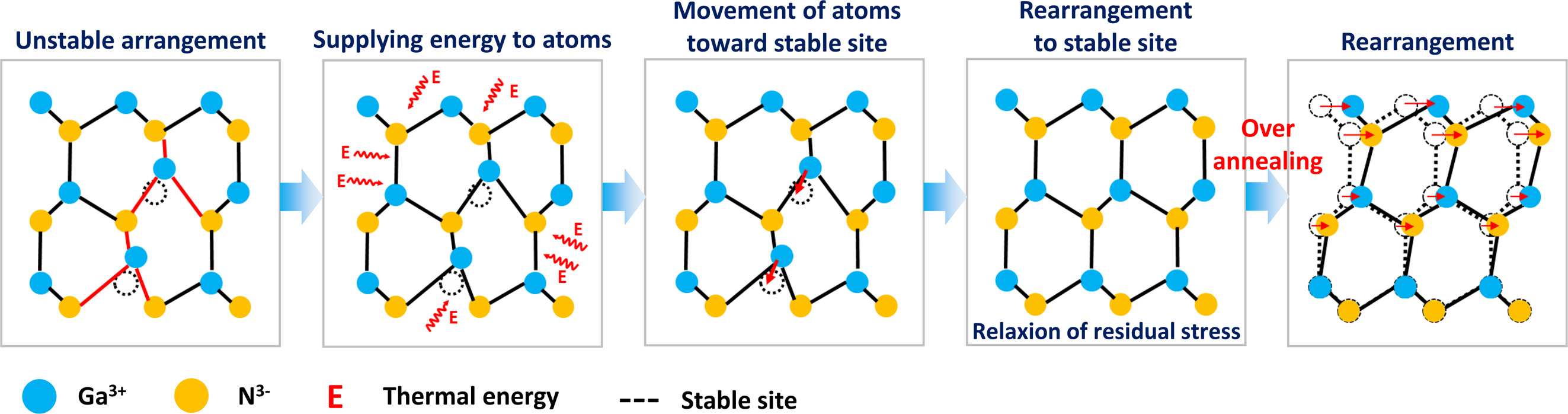
words, it was observed the same trend which the crystallinity increasing and
then decreasing. As shown in Fig. 3, an unstable lattice with high energy in
the material move in a direction such that the internal energy is reduced when
receiving energy above a critical level thermal energy by
annealing. As such, the crystallinity improves as atoms
move to stable sites and are rearranged [29]. This is the effect of the
annealing. However, the effect of annealing decreases due to the excessive heat
energy during the annealing process with increase in the heat treatment time.
Therefore, it was considered that the dislocation density was reduced after
annealing for five hours. The results of a dislocation density analysis via EPD
showed that the lowest dislocation density arose after the
sample was annealed for three hours throughout the heat
treatment temperature range, meaning that the crystallinity is most effectively
improved during the heat treatment at that time.
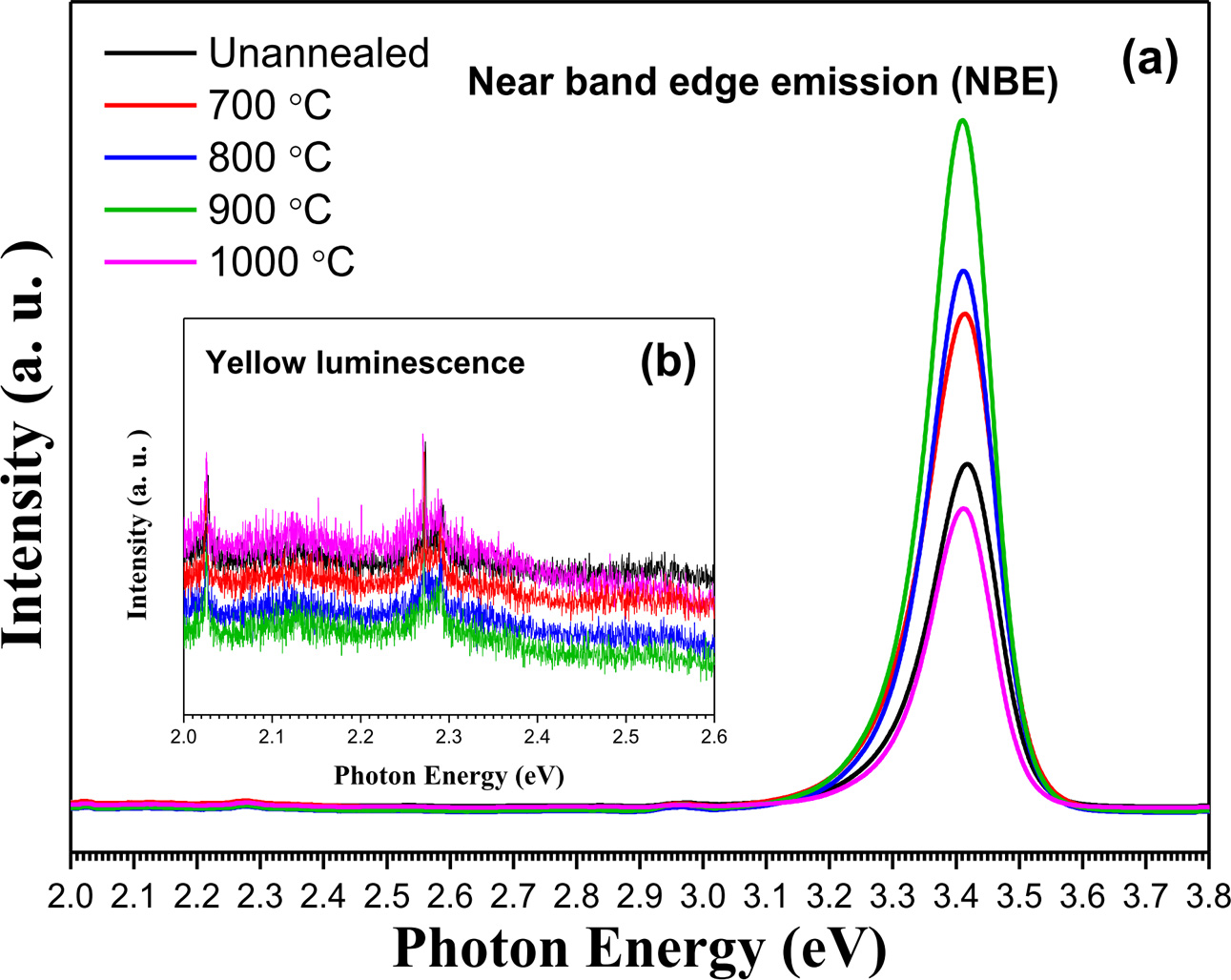
Fig. 4 shows the PL spectra measured at room temperature
for specimens annealed for three hours, at which the effects of the heat
treatment were best in all temperature ranges. The strong peak around 3.4 eV in
the PL spectra of all samples is nearly identical to that of about 3.41 eV,
which is the band gap energy of GaN. This indicates with regard to near-band
edge emission (NBE) which the luminescence caused by the death of excitons
around the energy gap. The intensity of the NBE peak increased with an increase
in the annealing temperature in the PL spectrum, meaning that the quality of
the substrate was improved [30]. However, the intensity of the peak decreased
again at 1,000 oC because the improved crystal quality was
reduced via nitrogen dissociation at a high temperature. The nitrogen can
dissociate at high temperatures of 1,000 oC or more below 4.5
GaP [31]. In other words, the nitrogen-vacancy was created due to the thermal
decomposition in high temperature and acted as a non-radiative recombination
center, resulting in a decrease in the intensity of the NBE peak. These trends
match the result of the dislocation density via measurement for EPD.
Fig. 5(a) shows a blue shift that indicates that the NBE
peak shifts toward a lower energy level with an increase in the annealing
temperature. A blue shift in the PL spectrum can appear when the interatomic
distance of the material increases, as shown in Fig. 5(c). This is believed to
stem from the fact that the interatomic distance was widened because it relaxed
the residual compressive stress generated by the difference in the thermal
expansion coefficient at the interface between the sapphire and the GaN later via
the heat treatment. To confirm this change precisely, we indicate numerically
the variation of the position of the NBE peak in Fig. 5(b). The position of the
NBE peak decreased with an increase in the annealing temperature,
showing its lowest value at the temperature of 900 oC.
Therefore, it was considered that annealing at the corresponding temperature
most effectively relaxed the residual
compressive stress.
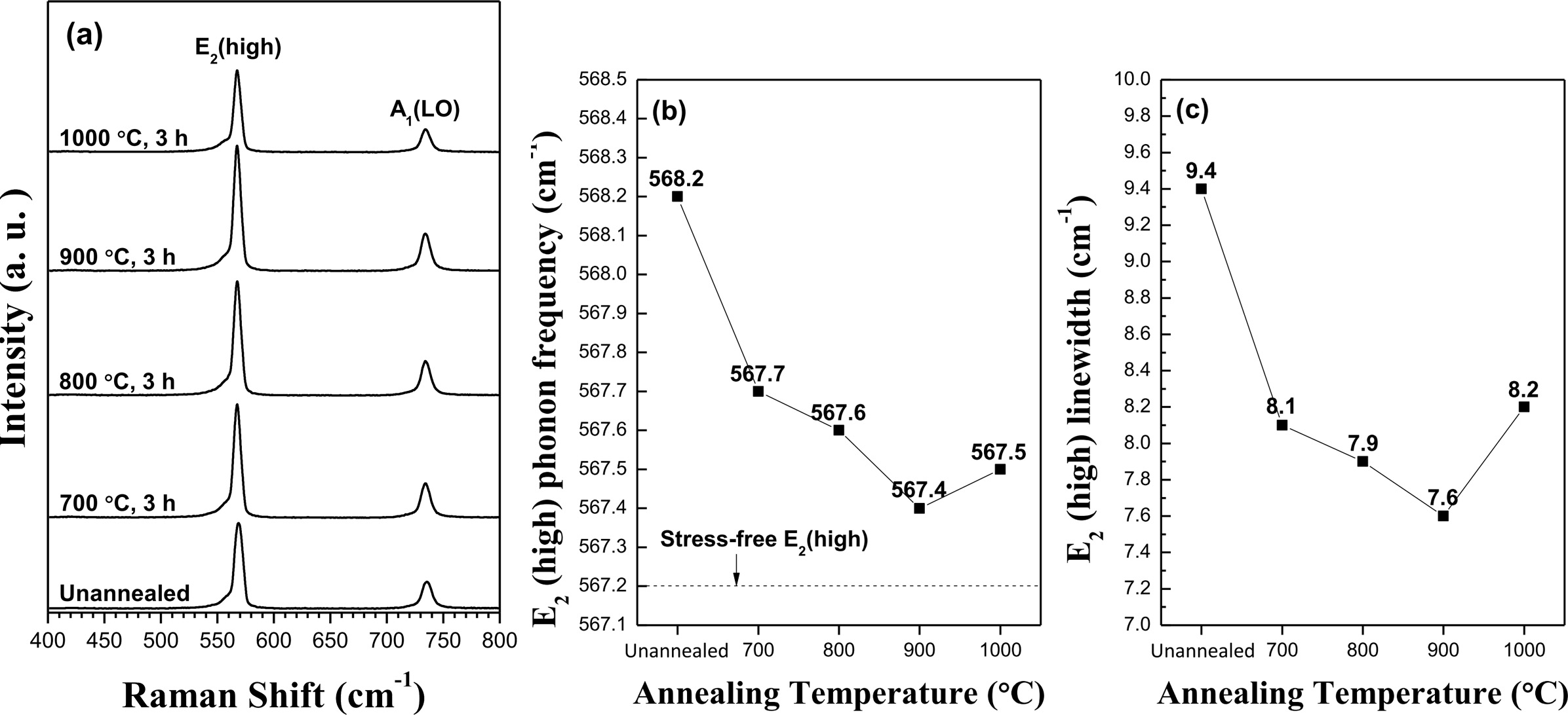
To characterize the residual stress existent in the
internal material after annealing, we undertook Raman measurements, as
indicated in Fig. 6(a). The Raman frequency modes of GaN, having
a hexagonal symmetric structure (C6v), are 2A1,
2E1, 2E2, and 2B1. For bulk GaN, six phonon
frequency modes exist: A1(TO) = 531.8
cm-1,
E1(TO) = 558.8 cm-1,
E2(low) = 144 cm-1,
E2(high) = 567.2 cm-1,
A1(LO) = 734 cm-1,
and E1(LO) = 741 cm-1.
The E2(high) mode of GaN is the mode that most sensitively reacts to
stress present inside the crystal or to external pressure. It has been reported
that the tensile stress arises during the move to a low phonon frequency and
that compressive stress arises when moving to a high phonon frequency based on
the E2(high) mode value of a stress-free crystal (about 567.2 cm-1)
[32]. For example, in the presence of tensile stress, the atomic spacing will increase
with an expansion of the lattice, and the phonon frequency will decrease. On the other hand, in the presence of
compressive stress, the atomic spacing will decrease with a contraction of the lattice, and the phonon
frequency will increase [33]. Fig.
6(b) shows the variation of the E2(high) mode peak. The E2(high)
mode, which appears strongly in the Raman spectrum, shifted to a lower
frequency with an increase in the heat treatment temperature. We confirmed that
the E2(high) value after annealing at 900 oC was
closest to the value indicated by the dotted line in a stress–free condition
which has a value when the internal stress of bulk GaN is free. This means that
the residual compressive stress of GaN substrate was relaxed with an increase
in the annealing temperature. This matches the result showing the blue shift of the NBE peak in the previously described
PL spectrum. Also, the intensity of E2(high)
mode peak varies with crystallinity, as the phonon vibrations are
sensitive to atom compositions. Therefore, higher crystal quality revealed more distinct E2 high phonon vibration
peaks [34]. We observed that the intensity of the E2(high) mode peak
was most strongly at 900 oC in Fig. 6(a). This is considered that
due to the crystallinity improved with relaxing residual stress. Moreover, the
full width at half maximum (FWHM) of E2(high) is affected by the
quality of the crystal [35]. Defects in the crystal decrease the effective wavelength of phonons by contributing
to the scattering of phonons, and the
FWHM of the phonon peak is reduced with a decrease in the defect density [36].
Fig. 6(c) indicates the variation of the FWHM of the E2(high) mode.
The FWHM of the E2(high) mode shows a decreasing trend with an
increase in the temperature to 900 oC, past which it increased
again at 1,000 oC. This is consistent with the result of
the dislocation density described above.
Thus, we confirmed that the crystallinity was most improved at a heat treatment temperature of 900 oC.
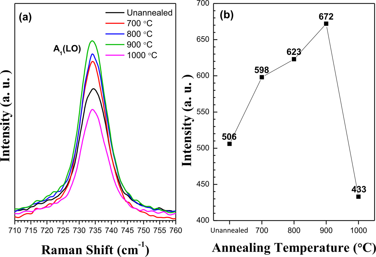
On the other hand, the yellow luminescence (YL) band at
around 2.2 eV in the PL spectrum and the A1(LO) mode at about 734 cm-1
in the Raman spectrum are peaks caused by defects and impurities. Fig. 4(b)
shows the spectrum around 2.2 eV, in which YL is generated by defects or
impurities of the crystal at a deep level. These YLs greatly degrade the
optical properties of GaN because they are related to structural defects such
as stacking defects and dislocations [37, 38]. In particular, this is a factor
that interferes with the realization of full color via the saturation of blue
emission during the manufacturing of LEDs [39]. We confirmed that the intensity
of the YL band decreased with an increase in the heat treatment temperature and
that it scarcely appeared at 900 oC. Recently, it has been reported
that nitrogen vacancies [40], C-O-related impurities [41], and Si impurities
exist in dislocations [42] and cause this YL band. However, this has not been
clearly verified.
The A1(LO) mode in the Raman spectrum changes
of its frequency according to the number of impurities contained in the
internal defects [43]. The intensity of the Al(LO) mode decreases
with an increase in the carrier concentration when the number of impurities
increases [44]. Fig. 7(a) shows the variation of the A1(LO) mode
peak before and after annealing. The intensity of the A1(LO) mode
peak increased with an increase in the heat treatment temperature. Fig. 7(b)
presents a graph that quantifies the variation of the intensity of the A1(LO)
mode peak. The intensity of the A1(LO) mode increased the most after
annealing at 900 oC. Thus, it can be determined that defects in the
crystal decreased because the number of impurities decreased after annealing
under the this conditions. However, the intensity of the peak of the A1(LO)
mode decreased after annealing at 1,000 oC. This
is considered to have occurred because the carrier concentration
was increased due to nitrogen vacancies, leading to the disassociation of
nitrogen at a high temperature. In other words, it is likely that the heat
treatment effect deteriorated as nitrogen vacancies acted as defects.
|
Fig. 2 Etch pit density of the (0002) GaN after annealing at (a) 700, (b) 800, (c) 900, and (d) 1,000 oC. |
|
Fig. 3 Schematic of behavior of atoms during heat treatment. |
|
Fig. 4 (a) the PL spectra for specimens annealed for three hours (b) the spectrum of yellow luminescence around 2.2 eV |
|
Fig. 5 (a) the shift of NBE peak in PL spectrum for bulk GaN
unannealed and annealed, (b) the variation of the position of the
NBE peak, and (c) the formation of energy bands in crystals [45,
46]. |
|
Fig. 6 (a) Raman spectra of GaN single crystal unannealed and annealed, the variation of (b) the E2 (high) and (c) the FWHM of the E2 (high)
mode. |
|
Fig. 7 (a) the spectra of A1 (LO) mode for the GaN unannealed
and annealed and (b) the variation of the intensity of the A1 (LO)
mode peak. |
We annealed a bulk GaN under various conditions. We
confirmed that the dislocation density of a bulk GaN substrate was reduced when
a heat treatment at all temperatures for three hours via an EPD analysis. Based
on this, we analyzed the optical characteristics of specimens
annealed for three hours in the temperature range of
700 - 1,000 oC. It was observed that the optical
properties of annealed bulk GaN were best after annealing at 900 oC
with an increase in the intensity of the NBE peak as the temperature was
increased up to the temperature range of 700 - 900 oC.
As a result of Raman measurements, the residual compressive stress was found to
be relaxed with an increase in the heat treatment temperature, showing a value
closest to the stress-free value at 900 oC. This
confirmed that impurities in the crystal were effectively
controlled under this condition via the variation for the YL band of the PL and
A1(LO) Raman modes. When annealing at a temperature of 1,000 oC, the effect of annealing was
found to have decreased upon an evaluation of the optical
properties and residual stress. This likely occurred due to
nitrogen vacancies which were generated given the nitrogen
dissociation that occurred at a high temperature and functioned as defects. All
things considered, the relaxation of the residual stress and the
crystallinity are superior when the heat treatment takes place at 900 oC
and lasts for three hours in the case of a bulk GaN
substrate with a thickness of 1 mm. Therefore, it could be
confirmed that the optical properties were most
effectively improved because the effect of annealing was best
under the this condition.
This work was supported by the Industrial Strategic
Technology Development program funded by the Ministry of Trade Industry &
Energy of Korea (Project No. 10080599). Raman analysis were supported by
Hanyang LINC Analytical Equipment Center (Seoul).
- 1. H. Morkoç, S. Strite, G. B. Gao, M. E. Lin, B. Sverdlov, and M. Burns, J. Appl. Phys. 76 (1994) 1363-1398.
-

- 2. S. Yoshida, S. Misawa, and S. Gonda, J. Appl. Phys. 53 (1982) 6844-6848.
-
- 3. I. Susanto, K.-Y. Kan, I.-S. Yu, J. Alloys Compd. 723 (2017) 21-29.
-
- 4. A. Bchetnia, I. Kemis, A. Touré, W. Fathallah, T. Boufaden, B. El Jani, Semicond. Sci. Technol. 23 (2008) 125025.
-
- 5. J. A Freitas Jr, J. Phys. D: Appl. Phys. 43 (2010) 073001.
-
- 6. H. Lei, H.S. Leipner, J. Schreiber, J.L. Weyher, T. Wosiʼnski, I. Grzegory, J. Appl. Phys. 92[11] (2002) 6666-6670.
-
- 7. R. Dwiliʼnski, R. Doradzinski, J. Garczynski. L. Sierzputowski, R. Kucharski, M. Zajac, M. Rudzinski, R. Kudrawiec, J. Serafinczuk, W. Strupinski, J. Cryst. Growth. 312 (2010) 2499-2502.
-
- 8. S. Krukowski, Cryst. Res. Technol. 34[5-6] (1999) 785-795.
-
- 9. C.-F Zhu, W.-K. Fong, B.-H. Leung, C.-C. Cheng, and C. Surya, IEEE Trans. Electron Devices 48[6] (2001) 1225-1230.
-
- 10. J. A Freitas Jr, J. Phys. D: Appl. Phys. 43 (2010) 073001.
-
- 11. J.H. Park, H.A. Lee, J.H. Lee, C.W. Park, J.H. Lee, H.S. Kang, H.M. Kim, S.H. Kang, S.Y. Bang, S.K. Lee, K.B. Shim, J. Ceram. Proces. Res. 18[2] (2017) 93-97.
- 12. K. Motoki, SEI Technical 70 (2010) 99-136 .
- 13. S.T. Kim, Y.J. Lee, D.C. Moon, C.H. Hong, T.K. Yoo, J. Crys. Growth 194 (1998) 37-42.
-
- 14. H. Iwata, H. Kobayashi, T. Kamiya, R. Kamei, H. Saka, N. Sawaki, M. Irie, Y. Honda, H. Amano, J. Cryst. Growth 468 (2017) 835-838.
-
- 15. M. Matys, M. Miczek, B. Adamowicz, Z.R. Zytkiewicz, E. Kaminska, A. Piotrowska, and T. Hashizume, Acta Physica Polonica A 120 (2011) A73-A75.
-
- 16. K. Motoki, SEI Technical 70 (2010) 28-35.
- 17. V. Darakchieva, T. Paskova, M. Schubert, H. Arwin, P.P. Paskov, B. Monemar, D. Hommel, M. Heuken, J. Off, F. Scholz, B. A. Haskell, P. T. Fini, J. S. Speck and S. Nakamura, Phys. Rev. B 75 (2007) 195217.
-
- 18. H. Fujikura, T. Inoue, T. Kitamura, T. Konno, T. Suzuki, T. Fujimoto, T. Yoshida, M. Shibata, T. Saito, Phys. Status Solidi B 2018 (2018) 1-11.
- 19. D. Pastor, R. Cuscó, L. Artús, G. González-Díaz, E. Iborra, J. Jiménez, F. Peiró, E. Calleja, J. Appl. Phys. 100 (2006) 043508.
-
- 20. J. Guo, H. Fu, B. Pan, R. Kang, Chin. J. Aeronaut. (2020)
- 21. J.H. Ryu, D.K. Oh, S.T. Yoon, B.G. Choi, J.W. Yoon, K.B. Shim, J. Cryst. Growth 292 (2006) 206-211.
-
- 22. D.K. Oh, S.Y. Bang, B.G. Choi, P. Maneeratanasarn, S.K. Lee, J.H. Chung, J.A. Freitas Jr, KB. Shim, J. Cryst. Growth 356 (2012) 22-25.
-
- 23. M.Y. Lee, and H.S. Im, J. Korean Phys. Soc. 60[10] (2012) 1809-1813.
-
- 24. T.W. Kang, S.U. Yuldashev, D.Y. Kim, T.W. Kim, Jpn. Appl. Phys. 39 (2000) L25-L27.
-
- 25. J.H. Park, Y.P. Hong, C.W. Park, H.M. Kim, D.K. Oh, B.G. Choi, S.K. Lee, K.B. Shim, J. Korean Cryst. Growth Cryst. Technol. 24 (2014) 135-139.
-
- 26. Y. Saighsa, in “Advanced Piezoelectric Materials” (Woodhead Publishing. 2010) p.171-203.
-
- 27. J. Chen, J.F. Wang, H. Wang, J.J. Zhu, S.M. Zhang, D.G. Zhao, D.S. Jiang, H. Yang, U. Jahn and K.H. Ploog, Semicond. Sci. Technol. 21 (2006) 1229-1235.
-
- 28. SEMI, No.M83-1112 (2014) p.10.
- 29. W.F. Smith, J. Hashemi, in “Foundation of Materials Science and Engineering, 4th edition” (SciTech Media, 2005) p.217-220.
- 30. Y. Inoue, T. Hoshino, S. Takeda, K. Ishino, A. Ishida, and H. Fujiyasu, Appl. Phys. Lett. 85 (2004) 2340-2342.
-
- 31. B.N. Feigelson, R.M. Frazier, M. Gowda, J.A. Freitas Jr, M. Fatemi, M.A. Mastro, J.G. Tischler, J. cryst. Growrh 310[17] (2008) 3934-3940.
-
- 32. G. Nootz, A. Schulte, L. Chernyak, A. Osinsky, J. Jasinski, M. Benamara, Z. Liliental-Weber, Appl. Phys. Lett. 80[8] (2002) 1355.
-
- 33. F.C. Wang, C.L. Cheng, Y.F Chen, C.C. Yang, Semicond. Sci. Technol. 22 (2017) 896-899.
-
- 34. K. Upadhyaya, S. Sharvani, N. Ayachit, and S.M. Shivaprasad, RCS Adv. 9 (2019) 28554-28560.
-
- 35. J.M.H. MSci, in “Raman scattering in GaN, AlN, and AlGaN: Basic Material Properties, Processing and Devices” (University of Bristol, 2002) p.63.
- 36. M.A. Reshchikov, Phys. Status Solidi. C 8 (2011) 2136-2138.
-
- 37. J. Neugebauer, and C.G. Van de Walle, Appl. Phys. Lett. 69[4] (1996) 503-505.
-
- 38. D.O. Demchenko, I.C. Diallo, and M.A. Reshchikov, Phys. Rev. Lett. 110 (2013) 087404.
-
- 39. K.H Kim, “The study on GaN grown by hydride vapor Variation of optical characteristics with the thickness of bulk GaN grown by HVPE 13 phase epitaxy” (Korea Marintime University, 2004) p.46.
- 40. M.H. Lee, “A study on the fabrication GaN substrates by HVPE method” (Hanbat National University, 2003) p.37.
- 41. L. Li, J.Yu, Z. Hao, L. Wang, J. Wang, Y. Han, H. Li, B. Xiong, C. Sun and Y. Luo, Comput. Mater. Sci. 129 (2017) 49-54.
-
- 42. H. Gu, G. Ren, T. Zhou, F. Tian, Y. Xu, Y. Zhang, M. Wang, Z. Zhang, D. Cai, J. Wang and K. Xu, J. Alloys Compd. 674 (2016) 218-222.
-
- 43. Y.J. Lee and S.T. Kim, Korean J. Met. Mater. 8 (1998) 591.
- 44. M. Seon, T. Prokofyeva and M. Holtz, Appl. Phys. Lett. 76 (2000) 1842-1844.
-
- 45. https://en.wikipedia.org/wiki/Band_gap
- 46. N. Sharma, M. Hooda, and S.K. Sharma, Indian J. Phys. 93 (2019) 159-167.
-
 This Article
-
2020; 21(5): 609-614
Published on Oct 31, 2020
- 10.36410/jcpr.2020.21.5.609
- Received on Aug 19, 2020
- Revised on Oct 10, 2020
- Accepted on Oct 12, 2020
Services
- Abstract
introduction
experimental
results and discussion
conclusion
- Acknowledgements
- References
- Full Text PDF
Shared
Correspondence to
- Jae Hwa Park
-
AMES Micron Co. LTD, 32 Singok-ro, Gochon-eup, Gimpo-si, Gyeonggi-do, 10126, Republic of Korea
Tel : +82-70-4710-2881
Fax: +82-31-992-2700 - E-mail: jhpark@amesmicron.com
Clean-Energy Research Institute(CRI), Hanyang University, 222, Wangsimni-ro, Seongdong-gu, Seoul, 04763, Korea
E-mail: jcpr@hanyang.ac.kr