


- Effects of NH3 pre-treatment time on nitrogen-polar GaN grown on carbon-face 4H-SiC using high-temperature metal-organic chemical vapor deposition
Minho Kima, Uiho Choia, Kyeongjae Leea, Donghyeop Junga, Taemyung Kwaka, Byeongchan Soa, KapRyeol Kub and Okhyun Nama,*
aNano-Optical Engineering, Korea Polytechnic University (KPU), Siheung, Gyeonggi 427-793, Republic of Korea
bSKC Advanced Technology R&D Center, #12, Jeongja-ro, Jangan-hu, Suwon-Si, Gyeonggi-do, Republic of Korea
We investigated the effects of
NH3 pretreatment time on N-polar GaN grown on 4o off-cut
C-face 4H-SiC using high temperature metal-organic chemical vapor deposition.
The NH3 pre-treatment time was changed from 2 to 32 minutes at
1,350 oC. The polarity of layer was confirmed by aqueous KOH
etching method. As the NH3 treatment time increased, the etch rate
of the layer was increased and the structural and optical properties were
deteriorated. The total hillock density of samples was 7.5, 12.9, and 25.1 × 10²
cm-2 respectively. Furthermore, we compared the luminescence spectra
of Ga-polar and N-polar GaN films using low-temperature photo-luminescence
measurement. The N-polar GaN layer showed Y1 peak (3.45 eV), which is
attributed to the existence of inversion domain boundary (IDB) in the layer.
Keywords: Epitaxy; Metalorganic chemical vapor deposition; Gallium nitride; Nitrogen polar; Pre-treatment
GaN, is one of the most promising materials for future
electronics industry because of its wide bandgap and tunability, high thermal
and chemical stability, and high critical electric field and saturated
velocity, has been widely utilized for various applications such as light-emitting
diodes, laser diodes as well as high power and
high-frequency transistors. When GaN is grown on sapphire or SiC substrates by
MOCVD, the film has typically the (0001) orientation corresponding to the Ga-face.
Therefore, most GaN-based device applications have been
fabricated with GaN having a gallium polarity [1-4]. In recent years, however,
GaN films with a nitrogen face have gained attention because they offer several
advantages over Ga-polar GaN [5,6]. For example, when
HEMT is grown in the N-polar direction, the polarization field
orientation is flipped over from that of the Ga-polar direction. Therefore, the
N-polar based HEMT structure has a natural back-barrier because an AlGaN or AlN
barrier is formed beneath the GaN channel [6]. This barrier prevents a
two-dimensional electron gas (2DEG) from spilling over toward the buffer layer
and acts as a back-barrier in double-heterostructure HEMT grown into Ga-polar.
In addition, N-polar structure can be achieved very low ohmic contact
resistance by contacting lower bandgap material (i.e. GaN) unlike Ga-face.
Consequently, the N-polar GaN-based HEMT structure is efficient for suppressing
the short channel effects with the N-polar GaN-based RF device providing a
superior high-frequency performance compared to normal Ga-polar based devices
[7, 8]. In addition, the N-polar GaN also has several advantages for green
LEDs. For example, it is possible to grow InGaN layer with high In mole
fraction because N-polar surface has high InN stability [9]. Moreover, because
N-polar GaN has a strong propensity for p-doping than Ga-polar GaN, it can be
said that N-polar GaN is more useful in the design of electronic and optical
devices [5].
Although there are many theoretical and experimental
benefits to N-polar based devices, it is difficult to grow high-quality
N-polar GaN films having a smooth surface because of
the defect formation such as hillocks, inversion domains, surface undulations,
etc [5, 10, 11]. Based on previous research on N-polar GaN growth, it was found
that the condition of the substrate pretreat-
ment is essential for high-quality film growth [12]. We have also
previously noted the importance of the NH3 pretreatment
temperature under nitrogen-rich conditions [11]. In
particular, we found that the N-polar GaN film quality improved as the NH3
pretreatment temperature increased. Based on our experiments, the optimum
treatment temperature was 1,350 oC [11]. In this paper, we
investigated the effect of NH3 pretreatment time on N-polar GaN film
grown on C-face 4H-SiC using high-temperature metalorganic chemical vapor
deposition (HT-MOCVD).
2’’× 6 HT-MOCVD was utilized for all growth experiments.
TaC coated SiC susceptor was used for high-temperature (above 1,100 oC)
condition. For the growth of N-polar GaN films, 4o off-cut C-face
(000-1) 4H-SiC substrates were prepared and organic residues were cleaned with
acetone and isopropyl-alcohol for 10 min. All the 4o
off-cut C-face (000-1) 4H-SiC substrates were
provided by SKC solmics Co., Ltd. (SKC). Subsequently, it was rinsed with
deionized water for 3 mins and dried by nitrogen (N2) gas. Hydrogen
(H2), trimethyl gallium (TMGa), trimethyl aluminum (TMAl),
and ammonia (NH3) were used as a carrier gas and the precursors,
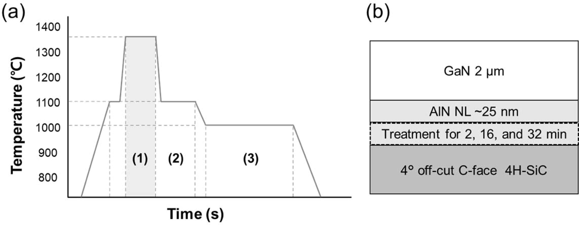
respectively. The pre-treatment time using NH3 was changed to 2, 16,
and 30 min for sample A, B, and C, respectively, and the temperature was set at
1,350 oC. Previously, it was found that the optimum treatment
temperature in our MOCVD system for growth of the N-polar GaN on SiC was
1,350 oC [11]. The temperature profile of the sample growth is
shown in Fig. 1(a). First, the SiC substrate was loaded into the reactor. The
air was removed and substituted with N2 for H2 injection.
Next, the substrate was heated to 1,100 oC for thermal cleaning
of organic residues using H2. The temperature was then increased to 1,350 oC
for NH3 surface treatment, varying from 2 to 32 min. After that, the
~25 nm-thick AlN nucleation layer (NL) was grown on the SiC substrate. Finally,
the 2 μm-thick GaN layer was grown on the AlN NL. The detailed de scription of
the sample growth conditions was addressed elsewhere
[11]. The sample structure is shown in Fig. 1(b). The polarity of the grown
layer was verified using 0.45M potassium hydroxide (KOH) aqueous solution at 80 oC for 5 min, and it was
confirmed that the layer successfully
grew into nitrogen polarity [11]. In addition, Ga-polar GaN sample was also
grown on on-axis Si-face SiC using
the growth condition of sample A to compare epi-layer characteristics. The
scanning transmission electron
microscopy high-angle annular dark-field imaging (STEM-HADDF, JEM-2100F with Cs
corrector, JEOL/CEOS) with 200 keV accelerating voltages was utilized to verify the structural property of the epitaxially grown layer at the
interface. Using focused ion beam (FEI, Quanta 3D FEG), 70-nm-thick samples
were prepared for the TEM measurement. The optical microscopy (Nikon, Eclipse
LV 150), the field-emission scanning
electron microscopy (Hitachi, S-4000)
with an accelerating voltage of 15
kV, the high resolution X-ray
diffraction (Panalytical, X’Pert Pro), low-temperature photoluminescence system
(Dongwoo optron) using 325 nm He-Cd laser (Kimmon) and liquid He cryostat, and the atomic force microscopy (Park
systems, XE-7) with a non-contact mode were used for
evaluating the hillock density, determining the etch rate,
evaluating the crystallinities and structural properties, and
measuring the surface roughness, respectively.
|
Fig. 1 (a) Temperature profiles (1) NH3 pre-treatment at 1,350 oC for 2, 16, and 32 min of sample A, B and C, respectively, (2) AlN
nucleation layer growth, and (3) GaN growth step. (b) schematic image of sample structure. |
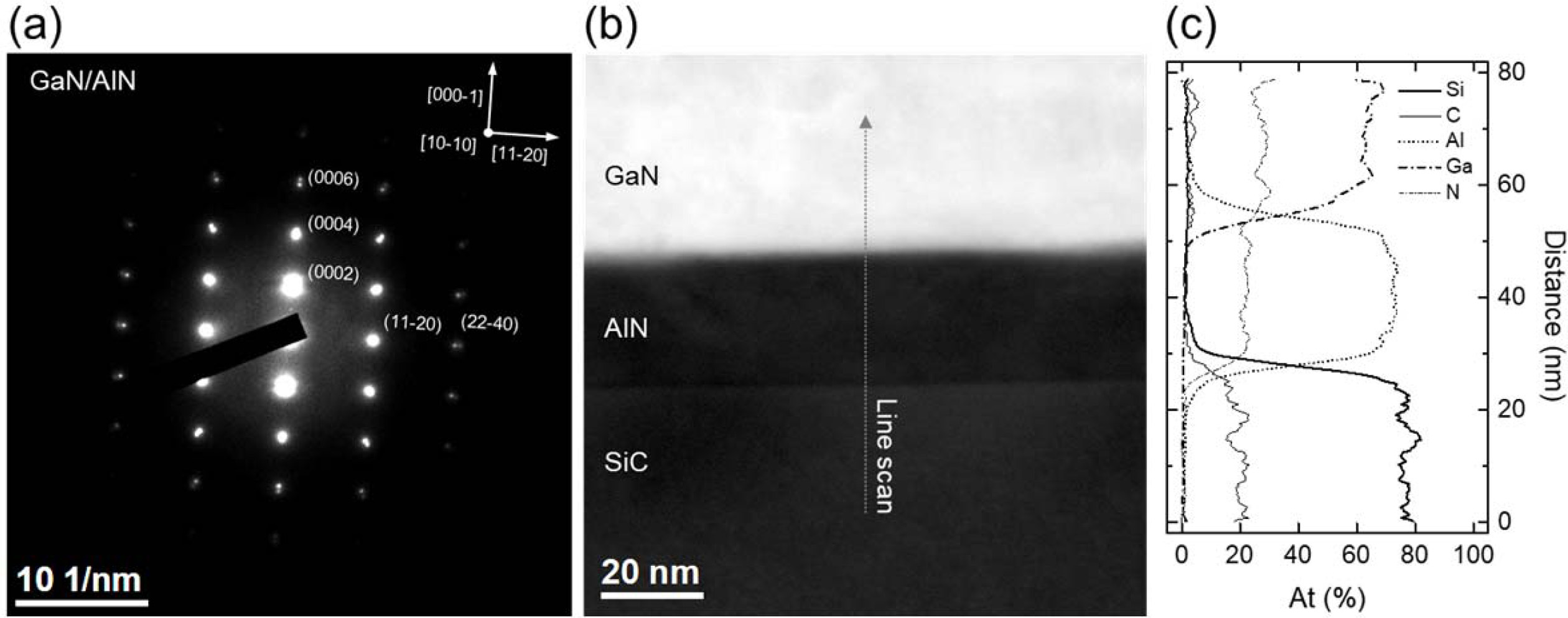
Three N-polar GaN samples with different pretreatment times of 2, 16, and 32 minutes,
respectively, were grown HT-MOCVD, and TEM measurement was conducted to verify
the structural property of sample A. Fig. 2(a) shows the selective area
electron diffraction (SAED) pattern with zone axis [10-10]SiC of
N-polar GaN/AlN NL/SiC structure indicating that the epi-layer structure
was successfully grown. The electron diffraction area was
carefully selected by focusing on the GaN/AlN interface. It was observed
that the diffracted patterns overlapped each
other owing to the very similar lattice constants between GaN and AlN [13].
However, in the case of farther points from center, reciprocal lattice points
(RLPs) can be distinguished in reciprocal space due to the smaller d-spacing.
The two RLPs in the third position
vertically measured distances of
~11.777 and ~11.404 nm-1,
respectively. In other words, the d-spacing of each point is 0.085 and 0.088
nm, respectively. These values were consistent with the one-sixth of lattice constant
values of AlN and GaN (cAlN = 4.98 Å, cGaN = 5.185
Å) while also having an error of just below 2% [13]. These TEM measurement
results were in good agreement with the XRD results (not shown here).
Therefore, it can be concluded that was reasonable to say that these RLPs are
the diffracted points of the epitaxially grown AlN and GaN layers. In the same
manner, the second RLPs in the horizontal direction measured the distances of
~12.580 and ~12.477 nm-1,
respectively. That is, the d-spacings
are 0.078 and 0.080 nm, respectively, which are identical values with the
d-spacing of the AlN and GaN (22-40) planes. Therefore, it can be said that the
epitaxial relationship of the GaN/AlN/SiC structure is (000-1)GaN //
(000-1)AlN // (000-1)SiC and [11-20]GaN //
[11-20]AlN // [11-20]SiC. Next, for the compositional
analysis, line profile of Energy-dispersive X-ray spectroscopy (EDX) was
obtained as shown in Fig. 2(b) and (c). The STEM-HADDF
image of the GaN/AlN/SiC structure (Fig. 2(b)) shows that the AlN
NL thickness is approximately 25 nm. Meanwhile, Fig. 2(c) shows the
line scan profile of GaN/AlN/SiC structure indicating the sharp interface
between them. The reason for the low atomic percentage of light elements such
as carbon and nitrogen can be attributed to poor signal generation and damage
caused by accelerated electrons [14].
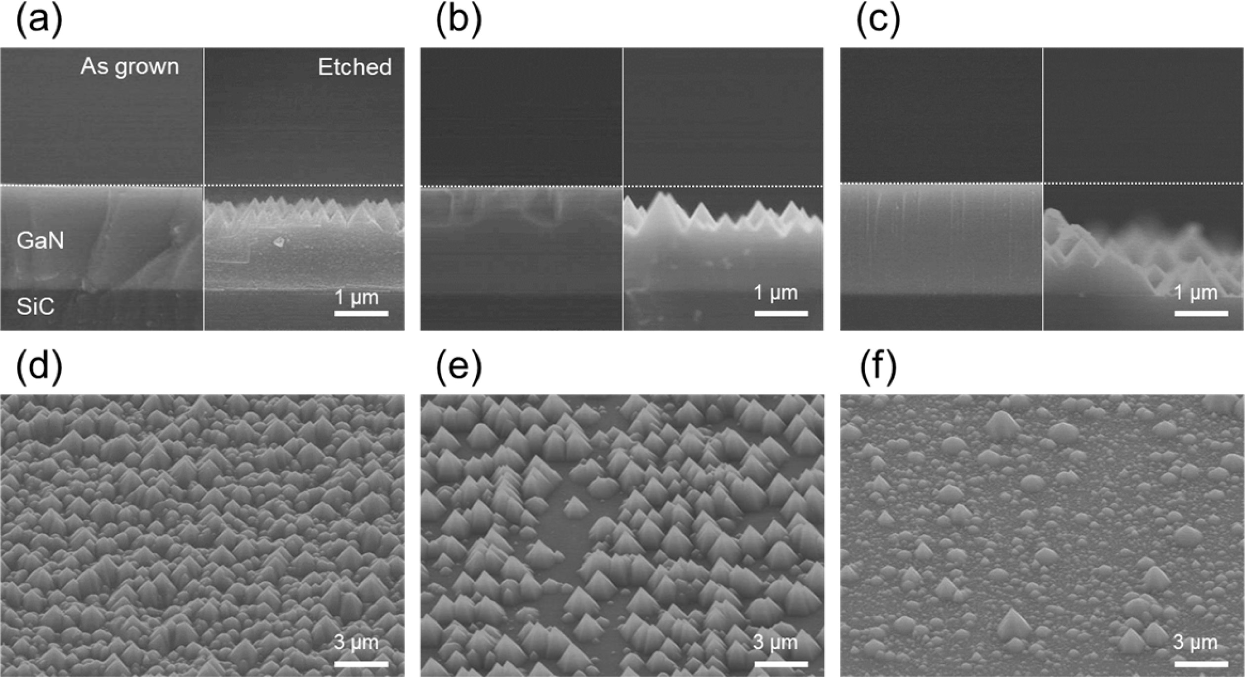
Fig. 3(a), (b), and (c) show the SEM cross-section images
(15k magnification) of sample A, B, and C before and after KOH wet etching,
respectively. The cross-section images show that the thicknesses of all samples
were identical at 2 μm KOH etched SEM image shows the triangular shaped
pyramids having the {11-10} plane which are verifying the N-polarity of the
samples [11]. It is worthy to note that the etched depth of each sample
differed with NH3 treatment time. This could be because the more
defective layers were etched deeper. However, it was shown that no difference
was observed before and after etching of the reference sample (not shown). Fig.
3(d), (e), and (f) show the bird’s eye view images (5k magnification) of the
wide surface area of etched samples. The surface coverage of N-polar hexagonal
hillock residue roughly decreased as the NH3 treatment time was
increased.
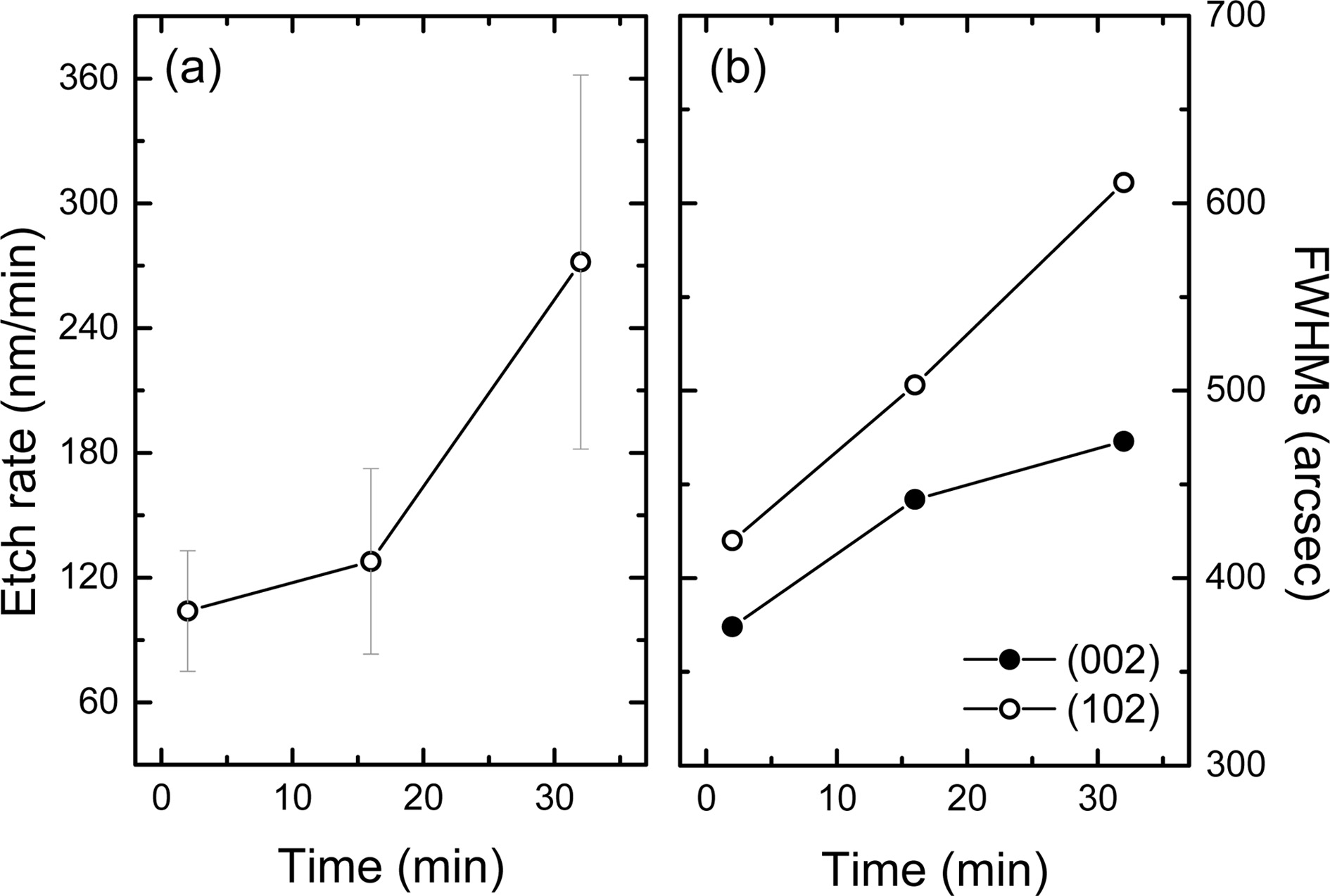
The measured etch rates are shown in Fig. 4(a). The etched
depth was obtained by averaging the peak and valley distances of the hexagonal
hillock from the surface of the as-grown samples. The etch rate of sample
A, B, and C was ~100, ~130, and ~270 nm/min, respectively.
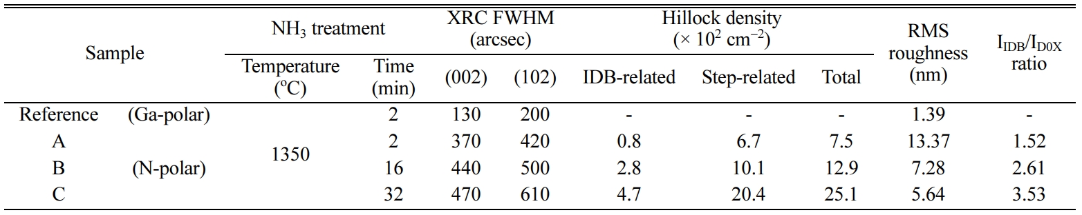
Fig. 4(b) shows the XRC FWHM trend for (002) and (102) planes of sample A, B,
and C. It was found that the FWHMs of (002) and (102) planes of sample A, B,
and C were 370 and 420, 440 and 500, as well as 470 and 610 arcsec,
respectively (Table 1). For reference sample, the FWHMs of each plane were 130
and 200 arcsec, and these results confirm the high crystal quality of the
Ga-polar GaN layer.
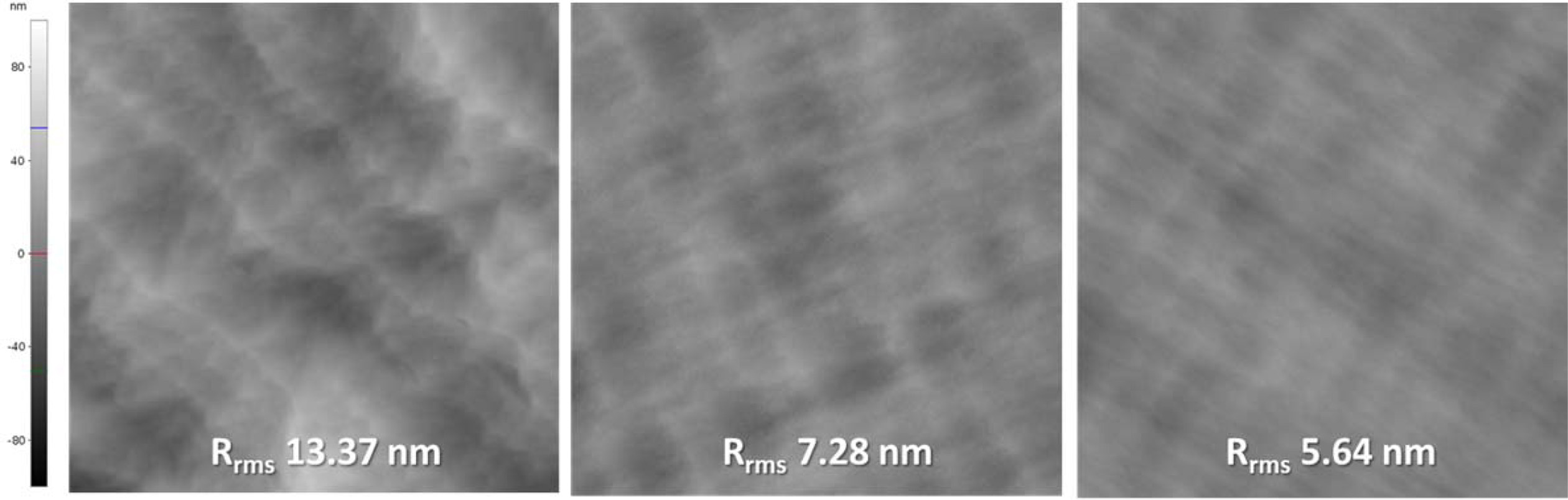
Fig. 5 shows the AFM scan results (20 × 20 μm2)
of sample A, B, and C. The root mean square (RMS) roughness of each sample was
13.37, 7.28, 5.64 nm, respectively as listed in Table 1. The surface flatness
improved as treatment time was increased. This can be due to the well-defined
step-terrace structure with increased treatment time, thus promoting step flow
growth [12,15,16].
However, this result contradicted the trend of XRC FWHMs.
The trade-off between crystal quality and surface roughness has been
extensively discussed in previous studies [17,18]. Although increased
treatment time promotes the step-flow growth mode of the N-polar GaN layer, it
should be noted that an excessively long treatment time could cause
unintentional reaction with the substrate, potentially causing surface damage.
For example, nitrogen in NH3 bonds easily to Si atoms at the surface
forming not only silicon nitride, but also silicon oxynitride when reacting
with oxygen [19]. As oxygen atom is one of the reasons for inverted polarity
resulting in inversion domain boundary (IDB) of N-polar nitride
film, the oxygen atoms in silicon oxynitride film at the surface
would lead to formation of the IDB [20]. In
our study, this assumption is the likely scenario, as the density of the IDB-related hexagonal increased with treatment
time. The density of hexagonal hillock of
sample A, B, and C were 0.8, 2.8, and 4.7 × 102 cm-2,
respectively (Table 1). In addition, Akiyama et al. reported that
the rapid change of the surface morphology of
the 6H-SiC substrate starts at 1,250 oC under hydrogen
atmosphere because SiC vaporized as SiHx and CHy due
to the reaction between SiC and H2 [21]. Moreover,
Zhang et al. reported the effects of treatment time on the surface morphology
of the c-sapphire substrate showing that longer treatment time had deteriorated
the surface morphology [22]. The altered terrace structure may affect the
step-related hillock formation due to its sensitivity to surface morphology
[10]. Similar to IDB-related hillock, the density of the step-related trigonal
hillock also increased with treatment time. The density of trigonal hillock of
each sample was 6.7, 10.1, and 20.4 × 102 cm-2,
respectively. That is, the total hillock density increased with the increase in
treatment time. The hillock density results do not match with the trend in
surface roughness results. It can be suggested that a longer treatment time
improves the overall terrace structure of the substrate but deteriorates in
partial regions. Meanwhile, the reference sample has RMS roughness of 1.39 nm,
which is smoother than that of N-polar GaN. Moreover, there was no evidence of
hillocks or surface defects observed.
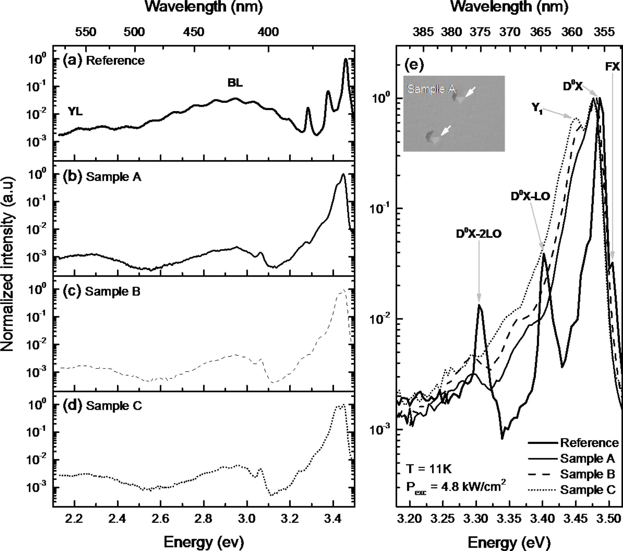
To investigate the optical properties of sample A, B, and
C, The LT-PL measurement was conducted at 11K. And Ga-polar GaN grown on
Si-face SiC was also measured at same condition. The laser power and diameter
was 13.7 mW and 20 μm. Figure 6 shows the stacked LT-PL spectra and enlarged
spectra. According to the stacked LT-PL spectra, broad blue luminescence (BL)
and yellow luminescence (YL) peaks were observed on all samples. BL band having
interference pattern on reference sample means transitions from the conduction
band or a shallow donor to a relatively deep acceptor [23]. or high quality GaN
films at low temperature
measurement. [24]. Fig. 6(e) shows the detailed spectra at
near-band edge emission. The D0X peak is the dominant emission at
near 3.48 eV in all samples including reference sample. In case
of reference sample, free-exciton peak that is shown at high quality
films is observed beside the D0X peak. The slight D0X
peak shift between reference and N-polar GaN sample series could be due to difference
in substrate off-cut [25]. The D0X-LO and 2LO peaks for the
reference sample were clearly identified. Contrary to the reference sample, Y1
(3.45 eV) peak was only detected in N-polar GaN samples indicating the
existence of IDB in the film [26]. Hexagonal hillock (white arrow) is in inset
optical microscope image, which is result of difference growth rate between
Ga-polar and N-polar [27]. The ratio of integrated intensities of IIDB/ID0X
for sample A, B, and C was 1.52, 2.61, and 3.53 respectively. The
intensity of these peaks was in accordance with the density of the hexagonal
hillock.
|
Fig. 2 (a) SAED pattern of GaN/AlN structure with zone axis of [10-10], (b) STEM image, and (c) EDX line scan profile of N-polar GaN/
AlN/C-face SiC structure. |
|
Fig. 3 Cross-sectional SEM images (15k magnification) of as grown and KOH etched GaN layers after NH3 treatment for 2 (a), 16 (b), and
32 min (c), and bird’s eye view images (5k magnification) of KOH etched GaN layer after NH3 treatment for 2 (d), 16 (e), and 32 min (f). |
|
Fig. 4 Etch rate of N-polar GaN using aqueous KOH (a) and XRC FWHMs of N-polar GaN layer with different treatment time (b). |
|
Fig. 5 AFM scan images (scan area 20 × 20 µm2
) of sample A (a), B (b), and C (c).. |
|
Fig. 6 Stacked LT-PL spectra of reference, sample A, B, and C ((a)-(d)) with grating/blaze 300/500 nm. The enlarged spectra of reference
and all samples (e) with grating/blaze 1200/250 nm. The inset OM image in (e) shows IDB-related hexagonal hillock of sample A (White
arrows) and scale bar is 50 µm. Measurement temperature (T) was 11K and laser excitation power (Pexc) was 4.8 kW/cm2
, respectively |
|
Table 1 XRC FWHMs, hillock density, surface RMS roughness, and PL IIDB/ID0X ratio of sample A, B, and C with different treatment
time. |
In conclusion, the effect of NH3 pretreatment
time on N-polar GaN growth on 4o off-cut C-face 4H-SiC was
investigated. We found that the NH3 pre-treatment time affects the
crystal quality. The Full width at half maximum (FWHM) of the (00-2) and (10-2)
plane of samples A, B, and C was 370, 440, and 470 arcsec, and 420, 500, and
610 arcsec, respectively. The hillock density related IDB of samples A, B, and C
was 0.8 × 10², 2.8 × 10², and
4.7 × 10², respectively, whereas the root-mean-square
(RMS) roughness values showed the tendency of decrease such as 13.7, 7.28, and
5.64 nm, respectively. This result is believed that the step flow growth can be
improved due to the well-defined step-terrace structure as the pre-treatment
time increase. From the PL measurement, only the N-polar GaN showed the Y1 peak
at 3.45 eV, which is due to IDB. The intensity of the Y1 peak is related to the
hillock because it is proportional to the pretreatment time. we expect that
this study offers a deeper understanding and a practical growth condition for
control in N-polar GaN epitaxy by applying NH3 pre-treatment time.
This work was supported by Civil-Military Technology
Cooperation Program 17-CM-MA-03
- 1. S. Pimputkar, J.S. Speck, S.P. Denbaars, and S. Nakamura, Nat. Photonics 3 (2009) 180-182.
-

- 2. S. Nakamura, M. Senoh, S.I. Nagahama, N. Iwasa, T. Yamada, T. Matsushita, H. Kiyoku, Y. Sugimoto, T. Kozaki, H. Umemoto, M. Sano, and K. Chocho, Appl. Phys. Lett. 73 (1998) 832-834.
-
- 3. M. Sun, Y. Zhang, X. Gao, and T. Palacios, IEEE Electron Device Lett. 38 (2017) 509-512.
-
- 4. T. Palacios, A. Chakraborty, S. Rajan, C. Poblenz, S. Keller, S.P. Denbaars, J.S. Speck, and U.K. Mishra, IEEE Electron Device Lett. 26 (2005) 781-783.
-
- 5. S. Keller, N. Fichtenbaum, F. Wu, G. Lee, S.P. Denbaars, J.S. Speck, and U.K. Mishra, Jpn. J. Appl. Physics, Lett. 45 (2006) 322-325.
-
- 6. M.H. Wong, S. Keller, N.S. Dasgupta, D.J. Denninghoff, S. Kolluri, D.F. Brown, J. Lu, N.A. Fichtenbaum, E. Ahmadi, U. Singisetti, A. Chini, S. Rajan, S.P. Denbaars, J.S. Speck, and U.K. Mishra, Semicond. Sci. Technol. 28 (2013) 074009.
-
- 7. S. Wienecke, B. Romanczyk, M. Guidry, H. Li, E. Ahmadi, K. Hestroffer, X. Zheng, S. Keller, and U.K. Mishra, IEEE Electron Device Lett. 38 (2017) 359-362.
-
- 8. B. Romanczyk, S. Wienecke, M. Guidry, H. Li, E. Ahmadi, X. Zheng, S. Keller, and U.K. Mishra, IEEE Trans. Electron Devices 65 (2018) 45-50.
-
- 9. F. Akyol, D.N. Nath, E. Gür, P.S. Park, and S. Rajan, Jpn. J. Appl. Phys. 50 (2011) 052101.
-
- 10. D. Won, X. Weng, and J.M. Redwing, Appl. Phys. Lett. 100 (2012) 021913.
-
- 11. U. Choi, K. Lee, J. Han, T. Jang, Y. Nam, B. So, T. Kwak, and O. Nam, Thin Solid Films 675 (2019) 148-152.
-
- 12. F. Yi, N. Xianfeng, X. Jingqiao, N. Biyikli, F. Qian, S. Chevtchenko, Ü. Özgür, H. Morkoç, K. You, R. Devaty, W.J. Choyke, C.K. Inoki, and T.S. Kuan, MRS Proceedings. 955 (2006) 0955.
-
- 13. O. Ambacher, B. Foutz, J. Smart, J.R. Shealy, N.G. Weimann, K. Chu, M. Murphy, A.J. Sierakowski, W.J. Schaff, L.F. Eastman, R. Dimitrov, A. Mitchell, and M. Stutzmann, J. Appl. Phys. 87 (2000) 334-344.
-
- 14. A. Meingast, in “Analytical TEM Investigations of Nano- scale Magnetic Materials” (Graz Univertsity of Technology, 2015) 86.
- 15. J.T. Torvik, M.W. Leksono, J.I. Pankove, C. Heinlein, J.K. Grepstad, and C. Magee, J. Electron. Mater. 28 (1999) 234-239.
-
- 16. S. Yamada, J.I. Kato, S. Tanaka, I. Suemune, A. Avramescu, Y. Aoyagi, N. Teraguchi, and A. Suzuki, Appl. Phys. Lett. 78 (2001) 3612-3614.
-
- 17. Y. Lin, S. Zhou, W. Wang, W. Yang, H. Qian, H. Wang, Z. Lin, Z. Liu, Y. Zhu, and G. Li, J. Mater. Chem. C 3 (2015) 1484-1490.
-
- 18. Z.Y. Al Balushi and J.M. Redwing, J. Mater. Res. 30 (2015) 2900-2909.
-
- 19. E. Pitthan, A.L. Gobbi, H.I. Boudinov, and F.C. Stedile, J. Electron. Mater. 44 (2015) 2823-2828.
-
- 20. D. Won and J.M. Redwing, J. Cryst. Growth 377 (2013) 51-58.
-
- 21. K. Akiyama, Y. Ishii, S. Abe, H. Murakami, Y. Kumagai, H. Okumura, T. Kimoto, J. Suda, and A. Koukitu, Jpn. J. Appl. Phys. 48 (2009) 095505.
-
- 22. D. Zhang and Y. Gan, Appl. Surf. Sci. 285 (2013) 211-214.
-
- 23. M.A. Reshchikov and H. Morko̧, J. Appl. Phys. 97 (2005) 061301.
-
- 24. M.A. Reshchikov, F. Shahedipour, R.Y. Korotkov, B.W. Wessels, and M.P. Ulmer, J. Appl. Phys. 87 (2000) 3351-3354.
-
- 25. D. Won, X. Weng, Z.Y. Al Balushi, and J.M. Redwing, Appl. Phys. Lett. 103 (2013) 241908.
-
- 26. M.A. Reshchikov, J. Jasinski, Z. Liliental-Weber, D. Huang, L. He, P. Visconti, and H. Morkoç, Phys. B Condens. Matter 340-342 (2003) 440-443.
-
- 27. L.T. Romano and T.H. Myers, Appl. Phys. Lett. 71 (1997) 3486-3488.
-
 This Article
-
2020; 21(5): 579-585
Published on Oct 31, 2020
- 10.36410/jcpr.2020.21.5.579
- Received on May 1, 2020
- Revised on Jun 19, 2020
- Accepted on Jul 16, 2020
Services
- Abstract
introduction
experimental details
results and discussion
conclusion
- Acknowledgements
- References
- Full Text PDF
Shared
Correspondence to
- Okhyun Nam
-
Nano-Optical Engineering, Korea Polytechnic University (KPU), Siheung, Gyeonggi 427-793, Republic of Korea
Tel : +82-31-8041-0718
Fax: +82-31-8041-0729 - E-mail: ohnam@kpu.ac.kr
Clean-Energy Research Institute(CRI), Hanyang University, 222, Wangsimni-ro, Seongdong-gu, Seoul, 04763, Korea
E-mail: jcpr@hanyang.ac.kr