


- Fabrication of silicon carbide particles from recycled polysilicon photovoltaic cells
Ah Hyun Oha,†, Hyeon Seung Leea,†, Bong-Gu Kimb, Sung-Churl Choia, Yeon-Gil Jungb and Gye Seok Ana,*
aDivision of Materials Science and Engineering, Hanyang University, 222 Wangsimni-ro, Seongdong-gu, Seoul 04763, Republic of Korea
bSchool of Materials Science and Engineering, Changwon National University, 20 Changwondaehak-ro, Changwon, Gyeongnam, 51140, Republic of Korea
In this study, a recycling
method for the recovery of polysilicon (poly-Si) wafers from end-of-life
poly-Si photovoltaic (PV) cells and the synthesis of high-purity silicon
carbide (SiC) using the recovered poly-Si wafers are reported. First, an
end-of-life poly-Si PV module was etched by acid treatment, using a mixture of
hydrofluoric acid (HF) and nitric acid (HNO3), to recover the
poly-Si wafer. The purified wafer was milled using high-energy milling to form
Si powders to prepare a fine SiC powder. Then, the SiC powder was synthesised
using spark plasma sintering with a mixture of poly-Si powder and carbon black.
By analysing the morphology and crystal structure of the SiC powders
synthesised at different reaction temperatures, the optimum temperature for
synthesising the fine SiC powder was determined. After milling, the poly-Si and
SiC powders were washed using a HF solution to remove the oxide impurities from
the powders. Thus, a fine SiC powder with an oxygen content of 0.11% was
obtained.
Keywords: Polysilicon photovoltaic cell, Recycle, High-energy milling, Silicon carbide, Spark plasma sintering
Photovoltaics (PVs) have received significant attention
as a renewable energy source; thus, deployment of solar modules has rapidly
increased [1]. However, PV modules have a limited lifetime of 25–30 years.
Hence, with the rapid deployment of PV modules, an increase in waste modules is
expected [2]. Generally, the end-of-life PV modules are landfilled or
incinerated, which can lead to serious environmental pollution [3,4]. To solve
this problem, various recycling methods for unserviceable PV modules have been
proposed.
In particular, the recycling of polysilicon (poly-Si)
wafers in poly-Si PVs has been actively researched following the increase in
industrial application and transition to other materials, particularly silicon
carbide (SiC), which has attracted significant attention. Cubic-structured SiC
is a ceramic carbide material with strong covalent
bonds that possesses high mechanical strength, hardness,
thermal conductivity, thermal shock resistance, good
corrosion resistance, and semi-conductivity [5–7]. Therefore, it has been used
in various industrial appli- cations
such as in semiconductors, heating elements, and extreme-environment materials
[8]. Because SiC exhibits its superior characteristics when in the form of fine
powders, the demand for fine SiC powders have steadily increased. Therefore,
fabrication of fine SiC powders using poly-Si wafers recovered
from end-of-life poly-Si PV cells offers significant industrial
potential.
In this study, fine SiC powder
was synthesised using poly-Si wafers recovered from an end-of-life poly-Si PV
cell. To obtain high-quality poly-Si wafers, the poly-Si PV cell was etched
using mixed acid consisting of hydrofluoric acid (HF) and nitric acid (HNO3).
The recovered poly-Si wafer was milled using a high-energy mill and washed with
an HF solution to remove the oxide impurities produced during milling. In the
process, the oxide-impurity removal efficiency, which depended on the HF
concentration, was investigated. SiC was synthesised by making the Si powder
react with carbon using spark plasma sintering (SPS), which could reduce the
synthesis time and minimise particle growth [9,10]. The effect of synthesis
temperature was examined by investigating the crystal phase and morphology. The
synthesised SiC was washed several times using an HF solution, and the
oxide-removal efficiency was investigated.
Recovery
of poly-Si wafer
The poly-Si wafer was recovered from a poly-Si PV cell
using acid treatment. The acid treatment was performed using a mixed acid
consisting of HF (49%–52%, Duksan Pure Chemicals Co. Ltd., Korea) and HNO3
(60%–62%, Junsei Chemical Co., Ltd., Japan). The poly-Si PV cell
(SH-1880S3N-M, 6", Shinsung Solar Energy Co., Ltd., Korea) was immersed
into 1 L of the mixed acid, which was prepared by mixing HF, HNO3,
and water in a volume ratio of 5:30:65 and etched for 15 min at 80 oC
on a hot plate. Then, the etched cell was washed several times and dried at
60 oC for 1h in a vacuum drying oven.
Grinding
and washing of poly-Si wafer
The recovered poly-Si wafer was initially crushed using a
zirconia mortar for 2 h. Subsequently, it was put into a SiC jar
(48 × 51 mm, laboratory grade) with a SiC ball
(10 mm in diameter) whose weight depended on the ball-to-powder
ratio (BPR) of 2.55:1. Thereafter, the Si powder was pulverised in a SPEX mill
(8000D, SPEX SamplePrep, USA), which can provide high impact energy to the
powder by increasing the milling time from 2 to 20 h. After milling, the
0.5 g of Si powder was washed with 40 mL of 1 wt%–5 wt% HF
solution and water several times. Then, the powder was dried at 70 oC
for 6 h under a vacuum pressure of 1 × 10⁻² Torr in a
vacuum drying oven.
Synthesis
of SiC powder
To synthesise SiC, the as-prepared Si powder and carbon
black (99.9%, Alfa Aesar, USA) were used as the initial materials for Si and C,
respectively. Si and the carbon black powder were mixed at a 1:1.8 molar ratio
using a ball mill for 48 h at 200 rpm in a polypropylene
bottle with SiC balls (10 mm in diameter) with an
adjusted BPR of 10:1. The mixed powder was pressed by 12.5-MPa pressure in a
graphite die (inner diameter: 12.7 mm). The graphite die was installed in
the SPS furnace (EL tek Korea, Korea) and treated under 30 MPa pressure in
vacuum at the temperature range of 1200–1400 oC (heating rate:
100 oC/min) for 1 h. The synthesised SiC was crushed by
the SPEX mill for 2 h using a 10-mm-diameter SiC ball and pulverised by a
sieving process. Then, 0.5 g of SiC powder was
washed several times with 40 mL of 5 wt% HF solution
and water and subsequently dried at 70 oC for 6 h in a
vacuum dryer under 1 × 10⁻² Torr of vacuum pressure in a
vacuum drying oven.
Characterisation
The morphologies and compositions of the wafer and
particles were analysed using field emission scanning electron microscopy
[(FE-SEM), JSM-6330F, JEOL, Japan] and energy-dispersive spectroscopy [(EDS),
EDAX detector (DPP-II), USA], respectively. The elemental composition of the
recovered Si wafer was quantitatively analysed using glow-discharge mass spectrometry
[(GDMS), GD90RF, Msi, UK]. The particle size of the
milled Si powder was measured using the dynamic light scattering (DLS) method
(Zetasizer Nano ZS, Malvern, USA). The changes in the oxygen contents that
remained in the Si and SiC powder were measured using a nitrogen/oxygen
determinator (TC-600, LECO Co., USA). The crystal structure of the synthesised
SiC particle was analysed by X-ray diffraction [(XRD),
Ultima IV, Rigaku, Japan] with Cu–Kα radiation (λ = 1.5418 Å).
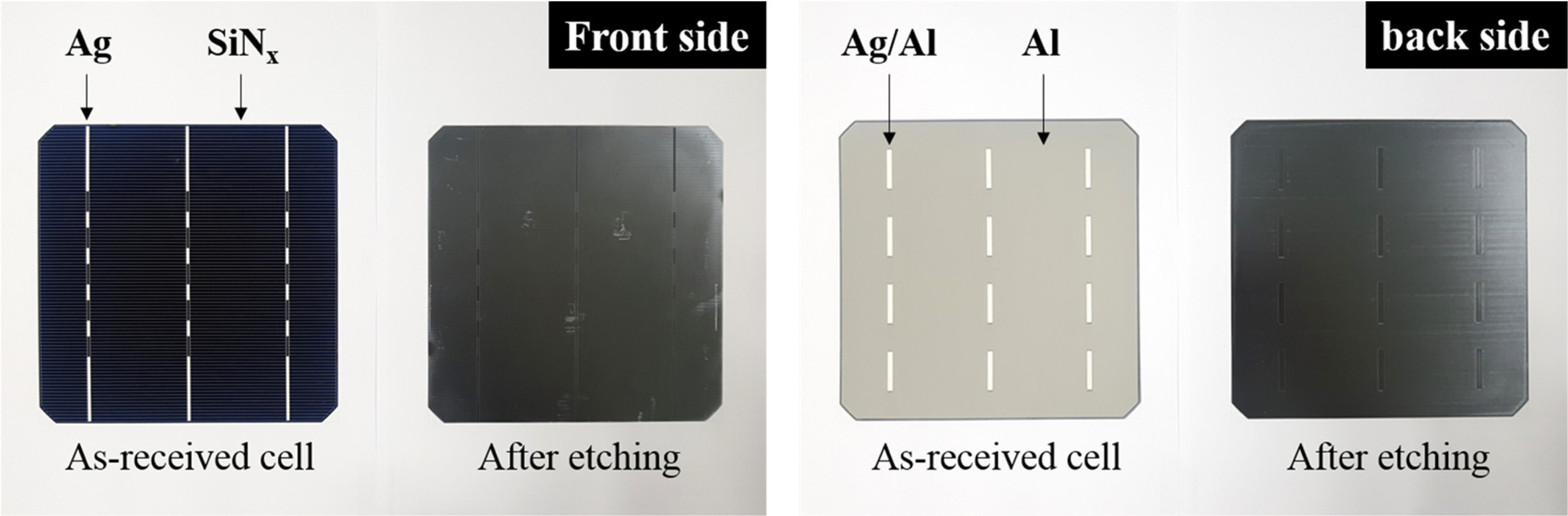
The photographic images of the front and back sides of the
poly-Si PV cell before and after etching are shown in Fig. 1. Before etching,
the front side showed the deposition of a blue SiNx anti-refracting
coating layer and Ag electrode. After etching by the acid treatment, the Ag
electrode was removed from the surface of the PV cell; however, an
indentation remained in its place. Similarly, the SiNx
anti-refracting coating layer was removed, leaving a stripe mark at its
original position. Additionally, some random scratches were observed at the
front side of the etched PV cell, which were presumed to occur due to the
friction between the PV cell and tray during the etching process. On the other
hand, the back side of the PV cell exhibited a white line corresponding to the
Ag/Al soldering pad and Al-back surface field. Similar to the case at the front
side, the Ag/Al soldering pad on the back side disappeared after the acid
treatment, leaving behind an indentation. In addition, the Al-back surface
field was removed, and line marks, which were assumed to be generated during
the production of poly-Si wafer, were left in the back field. Overall, Ag, Al,
and SiNx appeared to have been eliminated from the front and back
sides of the etched PV cell, and only the poly-Si remained.
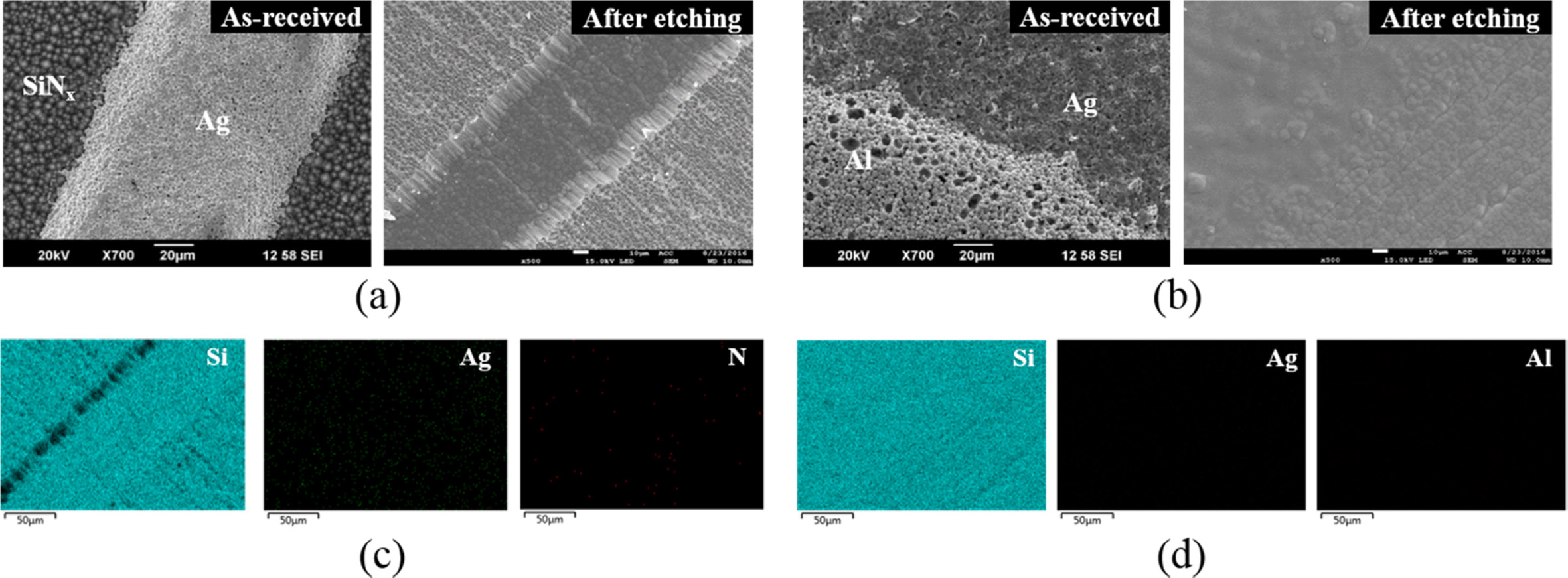
SEM was performed to observe the changes in the morphology
before and after etching, and EDS was simultaneously performed for qualitative
analysis of the etched PV cell (Fig. 2). Before etching, the front side of the
as-received PV cell showed aggregated SiNx and Ag particles along
the SiNx anti-reflecting coating layer and Ag electrode area,
respectively [Fig. 2(a)]. After the etching, the aggregated particles
disappeared, and an indentation was left in place of the Ag electrode. After
the etching, the aggregated particles disappeared, and an indentation was left
in place of the Ag electrode. SiNx and Ag reacted with HF and HNO3
in the acid solution as follows:
Ag + 2HNO3 → AgNO3 + NO2 + H2O
reaction (1)
Si3N4 + 16HF → 2(NH4)2SiF6 + SiF4 reaction (2)
According to reactions (1) and (2), SiNx and Ag
were detached from the front of the PV cell due to vaporisation or dissolution
into the solution in an ionised state. Similarly, the back [Fig. 2(b)]
exhibited aggregated Ag and Al particles along the Ag/Al soldering
pad and Al back-surface-field area, respectively, before
etching. After the etching, the area comprising the aggregated particles was
eliminated, and slight line marks were left in place of Al. The Ag, which was
deposited as a soldering material, reacted with the acid solution according to
reaction (1), whereas the Al in the back-surface field reacted according to
reaction (3).
2Al + 6HF → 2AlF3 + 3H2
reaction (3)
Because of these reactions, Ag and Al could be separated
in the gas or ionised state in the acid solution. The removal of the deposited
materials by the acid treatment was confirmed from the EDS mapping results. The
EDS data indicated the removal of the Ag electrode and SiNx coating
layer from the front side [Fig. 2(c)] and Ag/Al soldering pad and Al back
surface field from the back side [Fig. 2(d)], which exposed the Si wafer.
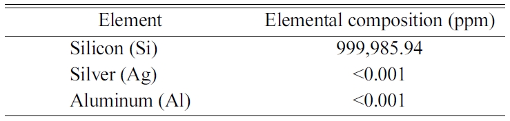
The elemental composition of the etched poly-Si PV cell
was analysed using GDMS, and a summary of the contents of the main elements is
listed in Table 1. After the etching, the Si
content was 999985.94 ppm (99.998594%), which implied high purity. On the
other hand, the Ag and Al contents, which were deposited as the electrode and
back-field layer, respectively, were below 0.001 ppm (0.0000001%), which
was beyond the measurable range of the GDMS. These results suggested that the
poly-Si wafer recovered from the poly-Si PV cell was highly pure and almost
free of impurities; hence, the recovered poly-Si could be used as a starting
material for high-purity SiC.
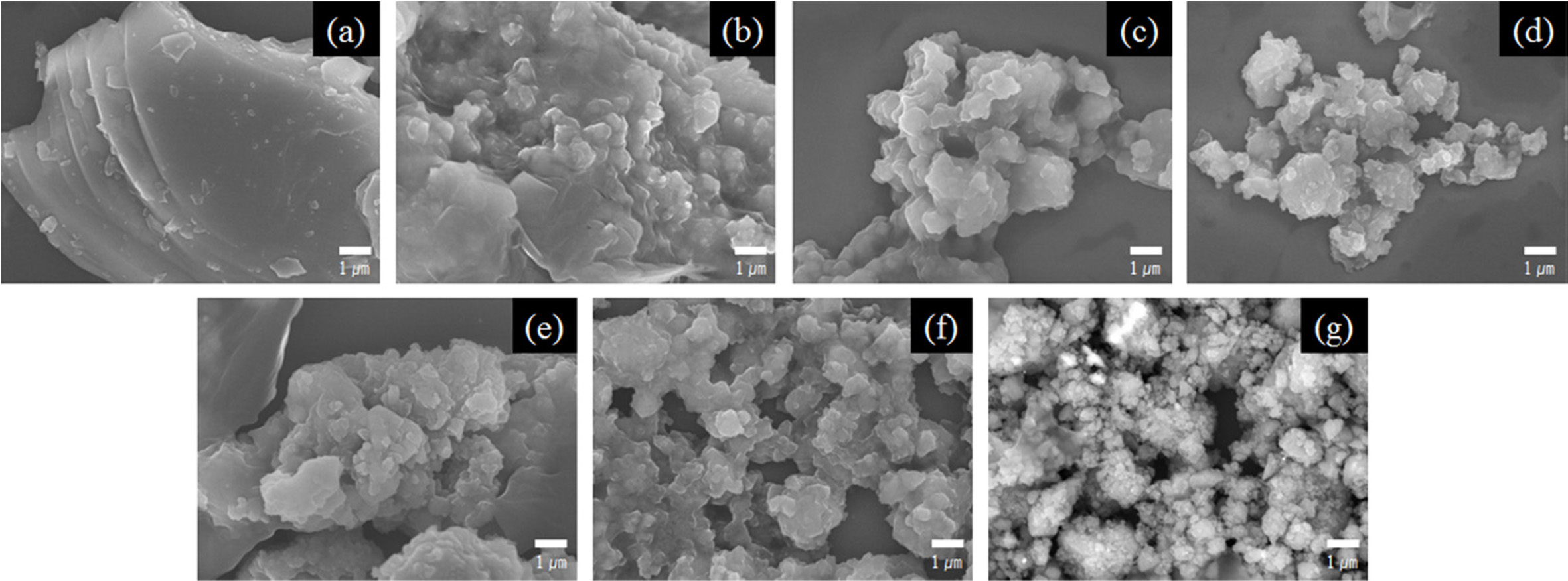
Fig. 3 shows the SEM images of the poly-Si wafer obtained
by varying the milling time. The initial hand-ground Si wafer [Fig. 3(a)]
contained a layered and microsized plate structure. The plate structure, which
had the characteristic of poly-Si wafers, could not be transformed into other
shapes by hand grinding using a mortar. When the Si wafer was milled for
2 h using the SPEX mill, a small amount of the plate structure remained,
and the milled particles aggregated [Fig. 3(b)]. After 4 h of milling, the
plate structure of the Si wafer almost disappeared [Fig. 3(c)]. The transfor- mation of the individual particles started
after 6 h of milling. Beyond this time, the particle size of the Si powder
steadily decreased with the increase in the milling time [Fig. 3(d)]. The
particle size continued to decrease and was finally reduced to the nanoscale
size after 20 h of milling [Fig. 3(g)].
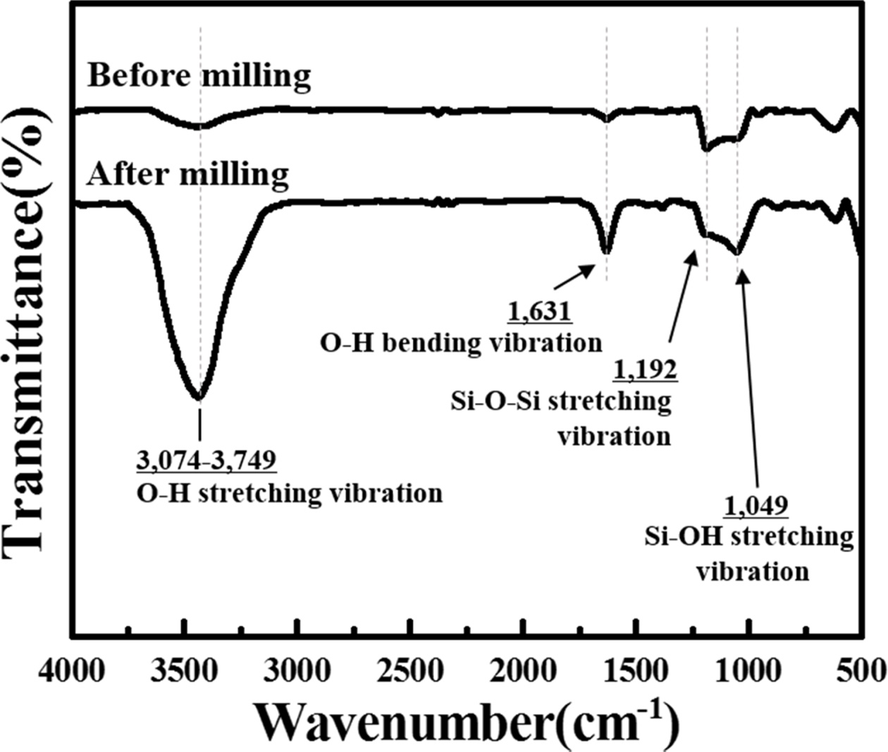
Meanwhile, some impurities appeared in the poly-Si
particles milled using the SPEX mill. To identify the impurities, the surface
functional groups of the Si wafer, which were hand-ground and SPEX-milled for 10 h,
were investigated using Fourier transform infrared (FT-IR)
spectroscopy (Fig. 4). The O–H stretching and bending
vibration peaks were observed at approximately
3,074–3,749 cm−1 and 1631 cm−1, respectively,
because of the presence of the hydroxyl group (Si–OH) in all samples [11–13].
Additionally, siloxane (Si–O–Si) and silanol (Si–OH) functional groups appeared
at 1,192 and 1,049 cm−1, respectively [14, 15]. The absorption peak
intensities of the SPEX-milled Si wafer over the entire wavenumber range were
much higher than those of the Si wafer before milling, which indicated that the
oxidation of Si occurred even before milling. However, the oxidation
significantly progressed after milling. As a result, SiO2 was formed
on the Si powder because SiO2 was dominantly generated from the Si
oxidation.
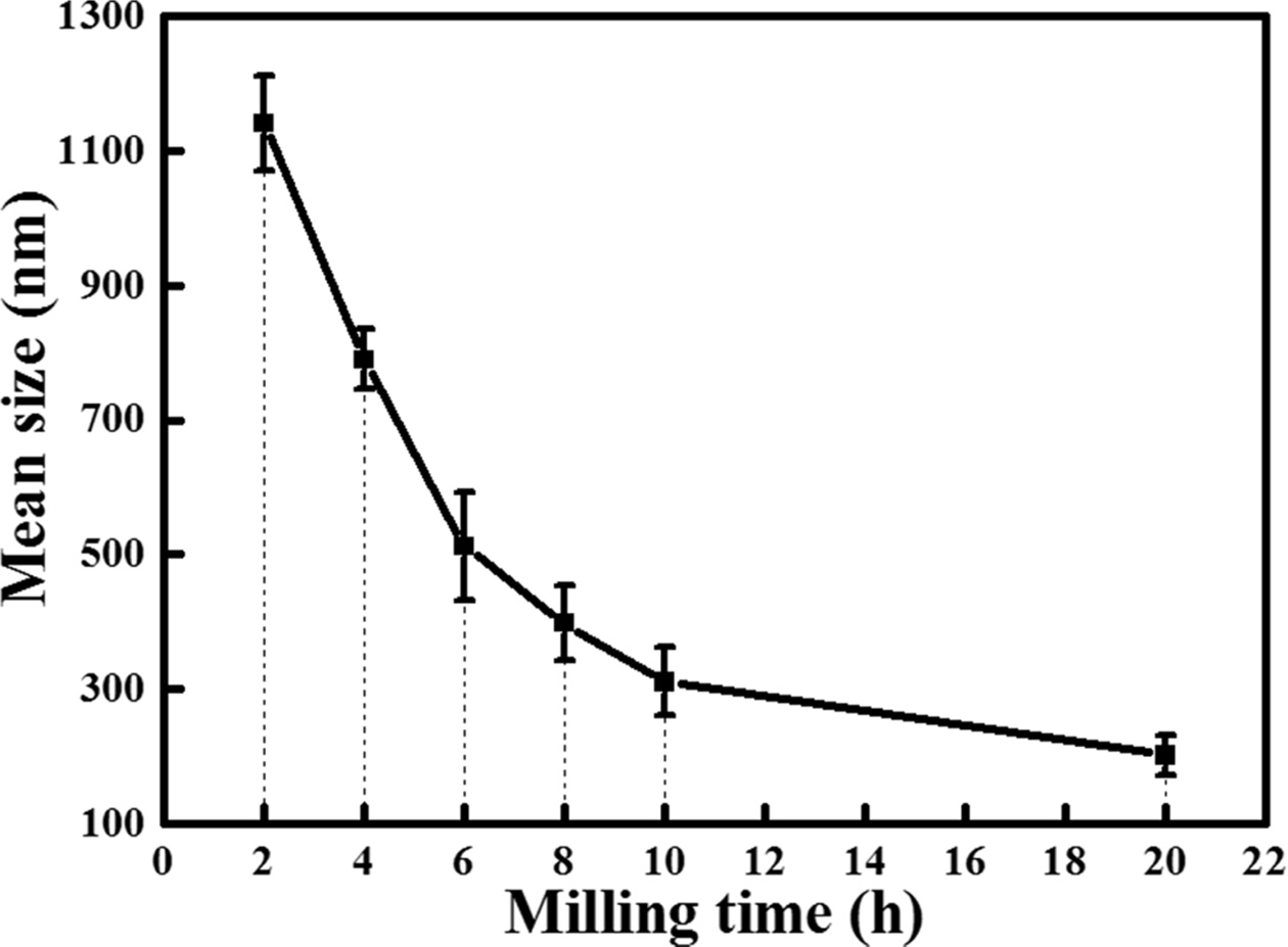
The average particle size of the poly-Si wafer
investigated using the DLS method with varying milling time is shown in Fig. 5.
Each sample was measured five times. As shown, the particle size decreased with
the increase in the milling time. After 2 h of milling, the average
particle size of poly-Si was 1.14 µm and decreased to 790 nm at
4 h of milling. The average particle size steadily decreased to 512, 398,
and 311 nm after 6, 8, and 10 h of milling, respectively. This
tendency continued up to 20 h of milling; at this stage the average
particle size was 202 nm. Furthermore, the standard deviation of the particle
size of the milled powder decreased from 70 to 30 nm after 20 h of
milling. Therefore, milling resulted not only in particle-size reduction, but also
in particle-size homogeneity.
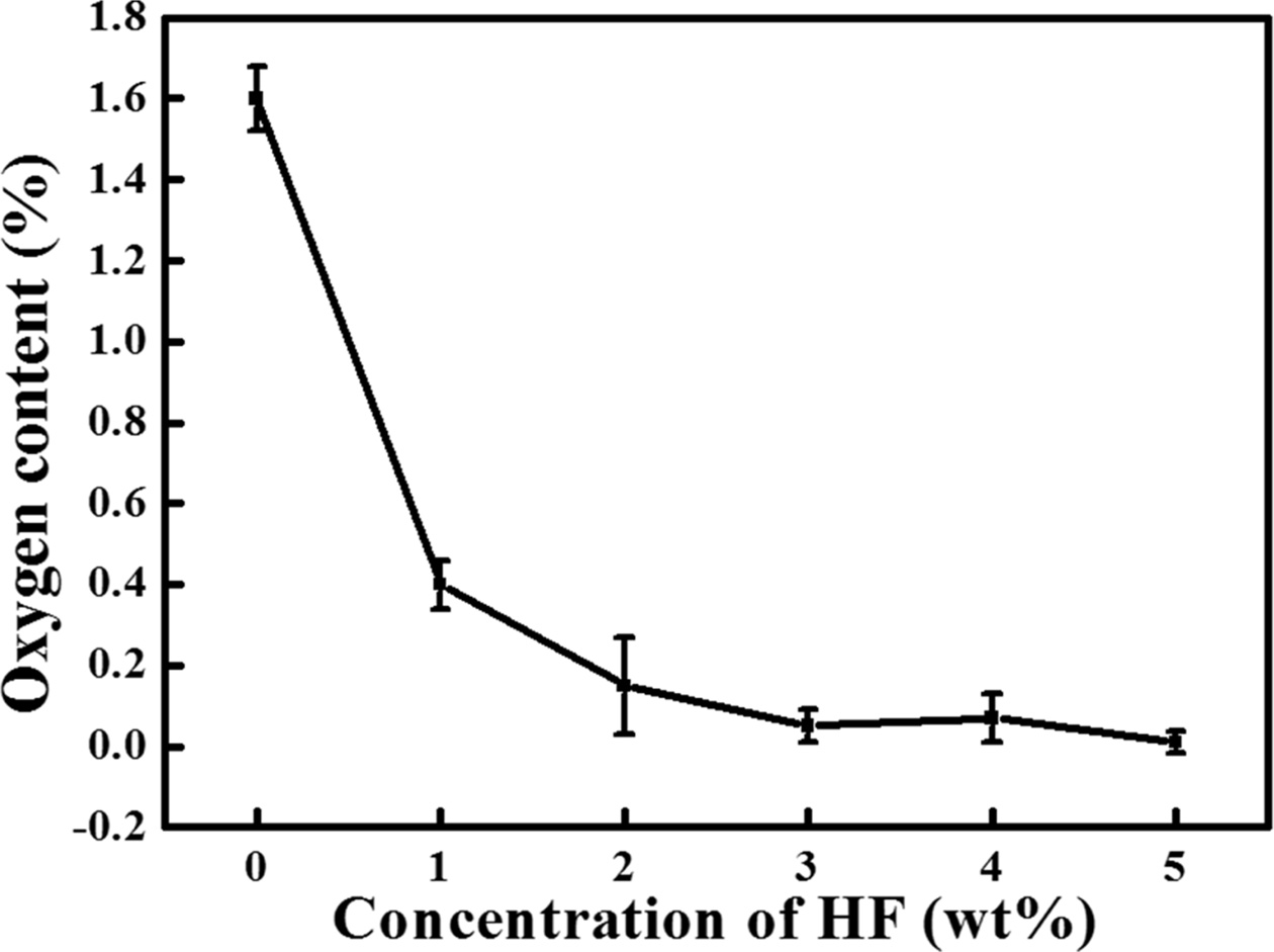
To remove the SiO2 that was formed during the
milling of poly-Si wafer, the Si powder was washed with HF solution. SiO2
reacted with HF as follows:
SiO2 + 4HF → SiF4 + H2O
reaction (4)
SiO2 + 6HF → H2SiF6 + 2H2O
reaction (5)
According to reactions (4) and (5), SiO2
reacted with HF to produce H2O and SiF4 gas or ionised H2SiF6,
which could be removed from the surface of the Si particles. A dilute HF
solution with a concentration in the range of 1–5 wt% was used, and washing
was performed using 40 mL of HF solution per 0.5 g of milled Si
powder. The oxygen content of the Si powder according to the HF concentration
of the washing solution is shown in Fig. 6. The oxygen content of the poly-Si
particles before washing was 1.6% and decreased to 0.4%
when washed with 1 wt% HF solution. With the increase in the HF
concentration from 2 wt% to 5 wt%, the oxygen content of the Si powder
decreased to 0.15%, 0.05%, 0.07%, and 0.01%, respectively. Thus, the oxygen
content decreased depending on the HF concentration in the washing solution.
Additionally, 3 wt% HF could be considered as the optimal con- centration because the oxygen content
sharply dropped at 3 wt% HF, and only slight changes were observed at
higher concentrations. However, because the standard deviation was 0.04% at
3 wt% and 0.026% at 5 wt%, the 5 wt% concentration with a low
standard deviation was considered as the optimal HF concentration.
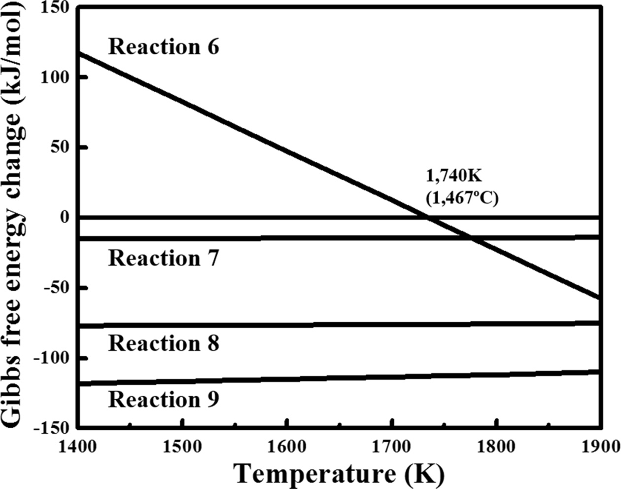
Table 2 lists the synthesis routes to SiC and the Gibbs
free-energy change corresponding to the reactions [16, 17].
Fig. 7 shows a summary of the Gibbs free energy of the reaction listed in Table
2. When SiO2 was used as a Si source, SiC was synthesised by
reaction (6) in which SiO2 and C reacted to form SiC and gaseous CO.
Because the calculated thermodynamic reaction temperature of reaction (6) was
1735 K (1462 oC), the reaction occurred at a temperature
higher than 1735 K (1462 oC). Meanwhile, in the present
study, the possible reactions were assumed as reactions
(7) and (8) because a previously recovered Si powder was directly
used. In addition, reaction (9), which combined reactions (7) and (8), was
considered to be dominant during the synthesis. The change in the
Gibbs free energy in reaction (9) had a negative value in the temperature
range of 1400–1900 K; thus, SiC synthesis was considered possible in the
temperature range of 1473–1673 K (1200–1400 oC), which was
lower than that for the reaction using SiO2.
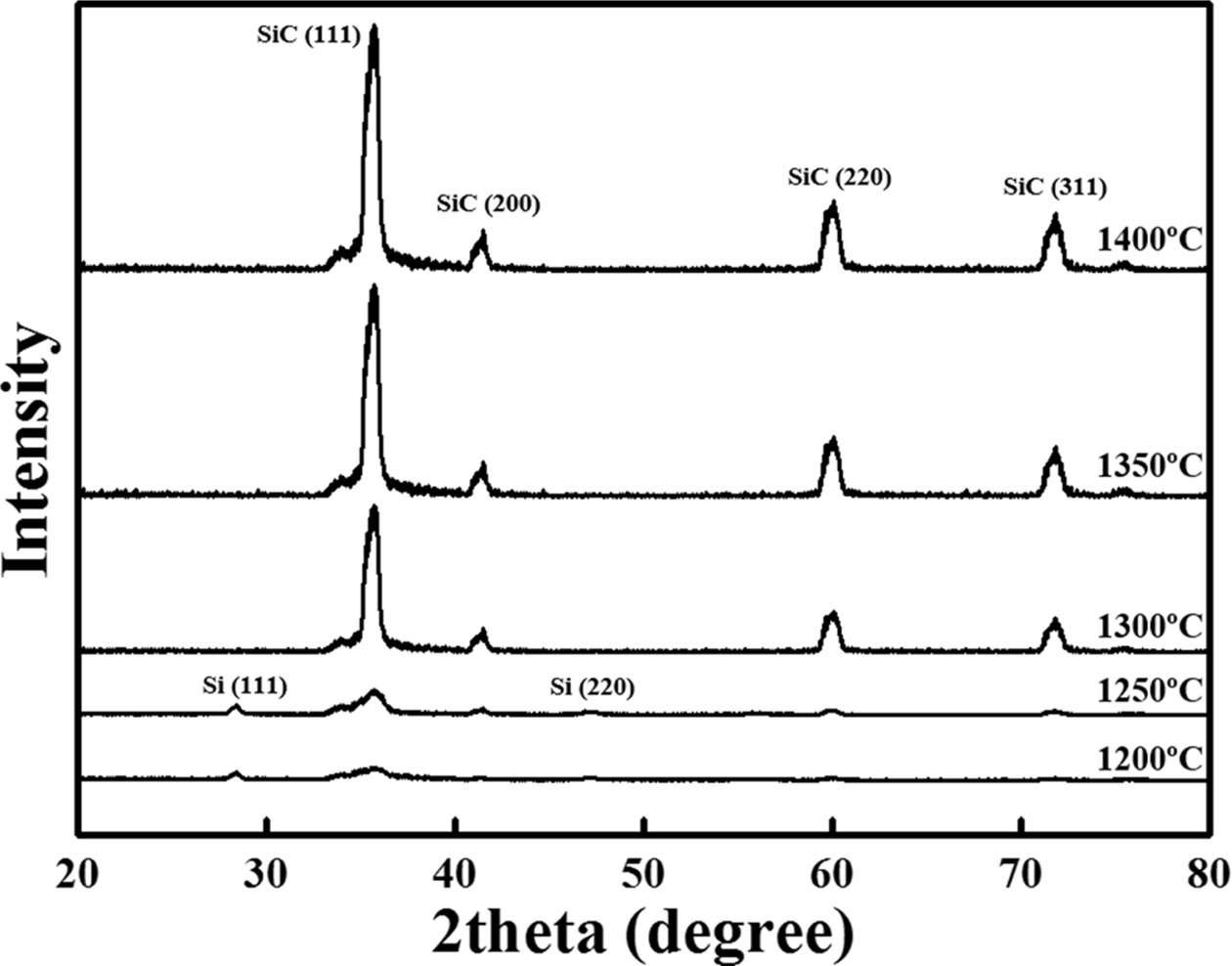
The SiC samples were synthesised by SPS using a mixture of
Si and carbon black at a molar ratio of 1:1.8 in the temperature range of
1200–1400 oC. The XRD profiles of the samples are shown in Fig.
8. In the case of the samples synthesised at temperatures above 1300 oC,
diffraction peaks appeared at 35.64°, 41.26°, 60.08°, 71.82°, and 74.72°
corresponding to the (111), (200), (220), (311), and (222) planes
of SiC, respectively (JCPDS #73-1665) [18]. On the other hand, in the
samples synthesised at 1200 and 1250 oC, diffraction peaks
appeared at 28.42° and 46.92° corresponding to the (111) and (220) planes of Si
and SiC, respectively (JCPDS #27-1402) [19]. However, the low intensity of Si
and SiC peaks indicated a low degree of crystallisation; thus, the
crystallinity was considered uncertain. These results
indicated that a temperature of 1300 oC or higher
is required for the synthesis of crystalline SiC [17].
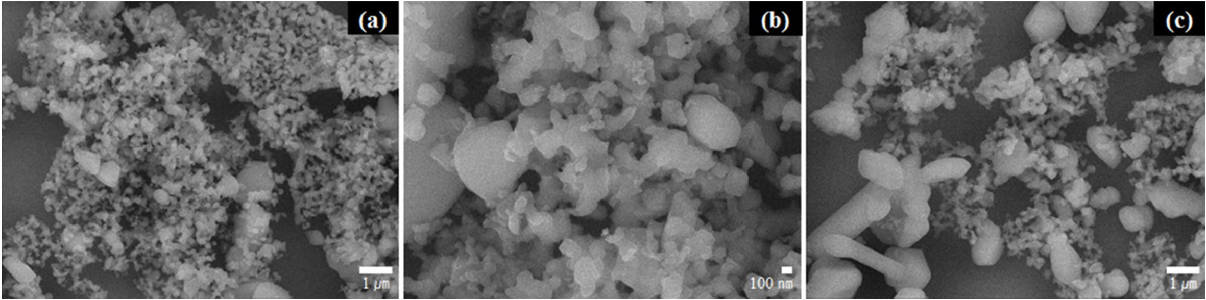
Fig. 9 shows the SEM images of the SiC synthesised in the
temperature range of 1300–1400 oC. Crystalline SiC was formed
in all the investigated temperatures; however, the particle size gradually
increased with the increase in temperature. The SiC synthesised at 1300 oC
contained particles with sizes in the range of 200–300 nm [Fig. 9(a)],
whereas SiC synthesised at 1350 oC had larger particles [Fig.
9(b)]. At 1400 oC, the particles grew to a size of
approximately 2–3 µm [Fig. 9(c)]. Because finer particles were formed at
1300 oC compared with those formed at other temperatures, this
temperature was considered as the optimal temperature for synthesising fine
crystalline SiC.
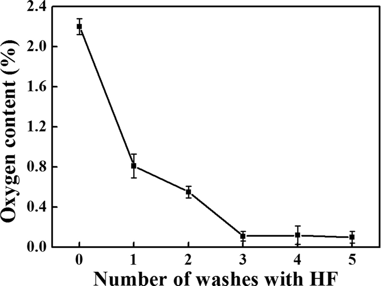
The synthesised SiC was washed using an HF solution to
remove the oxides in the SiC powder, and the variation in the oxygen content
with the number of washing cycles is shown in Fig. 10. Because 5 wt% was
found to be the optimal concentration for removing SiO2,
5 wt% HF solution was used at this stage. We used 40 mL of HF
solution per 0.5 g of SiC powder. Five measurements were performed for
each specimen, and the error was recorded. SiC before washing
contained approximately 2.2% oxygen, which decreased to 0.55%,
0.11%, 0.12%, and 0.1% with the increase in the number of washing cycles. Thus,
the HF solution could remove the oxide impurity during the washing process, and
increasing the number of washing cycles could lower the oxygen content.
Further, the oxygen content rapidly decreased up to three washing cycles.
Beyond this number, it remained almost constant. In addition, beyond three
washing cycles, the standard deviation of the oxygen content increased from
0.05% to 0.09%. Therefore, we believed that washing once and twice could not
sufficiently remove the impurities, depending on the completion of chemical
reaction, and three washing cycles could most efficiently remove the oxide
impurity.
|
Fig. 1 Photographic images of the front and back sides of the poly-Si PV cell before and after etching. |
|
Fig. 2 SEM images of (a) front and (b) back sides of the PV cell with and without etching and EDS mapping results of etched (c) front and (d) back sides. |
|
Fig. 3 SEM images of the poly-Si wafer showing variations in the morphology with milling time. (a) Initial hand-ground Si wafer at (b) 2 h, (c) 4 h, (d) 6 h, (e) 8 h, (f) 10 h, and (g) 20 h. |
|
Fig. 4 FT-IR spectra of the hand-ground and 10 h milled poly-Si wafer. |
|
Fig. 5 Average particle size of the poly-Si wafer according to the milling time. |
|
Fig. 6 Variation in the oxygen content with HF concentration. |
|
Fig. 7 Gibbs free energy as a function of temperature for the SiC generation reactions. |
|
Fig. 8 XRD profiles as a function of synthesis temperature (1200–1400 oC). |
|
Fig. 9 SEM images of the SiC particles synthesised at (a) 1300 oC, (b) 1350 oC, and (c) 1400 oC. |
|
Fig. 10 Variation in the oxygen content of the SiC powder washed with 5 wt% HF solution according to the number of washing cycles. |
|
Table 1 Contents of the main elements of etched poly-Si PV cells as determined by GDMS |
A poly-Si wafer was recovered from a poly-Si PV cell by
acid treatment using a mixed acid composed of HNO3 and HF, which
resulted in the removal of deposited materials such as Ag, Al, and SiNx,
leaving only the Si wafer behind. The content of the removed elements was less
than 0.0000001%, whereas the residual Si content was 99.998594%. The recovered
poly-Si wafer was milled for 20 h using a SPEX mill to prepare 200-nm-size
particles. However, an oxide impurity (SiO2) was produced by the
milling process. This impurity was eliminated by washing the particles with a
5 wt% HF solution, which reduced the oxygen content in the Si powder to
0.01%. The Si powder and carbon black were mixed in 1:1.8 molar ratio, and SiC
was synthesised using SPS performed at a temperature in the range of
1200–1400 oC. The XRD analysis showed that the intensity of Si
and SiC peaks were low, which indicated uncertain crystallinity due to low
crystallisation at 1200 and 1250 oC. At 1300–1400 oC,
only the SiC peak was observed, which indicated the formation of SiC without
any residues. Morphological analysis of the SiC synthesised at
1300–1400 oC showed that the particle size
increased with the increase in the synthesis temperature. Hence, 1300 oC
was considered as a suitable synthesis temperature to synthesise fine SiC
powders. To obtain high-purity SiC, the SiC powder was washed with a 5 wt% HF
solution several times, which led to a steady decrease in the oxygen content of
the powder. After three washing cycles, the oxygen content saturated at 0.11%.
Thus, high-purity SiC can be synthesised using poly-Si wafers recovered from
waste poly-Si PV cells.
This work was supported by the ‘Human Resources Program in
Energy Technology’ of the Korea Institute of Energy
Technology Evaluation and Planning (KETEP) and the
project for ‘New Business R&D Voucher’ between Industry, Academy, and
Research Institute funded by the Korea Ministry of SMEs and Startups in 2019
(Project No. S2718404).
- 1. W.H. Huang, W.J. Shin, L. Wang, W.C. Sun, and M. Tao, Sol. Energy. 144 (2017) 22-31.
-

- 2. Y. Xu, J. Li, Q. Tan, A.L. Peters, and C. Yang, Waste Manag. 75 (2018) 450-458.
-
- 3. Y.S. Zimmermann, C. Niewersch, M. Lenz, Z.Z. Kül, P.F.X. Corvini, and A. Schäffer, T. Wintgens, Environ. Sci.Technol. 48[22] (2014) 13412-13418.
-
- 4. M. Goe, G. Gaustad, Sol. Energy Mater. Sol. Cells. 156 (2016) 27-36.
-
- 5. H. Zhang, W. Ding, K. He, and M. Li, Nanoscale Res. Lett. 5[8] (2010) 1264-1271.
-
- 6. R. Rajarao, R. Ferreira, S.H.F. Sadi, R. Khanna, and V. Sahajwalla, Mater. Lett. 120 (2014) 65-68.
-
- 7. G.M. Kim, G.S. Cho, D.S. Lim, and S.W. Park, J. Ceram. Process. Res. 11[3] (2010) 377-383.
- 8. B.N. Pushpakaran, A.S. Subburaj, S.B. Bayne, and J. Mookken, Renew. Sust. Energy Rev. 55 (2016) 971-989.
-
- 9. F. Lomello, G. Bonnefont, Y. Leconte, N. Herlin-Boime, and G. Fantozzi, J. Eur. Ceram. Soc. 32 (2012) 633–641.
-
- 10. J.H. Kim, C.Y. Kim, and S.C. Choi, J. Korean Ceram. Soc. 55[5] (2018) 440-445.
-
- 11. G.S. An, J.R. Shin, J.U. Hur, A.H. Oh, B.G. Kim, Y.G. Jung, S.C. Choi, J. Alloys Compd. 798 (2019) 360-366.
-
- 12. G.S. An, S.W. Choi, D.H. Chae, H.S. Lee, H.J. Kim, Y.J. Kim, Y.G. Jung, and S.C. Choi, Ceram. Int. 43 (2017) 12888-12892.
-
- 13. G.S. An, D.H. Chae, J.U. Hur, A.H. Oh, H.H. Choi, S.C. Choi, Y.S. Oh, and Y.G. Jung, Ceram. Int. 44 (2018) 2–6.
-
- 14. G.S. An, J.S. Han, J.R. Shin, D.H. Chae, J.U. Hur, H.Y. Park, Y.G. Jung, and S.C. Choi, Ceram. Int. 44 (2018) 12233-12237.
-
- 15. R. Wu, C. Zhang, J. Zhao, and Y. Bai, J. Ceram. Process. Res. 15 (2014) 433-440.
- 16. S. Larpkiattaworn, P. Ngernchuklin, W. Khongwong, N. Pankurddee, and S. Wada, Ceram. Int. 32 (2006) 899-904.
-
- 17. A. Najafi, F.G. Fard, H.R. Rezaie, and N. Ehsani, Powder Technol. 219 (2012) 202-210.
-
- 18. J. Ma, G.Y. Li, Z.Y. Chu, X.D. Li, Y.H. Li, and T.J. Hu, Carbon. 69 (2014) 634-637.
-
- 19. K. Xiang, X. Wang, M. Chen, Y. Shen, H. Shu, and X. Yang, J. Alloys. Compd. 695 (2017) 100-105
-
 This Article
-
2020; 21(4): 400-406
Published on Aug 30, 2020
- 10.36410/jcpr.2020.21.4.400
- Received on Dec 3, 2019
- Revised on Mar 13, 2020
- Accepted on Mar 16, 2020
Services
- Abstract
introduction
experimental procedure
results and discussion
conclusion
- Acknowledgements
- References
- Full Text PDF
Shared
Correspondence to
- Gye Seok An
-
Division of Materials Science and Engineering, Hanyang University, 222 Wangsimni-ro, Seongdong-gu, Seoul 04763, Republic of Korea
Tel : +82-2-2220-0505
Fax: +82-2-2291-6767 - E-mail: faustmaro@hanyang.ac.kr
Clean-Energy Research Institute(CRI), Hanyang University, 222, Wangsimni-ro, Seongdong-gu, Seoul, 04763, Korea
E-mail: jcpr@hanyang.ac.kr