


- Investigation of microstructural and electrical properties of self-aligned Ni-InGaAs alloy contacts to InGaAs as a function of rapid thermal annealing temperature
Shim-Hoon Yuka, Hyun-Gwon Parka, V. Janardhanama, Kyu-Hwan Shima, Sung-Nam Leeb and Chel Jong Choia,*
aSchool of Semiconductor and Chemical Engineering, Semiconductor Physics Research Center (SPRC) Chonbuk National University, Jeonju 561-756, Republic of Korea
bDepartment of Nano-Optical Engineering, Korea Polytechnic University, Siheung 429-793, Republic of Korea
We have investigated
microstructural and electrical properties of self-aligned Ni-InGaAs alloy used
as contact material to InGaAs as a function rapid thermal annealing (RTA)
temperature. The Ni-InGaAs alloy was the only phase resulting from solid-state
reaction between Ni and InGaAs, regardless of the RTA temperature.
Microstructural evolutions of Ni-InGaAs and overlaid Ni films were observed for
increasing RTA temperature. The increase in RTA temperature resulted in
increasing the size of the pinholes formed in the Ni film, which could be
associated with the columnar growth nature of sputter-deposited Ni film. A
relatively uniform Ni-InGaAs layer was formed after RTA at 300 oC,
which could be responsible for the minimum specific contact resistivity
observed at this temperature. Above this temperature, the Ni-InGaAs layer
underwent severe structural degradation such as the formation of microvoids in
its surface area, leading to a rapid increase in specific contact resistivity.
Keywords: InGaAs, Ni, Specific contact resistivity, RTA, Solid-state reaction
InGaAs has attracted much interest as a channel material
for metal-oxide-semiconductor field-effect transistors (MOSFETs) because of its
high electron mobility and light electron effective mass. To realize excellent
performance and highly reliable operation of InGaAs channel MOSFETs, their
source/drain (S/D) contact resistance should be minimized. A general approach
to reduce the S/D contact resistance is by doping the
S/D regions heavily enough that the tunneling of carriers
through S/D contact is possible. Namely, an increase in doping concentration of
S/D regions leads to the significant reduction of S/D contact resistance.
However, because of the low dopant solubility in InGaAs, the typical reduction
of S/D contact resistance through an increase of the doping concentration is
limited [1]. To overcome this problem, a reliable, and low-resistance Ohmic
contact between the S/D and InGaAs is essential [2-4]. There have
been many reports of non-alloyed, Ti-based Ohmic contacts to InGaAs,
with specific contact resistivity of ~ 2 × 10⁻⁷ Ω×cm2
[5-8]. Additionally,
TiW-, Mo-, Pd-, WSi-, and ErAs-based materials have been proposed as alternatives
for contacting InGaAs [9-15].
Similar to self-aligned silicides or germanides, which are
formed by depositing a metal film on Si or Ge and combined with
thermal treatment at elevated temperature, the
metal-InGaAs alloys formed in a self-aligned manner through a
solid-state reaction between a metal and InGaAs are highly required, in
particular for deeply scaled InGaAs-channel MOSFETs
[1, 16]. Among various metals, Ni has been considered as a
viable candidate for self-aligned alloy formation, which is feasible for
providing a low-resistance Ohmic contact to InGaAs for the realization of
ultra-low power devices [17, 18]. At present, considerable efforts have
been made to characterize Ni-InGaAs alloys formed by solid-state reaction
between Ni and InGaAs driven by thermal treatment and demonstrate its potential
use as self-aligned Ohmic contact in devices. Kim et al. [1]
reported for the first time that, in InGaAs MOSFETs fabricated by
forming self-aligned Ni–InGaAs alloy S/D formed at 250 oC and
engineering the Schottky barrier, the S/D resistance was 1/5 lower than in p–n
junction devices. Similarly, it was shown that using self-aligned Ni-InGaAs
contacts, formed by sputtering a Ni film on single-crystalline InGaAs followed
by low-temperature annealing in the 250–400 oC range, was
feasible to realize the n-type MOSFETs with on-/off-state drain current ratio
of ~ 103 [19]. A different study reported that surface
passivation of InGaAs through an InP capping layer or a (NH4)2S
surface treatment reduced the Ni-InGaAs/InGaAs contact resistivity effectively
[20]. Eadi et al. [21] demonstrated that the specific
contact resistivity of Ni-InGaAs/InGaAs was lower in presence of the Tm
interlayer than in its absence. This could be caused by uniform distribution
and pile-up of Si dopant atoms near the Ni-InGaAs/InGaAs interface after
introducing the Tm interlayer. However, most previous works have concentrated
mainly on process techniques to minimize the specific contact resistivity of
Ni-InGaAs/InGaAs contacts for realizing high performance
devices. The dependence of the detailed Ohmic contact on the microstructural
features of the Ni-InGaAs alloy is of great importance for the
successful process integration of self-aligned S/D Ohmic contacts into
InGaAs-based MOSFETs. Nevertheless, the reports on the
relation between electrical and microstructural properties of the Ni-InGaAs/InGaAs
contact formed by solid-state reaction between Ni and InGaAs driven by thermal treatment are limited. In this work, we investigated the microstructural and electrical
properties of self-aligned Ni-InGaAs alloy/InGaAs contact
formed through Ni deposition followed by rapid thermal annealing (RTA)
process as a function of the RTA temperature. In particular, the variation of the Ni-InGaAs/InGaAs specific contact resistivity depending on RTA temperature is directly correlated with the
microstructural evolution of the Ni-InGaAs and overlaid unreactive Ni layers
during the RTA process.
In this study, a 20 nm-thick In0.53Ga0.47As
(InGaAs) epilayer with a doping concentration of 5 ´ 1019 cm3
grown on an InP substrate and an InAlAs buffer layer were used, which was
manufactured by IntelliEPI, Inc. From Hall measurements, the carrier concentration
of InGaAs epilayer was found to be 1.9 × 1019 cm3,
of which value was comparable to that provided by the manufacturer. Prior to Ni
deposition, the sample was chemically cleaned for 10 min in acetone and
methanol and rinsed in de-ionized water to remove contaminants from the surface
of the substrate. Then, the sample was treated with a diluted HF solution to
remove the native oxide. A Ni film with thickness 50 nm was
sputter-deposited on the clean InGaAs epilayer in vacuum, at a pressure of
1 × 10‑6 Torr.
Finally, RTA process was performed at temperatures in the range of
200–400 oC for 1 min under N2 ambient for a
solid-state reaction between Ni and InGaAs. When
considering the limitation of enhancing Ohmic properties
through the increase in the doping concentration associated with the low dopant
solubility in InGaAs, all contacts were formed on InGaAs epilayer with a fixed
doping concentration of 5 × 1019 cm3.
To extract the specific contact resistivity, circular
transmission line method (CTLM) patterns with a constant inner radius of 200 mm
and the inner/outer radius gaps varying from 5 to 50 mm were
defined using standard photolithography. The current–voltage
(I–V) characteristics of the Ni contacts to the InGaAs epilayer were measured
before and after RTA using the precision semiconductor parameter analyzer
(Agilent 4156C). The phase evolution of the samples, driven by the RTA process,
was identified using high-resolution X-ray diffraction (HR-XRD, PANalytical
X’Pert Pro MRD). The microstructures of the samples were characterized by
field-emission transmission electron microscope (FETEM, FEI Tecnai F30). The
surface morphology and root-mean-square (RMS) roughness of the
samples were characterized by field-emission scanning electron
microscopy (FESEM, S4200, Hitachi Ltd.) and atomic force
microscopy (AFM, n-Tracer, NanoFocus Inc.), respectively.
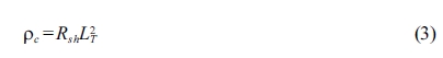
Fig. 1 shows the HR-XRD plots of the Ni contacts to the
InGaAs epilayer as a function of RTA temperatures in the 200–400 oC
range. All samples exhibited the XRD peak with highest diffraction intensity at
63.4°, corresponding to the InP substrate. Since the InGaAs epilayer and InAlAs
buffer layer are lattice-matched to the InP substrate, with the same crystal
structure, their XRD peaks overlap with the strong InP substrate peak [22].
In fact, these could not be sharply separated in XRD spectra
because of very similar XRD peak positions. In addition to the XRD peaks
related to the InP substrate, the characteristic Ni(111) peak was clearly
observed for the as-deposited and 200 oC-annealed
samples. However, for annealing temperatures above 300 oC,
an additional peak corresponding to the Ni-InGaAs formed by solid-state
reaction of Ni and InGaAs was visible. A similar RTA temperature-dependent
phase evolution of the Ni/InGaAs contacts was observed by Kim et al. [1].
They reported that Ni–InGaAs alloy formed after annealing at temperatures
between 250 and 450 oC. Additionally, the presence of the Ni(111)
peak in the samples annealed at 300 and 400 oC indicates that,
in thermal treatments above 300 oC, not the whole deposited Ni
film reacted with the underlying InGaAs epilayer.
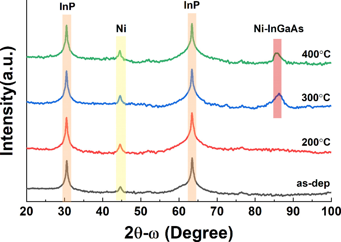
Fig. 2 exhibits the scanning transmission electron
microscopy (STEM) Z-contrast images taken from the Ni contacts to the InGaAs
epilayer treated by RTA in the 200–400 oC temperature range. It
is clear that the columnar growth structure of Ni films, with grain boundaries
oriented perpendicular to the substrate surface irrespective
of the annealing temperature. Such a columnar growth is a typical
feature of sputter-deposited Ni films associated with rotational
mismatch between adjacent Ni grains around the [110] axis [23]. The increase of
the RTA temperature resulted in evolution of the pinholes formed between
columnar Ni grains, i.e., the size of the pinholes increased for
increasing RTA temperatures. As seen in Fig. 2(a) for a sample annealed at
200 oC, a layer with a bright contrast was observed in-between
Ni and the InGaAs epilayer. This layer is believed to be Ni-InGaAs alloy formed
by Ni/InGaAs reaction during the RTA process. The Ni-InGaAs layer
formed after RTA at 200 oC was irregular, with
the thickness of ~ 4 nm. This implies that RTA at 200 oC
is not sufficient to induce solid-state interfacial reaction between the Ni
film and the InGaAs epilayer. However, the presence of the very thin,
non-uniform Ni-InGaAs layer was not detected in the HR-XRD measurements
(Fig. 1). As seen from these, the samples annealed at
300 and 400 oC displayed clearly the Ni-InGaAs layer formed by
Ni/InGaAs reaction driven by RTA process along with the unreacted Ni film. The
RTA process at 300 oC yielded the formation of a Ni-InGaAs
layer with a relatively uniform surface and interface morphology. An unreacted
InGaAs epilayer was found after solid-state reaction between Ni and InGaAs
induced by RTA at 300 oC. On the other hand, this epilayer was
not observed in the sample annealed at 400 oC. In other words,
the InGaAs epilayer was fully consumed by Ni during Ni/InGaAs
reaction at this temperature. There was no further reaction between
Ni and InAlAs, resulting in a very abrupt interface between Ni-InGaAs
and InAlAs. Furthermore, after RTA process at 400 oC,
agglomeration or phase separation of Ni-InGaAs, causing the disintegration of
film continuity, was not observed. However, a structural degradation of the
Ni-InGaAs film was observed, and related to the formation of the microvoids
indicated by arrows in Fig. 2(c). In general, the solid-state reaction between
films involves the process of in/out-diffusion for the formation of
the alloys. It is exactly not clear about the in diffusion
of Ni or the out diffusion of elements in InGaAs for the formation
of the Ni-InGaAs alloy at this moment. However, when considering the formation
of microvoids shown in Fig. 2(c), the massive
out-diffusion of elements consisting of InGaAs might be
predominant for the formation of Ni-InGaAs alloy at higher temperature.
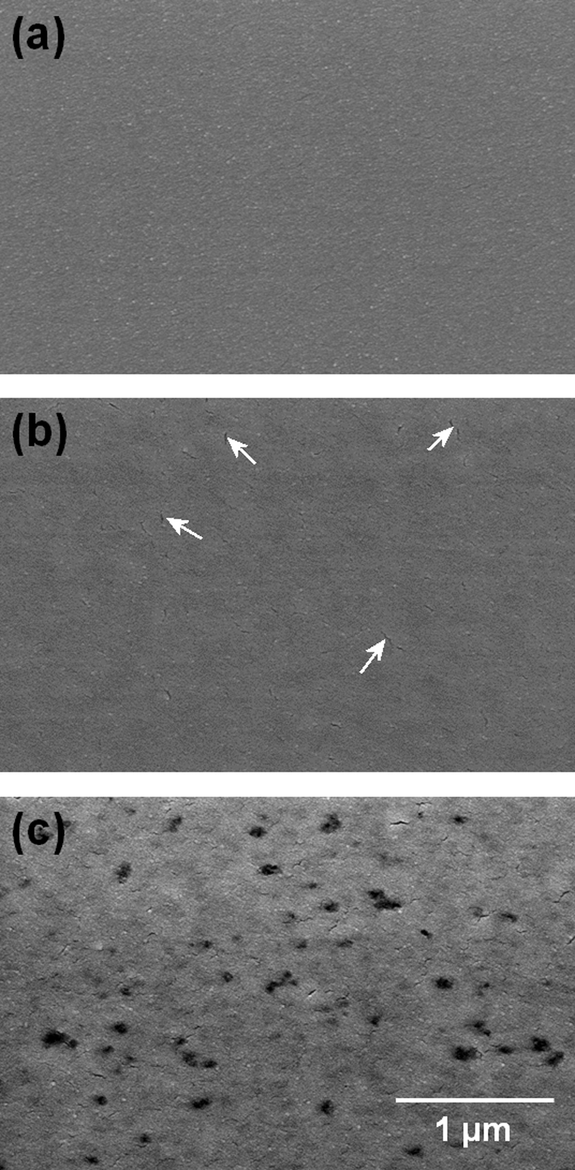
Fig. 3 displays plan-view SEM images of the Ni contacts to
the InGaAs epilayers after annealing at 200, 300, and 400 oC.
The images clearly show an evolution of the surface morphology of Ni
films as the RTA temperature increases. The surface of the sample
annealed at 200 oC was smooth and featureless. The
value of the corresponding RMS roughness, extracted from AFM measurements (not
shown here), was found to be 1.10 nm. In the sample annealed at 300 oC
shown in Fig. 3(b), the surface roughened slightly, displaying the very tiny
pinholes indicated by arrows in the figure, and the RMS roughness increased to
1.29 nm. In the sample annealed at 400 oC, severe morphological
degradation of the surface was observed, as seen from Fig. 3(c). Namely,
numerous large‑scale pinholes were randomly distributed on the surface after
RTA process at 400 oC, which were in
a good agreement with TEM results (Fig. 2).
Additionally, the energy-dispersive X-ray spectroscopy (EDS)
analyses (not shown here) did not reveal differences among the sample.
This could be attributed in part to the presence of unreactive Ni film on
surface shown in Fig. 2 and to the large specimen interaction volume caused by
accelerated electron beam.
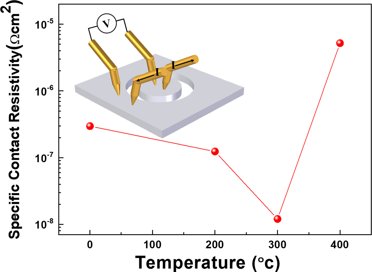
Fig. 4 shows the plot of the specific contact resistivity
of Ni contacts to InGaAs epilayers as a function of RTA temperature. In
particular, four-terminal CTLM measurements were carried out to avoid the
parasitic resistance associated with measurement setup used for measuring the
specific contact resistivity, as shown in the inset of Fig. 4. The specific
contact resistivity was extracted from the CTLM method using following
equations [24]
where, Rsh is the sheet
resistance, C is the correction factor, LT is the effective transfer
length, r is the radius of the inner circle, which was fixed at 200 µm, and s
is the gap space, which was split as 5, 10, 15, 25, 35 and 50 µm. A specific
contact resistivity rc is calculated using Rsh
and LT values determined from a linear fit of RT at the
different gap space values. The specific contact resistivity of
2.97 × 10⁻⁷ W×cm2 was obtained for
the as-deposited sample. The RTA process at 200 oC led
to a slight decrease in specific contact resistivity to 1.23 × 10⁻⁷ W×cm2.
This could be attributed to the formation of the thin Ni-InGaAs layer shown in
Fig. 2(a). In other words, the solid-state reaction between Ni and the InGaAs
epilayer allows the effective removal of the surface damage caused
by the exposure of plasma during sputter-deposition of Ni or
the contamination on surface of the InGaAs epilayer that was unintentionally
introduced during the fabrication process, which can serve as a major cause of
the increase in the specific contact resistivity. A specific contact resistivity
further reduced to 1.02 × 10⁻⁸ W×cm2
was found after RTA at 300 oC. Such a low value could be
associated with the formation of a fairly uniform Ni-InGaAs layer. It should be
noted that the specific contact resistivity obtained after RTA at 300 oC
is lower than those reported for the Ni-InGaAs contact to InGaAs [21, 25, 26].
This implies that Ohmic contact process is feasible for the successful
implementation of high performance InGaAs channel MOSFFETs.
However, a steep increase in the specific contact resistivity
was observed after RTA at 400 oC. As shown by the TEM image of
Fig. 3(c), a Ni-InGaAs layer with uniform interface and surface morphologies
was formed after RTA at 300 oC. Above this temperature, the
morphologies of Ni-InGaAs and of the overlaying unreactive Ni films were significantly
degraded, i.e., the formation of microvoids and pinholes
in the former and the latter, respectively. Namely, the severe structural
degradation of both the Ni-InGaAs and Ni films during RTA at 400 oC
could be the main cause of the large increase in specific contact resistivity.
|
Fig. 1 HR-XRD plots of the Ni contacts to InGaAs epilayers as a function of RTA temperatures in the range of 200–400 oC. |
|
Fig. 2 STEM Z-contrast images of the Ni contacts to InGaAs epilayers treated by RTA at (a) 200 oC, (b) 300 oC, and (c) 400 oC. |
|
Fig. 3 Plan-view SEM images of the Ni contacts to the InGaAs epilayers treated by RTA at (a) 200 oC, (b) 300 oC, and (c) 400 oC. |
|
Fig. 4 Plot of the specific contact resistivity of the Ni contacts to the InGaAs epilayers as a function of RTA temperature. The Inset shows measurement setup used for measuring the specific contact resistivity through four-terminal CTLM measurements. |
Self-aligned Ni-InGaAs Ohmic contacts on an InGaAs
epilayer were formed by sputter-deposition of a Ni film followed by subsequent
RTA process at temperatures in the 200–400 oC range. The
variation of the specific contact resistivity of the Ni-InGaAs contact to
InGaAs caused by RTA process was explained in terms of the microstructural
evolutions of the Ni-InGaAs layer and overlaid unreactive Ni layer. Although an
irregular Ni-InGaAs layer formed after RTA at 200 oC, the
sample annealed at this temperature showed a specific contact resistivity
slightly lower than the as-deposited one. This could be associated with the
curing of plasma damage or unintentional film contamination through the
solid-state reaction between Ni and InGaAs driven by RTA process at 200 oC.
A fairly uniform Ni-InGaAs layer was formed as a result of Ni/InGaAs
solid-state reaction after RTA at 300 oC, which
could be responsible for the minimum specific contact resistivity
measured at this temperature. However, RTA at 400 oC led to the
formation of microvoids on the surface of the Ni-InGaAs layer and the presence
of a sizable number of pinholes in the overlaying unreactive Ni film. Such a
structural degradation could be the main cause of a larger
increase in specific contact resistivity. The results obtained
here demonstrate that the Ni-InGaAs alloy formed by the
self-aligned process could be a promising S/D contact
material for the minimization of specific contact resistivity. Furthermore, the
RTA temperature-dependency of the specific contact resistivity of Ni-InGaAs
contact to InGaAs reported in this work provides a valuable
process guideline for realizing the high performance InGaAs channel MOSFETs.
This study was supported by the National Research Foundation
of Korea (NRF) Grant (NRF-2017R1A2B
2003365) funded by the Ministry of Education, Republic of
Korea, and by Korea Evaluation Institute of Industrial Technology (KEIT) grant
(Project No. 20004314) funded by the
Ministry of Trade, Industry & Energy, Republic of Korea.
- 1. S.H. Kim, M. Yokoyama , N. Taoka , R. Iida , S. Lee, R. Nakane, Y. Urabe, N. Miyata, T. Yasuda, H. Yamada, N. Fukuhara, M. Hata, M. Takenaka, and S. Takagi, Appl. Phys. Exp. 4 (2011) 024201.
-

- 2. S. Takagi, T. Tezuka, T. Irisawa, S. Nakaharai, T. Numata, K. Usuda, N. Sugiyama, M. Shichijo, R. Nakane, and S. Sugahara, Solid-State Electron. 51 (2007) 526-536.
-
- 3. X. Li, R. J. W. Hill, P. Longo, M. C. Holland, H. Zhou, S. Tohms, D. S. Macintyre, and I.G. Thayne, J. Vac. Sci. Technol. B 27 (2009) 3153-3157.
-
- 4. M. Yokoyama, T. Yasuda, H. Takagi, H. Yamada, N. Fukuhara, M. Hata, M. Sugiyama, Y. Nakano, M. Takenaka, and S. Takagi,Dig. Tech. Pap. - Symp. VLSI Technol. (2009) 242-243.
-
- 5. D. Caffin, C. Besombes, J. F. Bresse, P. Legay, G. L. Roux, G. Patriarche, and P. Launay, J. Vac. Sci. Technol. B 15, 854 (1997).
-
- 6. E. Nebauer, M. Mai, E. Richter, and J. Wurfl, J. Electron. Mater. 27, 1372 (1998).
-
- 7. J. Wu, C. Chang, K. Lin, E. Chang, J. Chen, and C. Lee, J. Electron. Mater. 24, 79 (1995).
-
- 8. T. Nittono, H. Ito, O. Nakajima, and T. Ishibashi, Jpn. J. Appl. Phys. 27, 1718 (1988).
-
- 9. A. M. Crook, E. Lind, Z. Griffith, M. J. W. Rodwell, J. D. Zimmerman, A. C. Gossard, and S. R. Bank, Appl. Phys. Lett. 91, 192114 (2007).
-
- 10. A. K. Baraskar, M. A. Wistey, V. Jain, U. Singisetti, G. Burek, B. J. Thibeault, Y. J. Lee, A. C. Gossard, and M. J. W. Rodwell, J. Vac. Sci. Technol. B 27, 2036 (2009).
-
- 11. A. Baraskar, M. A. Wistey, V. Jain, E. Lobisser, U. Singisetti, G. Burek, Y. J. Lee, B. Thibeault, A. Gossard, and M. Rodwell, J. Vac. Sci. Technol. B 28, C5I7 (2010).
-
- 12. A. S. Wakita, N. Moll, S. J. Rosner, and A. Fischer-Colbrie, J. Vac. Sci. Technol. B 13, 2092 (1995).
-
- 13. E. F. Chor, W. K. Chong, and C. H. Heng, J. Appl. Phys. 84, 2977 (1998).
-
- 14. N. Yoshida, Y. Yamamoto, H. Takano, T. Sonoda, S. Takamiya, and S. Mitsui, Jpn. J. Appl. Phys. 33, 3373 (1994).
-
- 15. U. Singisetti, J. D. Zimmerman, M. A. Wistey, J. Cagnon, B. J. Thibeault, M. J. W. Rodwell, A. C. Gossard, S. Stemmer, and S. R. Bank, Appl. Phys. Lett. 94, 083505 (2009).
-
- 16. X. Zhang, H.Guo, X. Gong, Q. Zhou,Y.-R.Lin,H.-Y.Lin, C.-H.Ko, C. H. Wann, and Y.-C. Yeo, Electrochem. Solid-State Lett. 14 (2011) H60-H62.
-
- 17. Ivana, Y.L. Foo, X. Zhang, Q. Zhou, J. Pan, E. Kong, M.H.S. Owen, and Y.-C. Yeo, J. Vacuum Sci. Technol. B 31 (2013) 012202.
-
- 18. P. Shekhter, S. Mehari, D. Ritter, and M. Eizenberg, J. Vacuum Sci. Technol. B 31 (2013) 031205.
-
- 19. X. Zhang, Ivana, H.X. Guo, X. Gong, Q. Zhou, and Y.-C. Yeo, J. Electrochem. Soc. 159 (2012) H511-H515.
-
- 20. M. Abraham, S.-Y. Yu, W. H. Choi, R.T.P. Lee, and S.E. Mohney, J. Appl. Phys. 116 (2014) 164506.
-
- 21. S.B. Eadi, J.C. Lee, H.-S. Song, J. Oh, and H.-D. Lee, Vacuum 166 (2019) 151-154.
-
- 22. S. Mehari, A. Gavrilov, S. Cohen, P. Shekhter, M. Eizenberg, and D. Ritter, Appl. Phys. Lett. 101 (2012) 072103.
-
- 23. J. W. Patten, Thin Solid Films 75 (1981) 205-211
-
- 24. S. B. Eadi, J. C. Lee, H. S. Song, J. O, and H. D. Lee, Vacuum 166 (2019) 151-154
-
- 25. S. Kim, S.K. Kim, S. Shin, J._H. Han, D.M. Geum, J.-P. Shim, S. Lee, H. Kim, G. Ju, J.D. Song, M.A. Alam, H.-J. Kim, J. Electron Devices Soc. 7 (2019) 869-877.
-
- 26. X. Zhang, H.X. Guo, X. Gong, Y.-C. Yeo, ECS J. Solid State Sci. Technol. 1 (2012) P82-P85.
-
 This Article
-
2020; 21(S1): 53-57
Published on May 31, 2020
- 10.36410/jcpr.2020.21.S1.s53
- Received on Dec 17, 2019
- Revised on Mar 24, 2020
- Accepted on Apr 2, 2020
Services
- Abstract
introduction
experimental details
results and discussion
conclusions
- Acknowledgements
- References
- Full Text PDF
Shared
Correspondence to
- Chel Jong Choi
-
School of Semiconductor and Chemical Engineering, Semiconductor Physics Research Center (SPRC) Chonbuk National University, Jeonju 561-756, Republic of Korea
Tel : +82-63-270-3365
Fax: +82-63-270-3585 - E-mail: cjchoi@jbnu.ac.kr
Clean-Energy Research Institute(CRI), Hanyang University, 222, Wangsimni-ro, Seongdong-gu, Seoul, 04763, Korea
E-mail: jcpr@hanyang.ac.kr