


- Effect of gas condition on graphene synthesized by rapid thermal chemical vapor deposition
Yang Soo Leea,†, Dong In Jeonga,†, Yeojoon Yoonb,†, Byeongmin Baekc, Hyung Wook Choid, Seok Bin Kwona, Do Hun Kimc, Young Joon Honge, Won Kyu Parkf, Young Hyun Songg, Bong Kyun Kangc, Dae Ho Yoona,* and Woo Seok Yangc,*
aSchool of Advanced Materials Science and Engineering, Sungkyunkwan University, Suwon 440-746, Republic of Korea
bDepartment of Environmental Engineering, Yonsei University, Wonju-si, Gangwon-do, Republic of Korea
cNano Materials and Components Research Center, Korea Electronics Technology Institute, Seongnam-si, Gyeonggi-do 13509, Republic of Korea
dSKKU Advanced Institute of Nanotechnology (SAINT), Sungkyunkwan University, Suwon 16419, Korea
eDepartment of Nanotechnology and Advanced Material Engineering, Sejong University, Seoul 05006, Republic of Korea
fNano Material Division, Cheorwon Plasma Research Institute, Cheorwon, Gangwon, 24047, Republic of Korea
gLighting Design & Component Research Center, Korea Photonics Technology Institute, Gwangju 61007, Republic of Korea
Graphene was synthesized using
rapid thermal chemical vapor deposition (RT-CVD) equipment designed to produce
large-area graphene at high speed. The effects of methane (CH4),
argon (Ar), and hydrogen (H2) gases were investigated between 800 oC
and 1,000 oC during heating and cooling in the graphene
synthesis process. The findings reveal that multilayer domains increased due to
hydrogen pretreatment with increase in temperature. Furthermore, when
pretreated with the same gas, it was confirmed that the post-argon-treated
sample cooled from 1,000 oC to 800 oC had a
higher ID/IG value than that of the other samples. This
result was consistent with the sheet resistance properties of graphene. The
sample prepared in methane atmosphere maintained during both the pre-treatment
and post-treatment demonstrated the lowest sheet resistance of 787.49 Ω/sq. Maintaining the methane gas atmosphere in the
high-temperature region during graphene synthesis by RT-CVD reduced the defects
and improved the electrical property.
Keywords: Graphene, Rapid thermal chemical vapor deposition, Gas condition
The progress in information and communication technology
has led to the rapid development of electronic materials
industry [1]. With the growing popularity of smart devices, research on high
performance and light- weight
products has rapidly increased in the last several years.
Carbon materials (carbon nanotube, graphene, g–C3N4) have
attracted tremendous attention as high value-added materials due to their
lightweight, higher strength, good chemical, and thermal stability
properties compared to other materials [2, 3]. In addition, its
excellent electrical properties and chemical stability
makes a potential candidate for energy storage, batteries and
electrode materials [4-6].
Especially, graphene, sp2-hybridized carbon
atoms, has superior electronic, optical, thermal, and mechanical
properties [7, 8].
To effectively apply the various excellent properties of
graphene to electronic materials, it is necessary to study the conditions of
graphene synthesis process [9]. Chemical vapor deposition (CVD) is a suitable
method for producing large-scale single-layer graphene [10, 11]. Graphene
synthesized by CVD is a polycrystalline material, in which several
micrometer-scale domains consisting of carbon, grow in two dimensions. Also,
CVD method has been conducted to achieve uniform growth of single and large
area carbon films on the transition metal surface at relatively low process
costs [11-13]. During CVD synthesis of graphene, the synthetic
conditions such as gas used, temperature, and pressure, affect the characteristics
of the graphene synthesized. Therefore, investigating the synthesis mechanism
of large-area and high-quality graphene is necessary to effectively apply the
excellent properties of graphene to transparent electrodes and various
electronic devices [5, 14].
However, thin film synthesis in conventional thermal CVD
(T-CVD) equipment is time consuming, hindering the
commercialization of monolayer graphene. Thus, the rapid thermal chemical vapor
deposition (RT-CVD, RHP400V, NPS Corporation) equipment is suitable for
graphene synthesis on the surfaces of large-area metal catalysts [15].
Furthermore, the RT-CVD could synthe-
size the graphene film about 7 times faster than the conventional T-CVD
equipment [15]. Since the RT-CVD equipment is not widely available, there have
been limited studies on the suitable process conditions for high-speed graphene
synthesis. To investigate the properties of synthesized graphene using the
RT-CVD, have been analyzed such as the crystal structure, defects,
optical properties, and electrical properties [16, 17].
Process conditions such as temperature, gas, and pressure
affect the properties of chemical-vapor-deposition materials
[18-20]. The optimum ratio of hydrocarbon gas to hydrogen gas promotes the
synthesis of low-defect monolayer graphene on copper foils, which was
determined by the interaction between graphene growth and etching [21].
Especially, hydrogen plays an important role in the growth process of graphene
by CVD as an activator for size-limited graphene domain growth and carbon
adsorption on the surface of copper foils [21, 22]. Furthermore, the synthesis
of graphene using a high purity methane precursor was reported at 800 oC,
which is lower than the typical temperature for graphene synthesis [23].
In this study, the graphene was synthesized in various gas
conditions and growth temperatures (800 oC ~ 1,000 oC)
by RT-CVD. In addition, to understand the effect of methane (hydrocarbon
precursor), hydrogen, and argon (inert gas) on graphene synthesized by RT-CVD process,
the synthetic processes were divided into 5 steps. The characteristics of
graphene on various growth conditions was investigated.
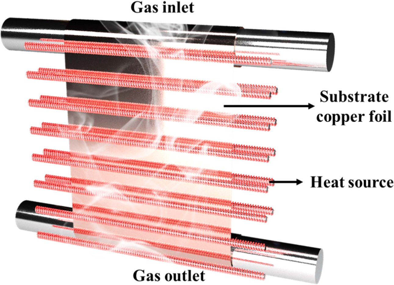
Graphene synthesis was performed using a RT-CVD system
(RHP400V, NPS Corporation). Fig. 1 show the schematic of RT-CVD furnace. Since
the RT-CVD system is equipped with several linear heating elements,
it can heat up to over 7 times faster than a typical CVD furnace. Graphene was
grown on the surface of a rolled copper foil (Nippon Mining & Metals
Corporation, at least 99.9%) having a thickness of 0.035 mm, width of 350 mm,
and length of 480 mm.
Within the CVD equipment, the carbon precursor was
adsorbed on both sides of the copper foil. To obtain monolayer
graphene, the graphene grown on one side of the copper foil was etched with
oxygen plasma for 10 s at a pressure of 110 mTorr and with 50 W RF
power using reactive ion etching equipment (SciEnTech Co., Ltd.).
To prevent the tearing of graphene after the etching of the copper foil,
polymethyl methacrylate (PMMA) was spin coated on the graphene with a spin
coater at 4,000 rpm for 30 s. The PMMA coated graphene/Cu sample was thermally
cured at 180 oC for 1 min using a hot plate. A silicon wafer
coated with a 300-nm-thick oxide layer was sonicated in Standard Cleaning-1
(SC-1) solution (NH4OH:H2O2:H2O = 1:1:5). The
PMMA-coated thermally cured graphene/Cu samples were then
etched with ammonium persulfate (APS) solution for 8 h. The APS solution was
prepared by dissolving 32 g of APS powder in 2 L of deionized water. The
PMMA-coated graphene film was washed with DI water and transferred to the SiO2/Si
wafer. Finally, the PMMA was removed with acetone for about 3 h.
|
Fig. 1 Schematic of RT-CVD furnace capable of synthesizing large-area graphene faster. |
The morphology of the synthesized graphene was measured
using a field emission scanning electron microscope (FE-SEM, JSM-700F, JEOL).
High purity (99.999%) commercial argon, hydrogen (MS DONGMIN SPECIALTY
GAS Ltd.), and methane (KOREA NOBLE GAS CO.) gas were used. The
absorbance spectrum of graphene was measured using a UV-visible spectro- photometer (Cary 60 UV-Vis, Agilent
Technologies). The electronic structure of graphene was evaluated using a Raman
spectroscopy (Confotec MR520, SOL instruments) with a 532 nm laser source, and
the electrical properties of graphene were measured using a four-point probe
instrument (Loresta-GP/MCP-T610, Mitsubishi Chemical Analytech Co.).
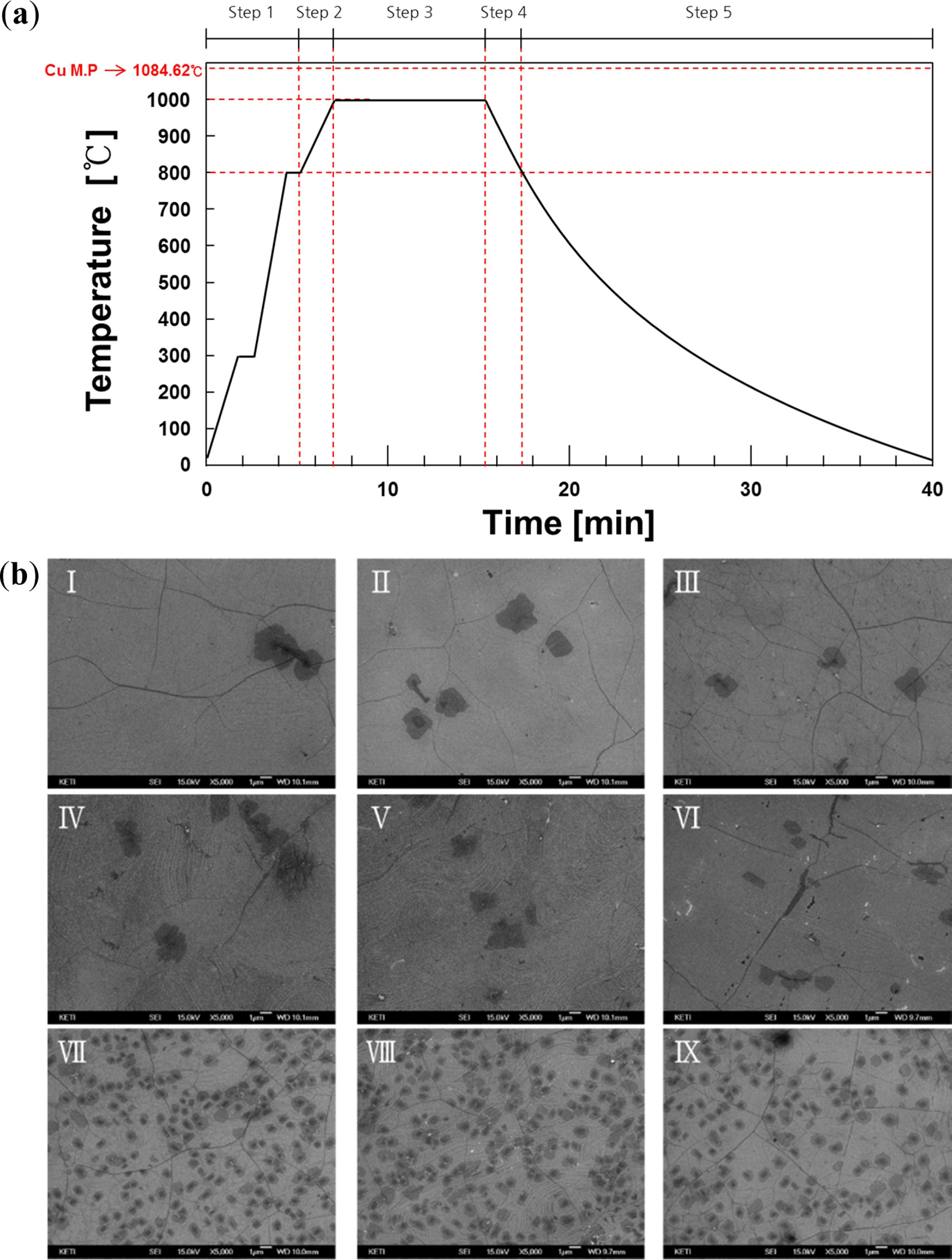
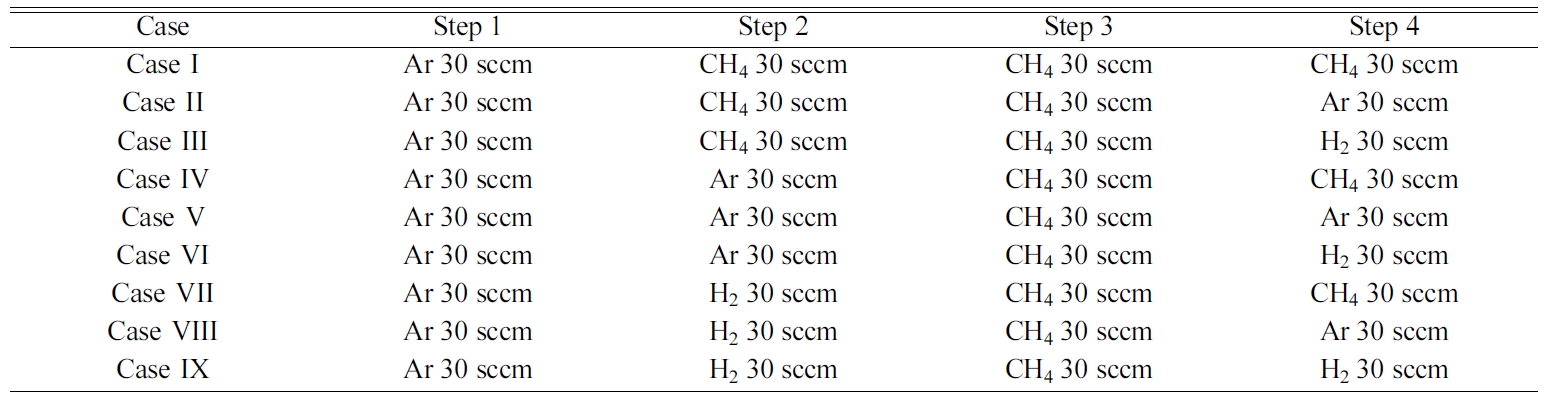
The synthesis process was separated into 5 steps to analyze
the impact of the different gas species on graphene properties at 800 oC
and 1,000 oC. In all the graphene synthesis processes, the
RT-CVD chamber was evacuated and maintained to 550 mTorr using a rotary vacuum
pump.
At the beginning of the process (Table. 1), It was heat up
to 800 oC from room temperature, at a heating rate of 140 oC/min
in an atmosphere of 30 sccm Ar flowing (Step1). Next, the copper foil was
thermally treated from 800 oC to 1,000 oC under
CH4, Ar, and H2 gases at an atmosphere of 30 sccm gas
flowing (Step2). Graphene was synthesized at 1,000 oC for 500
seconds in an atmosphere of 30 sccm CH4 flowing (Step3). After
the completion of graphene growth, an atmosphere of 30 sccm
of CH4, Ar, and H2 gases were flowed while lowering the
temperature of the copper foil from 1,000 oC to 800 oC
(Step4). Finally, the CVD chamber was cooled from 800 oC to
room temperature with continuous N2 flow at the rate of 1,0000 sccm.
Fig. 2(a) shows the temperature conditions of the RT-CVD synthesis process. The
gas conditions were as follows: Sample I: CH4 (step2)-CH4
(step4) flow, Sample II: CH4-Ar, Sample III: CH4-H2,
Sample IV: Ar-CH4, Sample V: Ar-Ar, Sample VI: Ar-H2,
Sample VII: H2-CH4, Sample VIII: H2-Ar, and
Sample IX: H2-H2, respectively. The FE-SEM surface images
of graphene transferred onto the silicon wafer were as shown in Fig. 2(b). The
FE-SEM images of samples VII, VIII, and IX show the
formation of numerous multilayer graphene domains when
hydrogen gas was introduced in Step2. Graphene was synthesized by
methane and the remaining hydrogen
promoted the formation of multilayer graphene on the
surface of the transition metal catalyst in Step3 [21].
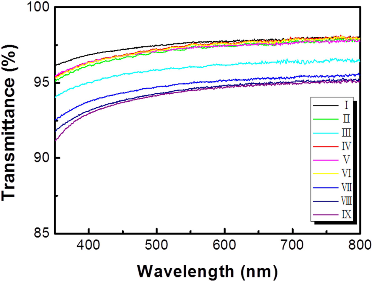
The optical properties of the synthesized graphene are
shown in Fig. 3. For samples VII, VIII, and IX, in which
multilayer domains were formed due to hydrogen
pretreatment, the measured transmittances were 94.97, 94.60, and
94.48%, respectively, and indicated an average absorption
rate of 5.32% (at 550 nm). In contrast, sample I exhibited the best transparency
(97.64%). Graphene was found to absorb approximately 2.3% of incident white
light [24, 25]. It was concluded that the graphene
domain islands with about 2~3 layers decreased the light
transmittance. Due to the effects of residual hydrogen and
methane on fast process rates, the domain density can
be increased. Lower nucleation barriers can increase graphene nucleation
density on the copper oxide compared with that ramped up and annealed on gas
conditions without hydrogen [21].
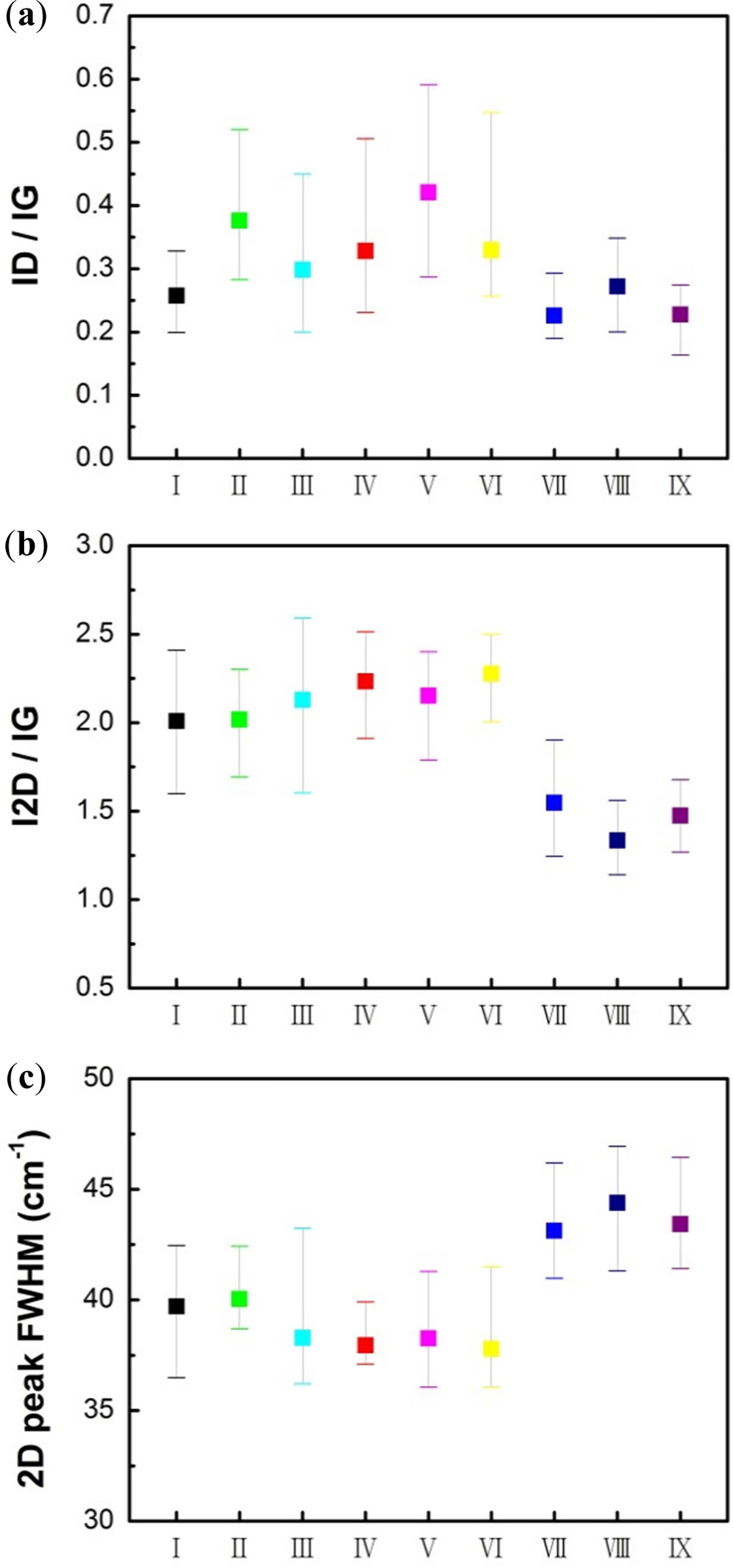
The statistical analyses of Raman spectral data of
graphene grown in nine different gas conditions were as presented in Fig. 4.
Raman spectroscopy can provide information about the lattice structure of the
target material using single frequency light such as a laser. The main features
in the Raman spectra of carbon were the D peaks (1,350 cm-1),
G peaks (1,580 cm-1)
and 2D peaks (2,700 cm-1),
respectively. The disorder-induced D peak is not apparent in pristine graphene
because of crystal symmetry, while the G peak, which is the primary in-plane
vibrational mode according to the bond stretching in both
rings and chains, was derived from all pairs of sp2-hybridized
carbon atoms. One way to characterize the disorder and defect levels of
graphene is to use Raman spectra for the intensity ratio (ID/IG)
of the D peak to G peak. Furthermore, the 2D peak is owing to double
resonance, which links the phonon wave vectors to the
electronic band structure. In addition, near the K point containing the phonon,
the 2D peak occurs as a result of the 2-phonon resonance process. The 2D peak
is very prominent in graphene than in bulk graphite.
Graphene can be deduced from the number of layers of
graphene using the intensity ratio of 2D peak to G peak (I2D/IG).
The I2D/IG ratio of pristine single-layer graphene was
3.4 [25-31]. In this study, Raman ratio was directly obtained from the
statistical analysis with 20 points. The ID/IG ratios of
samples I (0.258), VII (0.226), VIII (0.272), and IX (0.228) were lower than
that of the other samples. Formation of multi-layer graphene domains with
hydrogen pretreatment, and low ID/IG ratios were
calculated for samples VII, VIII, and IX. Among the samples synthesized under
the same gas conditions in Step2, the strongest D peak appeared for
the sample for which argon was introduced in Step4.
The absence of a reducing gas such as hydrogen and methane
to protect from oxidizing impurities promote defects [31].
The average value of I2D/IG ratio of
graphene and the full width at half maximum (FWHM) of the 2D peak distinguished
the graphene layer [27]. Samples VII, VIII, and IX exhibited lower I2D/IG
ratios and higher FWHM values than those of the samples prepared in
other conditions.
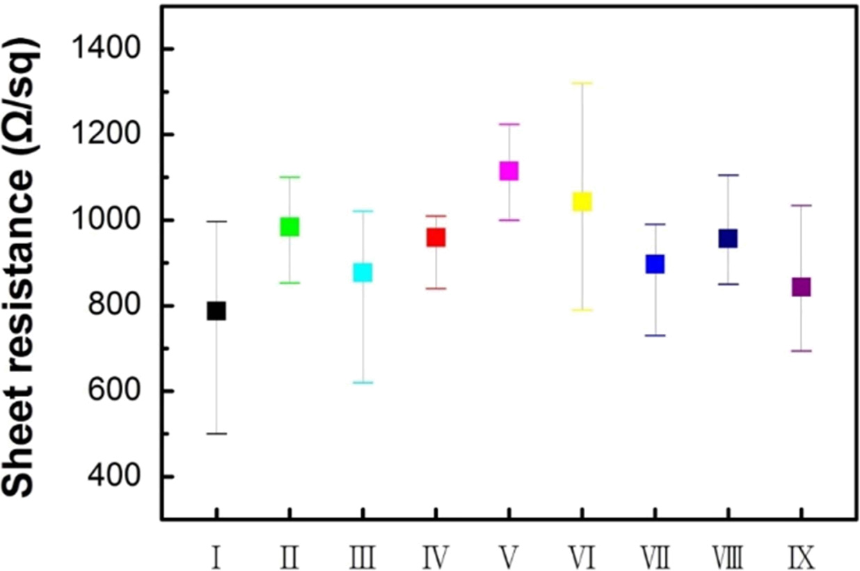
Fig. 5 shows the graphene sheet resistance to nine
graphene synthesis gas conditions. The lowest average sheet resistance of
787.49 Ω/sq was measured for sample 1. Among the samples
synthesized under the same gas conditions in Step2, the highest
sheet resistance was recorded for the sample for which argon was introduced in
Step4. The trend of sheet resistance (Fig. 5) is similar to that of ID/IG
ratio (Fig. 4 (a)). Further, the relatively poor electrical conductivity of
graphene is due to structural defects formed during the synthesis process [10].
Table 1
|
Fig. 2 (a) Process steps of graphene synthesis using RT-CVD. And (b) FE-SEM images of graphene synthesized in nine different gas conditions; Sample I: CH4-CH4, Sample II: CH4-Ar, Sample III: CH4-H2, Sample IV: Ar-CH4, Sample V: Ar-Ar, Sample VI: Ar-H2, Sample VII: H2-CH4, Sample VIII: H2-Ar, Sample IX: H2-H2. |
|
Fig. 3 Optical transmittance of graphene synthesized in nine different gas conditions. |
|
Fig. 4 Raman spectral data of graphene synthesized in nine different gas conditions. (a) ID/IG ratio, (b) I2D/IG ratio, and (c) 2D peak FWHM. |
|
Fig. 5 Sheet resistance of graphene synthesized in nine different gas conditions. |
Graphene synthesis using RT-CVD under various gas
conditions and hydrogen pre-treatment in Step2 led to the growth of multi-layer
graphene domains. On the other hand, the absence of a reducing gas promoted
defects, which led to the degradation of electrical characteristics.
The flow of methane in Step2 and Step4 during graphene synthesis by
RT-CVD caused less degradation of electrical properties and provided
optical properties similar to that of pristine graphene.
This work was supported by the “World Class 300 Project
(R&D) (S2561932)” of the MOTIE, MSS (Korea). This work
was supported by the Ministry of Trade, Industry and Energy through Technology
Innovation Program (Grant No. 10067449). This work was partly supported
by the GRRC program of Gyeonggi province [GRRC
Sungkyunkwan 2017-B03, Development of chemical sensor based on metal oxide
materials]. This work was supported by the Korea Basic Science
Institute (KBSI) National Research Facilities
& Equipment Center (NFEC) grant
funded by the Korea government (Ministry of
Education) (No. 2019R1A6C1010031).
†Y.S. Lee, †D.I.
Jeong, and †Y. Yoon contributed equally to
this work. †Y.S. Lee, †D.I. Jeong, and †Y.
Yoon designed and wrote this study.
- 1. K.S. Novoselov, V. Fal, L. Colombo, P. Gellert, M. Schwab, and K. Kim, Nature 490[7419] (2012) 192-200.
-

- 2. O.C. Compton and S.T. Nguyen, Small 6[6] (2010) 711-723.
-
- 3. C. Lee, X. Wei, J.W. Kysar, and J. Hone, Science 321[5887] (2008) 385-388.
-
- 4. M. Pumera, Energy Environ. Sci. 4[3] (2011) 668-674.
-
- 5. X. Wang, L. Zhi, and K. Müllen, Nano Lett. 8[1] (2008) 323-327.
-
- 6. X. Yang, J. Zhu, L. Qiu, and D. Li, Adv. Mater. 23[25] (2011) 2833-2838.
-
- 7. V. Goyal and A.A. Balandin, Appl. Phys. Lett. 100[7] (2012) 073113.
-
- 8. M.I. Katsnelson, Mater. Today 10[1-2] (2007) 20-27.
-
- 9. A.C. Neto, F. Guinea, N.M. Peres, K.S. Novoselov, and A.K. Geim, Rev. Mod. Phys. 81[1] (2009) 109-162.
-
- 10. K.S. Kim, Y. Zhao, H. Jang, S.Y. Lee, J.M. Kim, K.S. Kim, J.-H. Ahn, P. Kim, J.-Y. Choi, and B.H. Hong, Nature 457[7230] (2009) 706-710.
-
- 11. A. Reina, X. Jia, J. Ho, D. Nezich, H. Son, V. Bulovic, M.S. Dresselhaus, and J. Kong, Nano Lett. 9[1] (2008) 30-35.
-
- 12. M. Losurdo, M.M. Giangregorio, P. Capezzuto, and G. Bruno, Phys. Chem. Chem. Phys., 13[46] (2011) 20836-20843.
-
- 13. C. Mattevi, H. Kim, and M. Chhowalla, J. Mater. Chem. 21[10] (2011) 3324-3334.
-
- 14. X. Li, Y. Zhu, W. Cai, M. Borysiak, B. Han, D. Chen, R.D. Piner, L. Colombo, and R.S. Ruoff, Nano Lett. 9[12] (2009) 4359-4363.
-
- 15. J. Ryu, Y. Kim, D. Won, N. Kim, J.S. Park, E.-K. Lee, D. Cho, S.-P. Cho, S.J. Kim, and G.H. Ryu, ACS Nano 8[1] (2014) 950-956.
-
- 16. F. Banhart, J. Kotakoski, and A.V. Krasheninnikov, ACS Nano 5[1] (2010) 26-41.
-
- 17. A. Hashimoto, K. Suenaga, A. Gloter, K. Urita, and S. Iijima, Nature 430[7002] (2004) 870-873.
-
- 18. S. Bhaviripudi, X. Jia, M.S. Dresselhaus, and J. Kong, Nano Lett. 10[10] (2010) 4128-4133.
-
- 19. Y. Hao, M. Bharathi, L. Wang, Y. Liu, H. Chen, S. Nie, X. Wang, H. Chou, C. Tan, B. Fallahazad, H. Ramanarayan, C. W. Magnuson, E. Tutuc, B. I. Yakobson, K. F. McCarty, Y.-W. Zhang, P. Kim, J. Hone, L. Colombo, and R. S. Ruoff, Science 342[6159] (2013) 720-723.
-
- 20. X. Li, W. Cai, J. An, S. Kim, J. Nah, D. Yang, R. Piner, A. Velamakanni, I. Jung, E. Tutuc, E. Tutuc, S. K. Banerjee, L. Colombo, and R. S. Ruoff, Science 324[5932] (2009) 1312-1314.
-
- 21. I. Vlassiouk, M. Regmi, P. Fulvio, S. Dai, P. Datskos, G. Eres, and S. Smirnov, ACS Nano 5[7] (2011) 6069-6076.
-
- 22. X. Li, C.W. Magnuson, A. Venugopal, R.M. Tromp, J.B. Hannon, E.M. Vogel, L. Colombo, and R.S. Ruoff, J. Am. Chem. Soc. 133[9] (2011) 2816-2819.
-
- 23. L. Tao, J. Lee, H. Chou, M. Holt, R.S. Ruoff, and D. Akinwande, ACS Nano 6[3] (2012) 2319-2325.
-
- 24. R.R. Nair, P. Blake, A.N. Grigorenko, K.S. Novoselov, T.J. Booth, T. Stauber, N.M. Peres, and A.K. Geim, Science 320[5881] (2008) 1308-1308.
-
- 25. D. Yoon, Y.-W. Son, and H. Cheong, Phys. Rev. Lett. 106[15] (2011) 155502.
-
- 26. Z. Ni, Y. Wang, T. Yu, and Z. Shen, Nano Res. 1[4] (2008) 273-291.
-
- 27. Y. Hao, Y. Wang, L. Wang, Z. Ni, Z. Wang, R. Wang, C.K. Koo, Z. Shen, and J.T. Thong, Small 6[2] (2010) 195-200.
-
- 28. D.R. Cooper, B. D’Anjou, N. Ghattamaneni, B. Harack, M. Hilke, A. Horth, N. Majlis, M. Massicotte, L. Vandsburger, and E. Whiteway, ISRN Condens. Matter Phys. 2012 (2012) 1-56.
-
- 29. I. Childres, L.A. Jauregui, J. Tian, W. Park, H. Cao, and Y.P. Chen, New Developments in Photon and Materials Research 1. 13[2] (2013) 025008.
-
- 30. C. Casiraghi, S. Pisana, K. Novoselov, A. Geim, and A. Ferrari, Appl. Phys. Lett. 91[23] (2007) 233108.
-
- 31. S. Choubak, P.L. Levesque, E. Gaufres, M. Biron, P. Desjardins, and R. Martel, J. Phys. Chem. C 118[37] (2014) 21532-21540.
-
 This Article
-
2020; 21(S1): 47-52
Published on May 31, 2020
- 10.36410/jcpr.2020.21.S1.s47
- Received on Dec 16, 2019
- Revised on Apr 21, 2020
- Accepted on May 4, 2020
Services
- Abstract
introduction
experimental
characterization
results and discussion
conclusion
- Acknowledgements
- References
- Full Text PDF
Shared
Correspondence to
- Dae Ho Yoon a and Woo Seok Yang c
-
aSchool of Advanced Materials Science and Engineering, Sungkyunkwan University, Suwon 440-746, Republic of Korea
cNano Materials and Components Research Center, Korea Electronics Technology Institute, Seongnam-si, Gyeonggi-do 13509, Republic of Korea
Tel./Fax: +82-31-290-7388 (D. Yoon), +82-31-789-7057 (W. Yang)
E - E-mail: dhyoon@skku.edu, wsyang@keti.re.kr
Clean-Energy Research Institute(CRI), Hanyang University, 222, Wangsimni-ro, Seongdong-gu, Seoul, 04763, Korea
E-mail: jcpr@hanyang.ac.kr