


- Enhanced optical output power of AlGaN/GaN ultraviolet light-emitting diodes fabricated with breakdown induced conductive channels
Seonghoon Jeonga, Sung-Nam Leeb, Chel-Jong Choia,* and Hyunsoo Kima,*
aSchool of Semiconductor and Chemical Engineering, Semiconductor Physics Research Center, Jeonbuk National University, Jeonju 54896, Korea
bDepartment of Nano-Optical Engineering, Korea Polytechnic University, Siheung 15073, Korea
The enhanced optical output
power of AlGaN/GaN deep ultraviolet light-emitting diodes (UV LEDs) were
demonstrated by using the breakdown-induced conductive channels (BICCs). The
BICCs could be made by electrical reverse biasing between two adjacent contact
pads formed on top p-type layers with a certain distance, causing an electrical
breakdown of pn junction and hence a generation of conductive channels.
Accordingly, the reflective Ni/Ag/Pt electrodes could be formed simultaneously
on the top p-type layer and the other p-type layer with the BICCs, acting as
the p- and n-contacts, respectively. The deep UV LEDs fabricated with the BICCs
produced the enhanced optical output power by 15% as compared to the reference
LEDs, which were fabricated with the conventional Ti/Al/Ti/Au layers formed on
mesa-etched n-type layer. This could be due to the reduced light absorption at
the n-contact pads, indicating that the use of BICCs will be very suitable for
obtaining better output performance of deep UV emitters.
Keywords: Ultraviolet, Light emitting diodes, Breakdown-induced conductive channels, AlGaN/GaN
GaN-based light-emitting diodes (LEDs) are being widely
used in a variety of applications such as displays, mobile
communications, automotive lighting and interior/exterior
lighting [1-3]. Recently, the deep ultraviolet light-emitting diodes (UV LEDs)
fabricated with the AlGaN/GaN-based materials have drawn considerable attention
owing to their potential applications with an extremely short emission
wavelength of ~260 nm such as sterilization, medical treatment, purification,
and bioindustry [4-7]. However, for faster commercialization,
it is still necessary to improve the external quantum efficiency or to increase
the optical output power of UV LEDs [1-7].
According to the literatures [8-14], the deep UV LEDs
were found to suffer from very poor light extraction efficiency. This was due
to the strong light absorption through the top p-GaN contact layer
[8-10], the anisotropic optical polarization nature of AlGaN-based
materials [8, 11, 12], and a significant total internal reflection
occurring as a result of a large difference in the refractive indices between
AlGaN-based semiconductors and substrate or air [8], [13-14].
Therefore, because the light experiences multiple internal reflections within a
chip, it is quite crucial to suppress the absorption of trapped light by
avoiding highly absorptive materials such as electrodes. The conventional metal
electrodes used in the deep UV LEDs are Ag- and Ti/Al-based schemes as a
reflective p-contact and a n-contact, respectively, because they are very
suitable for the formation of Ohmic contact upon thermal annealing. However,
the thermally annealed Ti/Al-based n-contacts are
generally known to have lower optical reflectivity against the Ag.
Very recently, our group showed that the reverse breakdown
mechanism of GaN-based LED, namely, the defect-assisted Zener breakdown. More
specifically, the reverse biasing of GaN p-n junction wan shown to induce a
local breakdown through the native crystal defects such as V-pits.
Interestingly, this phenomenon resulted in a formation of conductive channels,
which is so-called the breakdown-induced conductive channels
(BICCs). By using BICCs, AC-controllable light-emitting devices without any
AC–DC converter [15] or the flat-type InGaN-based LEDs without an n-contact
electrode [16] could be demonstrated.
In this study, based on the BICCs method, we attempted to
use the reflective Ni/Ag/Pt contact as the p- and n-electrodes for AlGaN/GaN deep
UV LEDs simultaneously. By using the BICCs, the Ni/Ag/Pt contact could be
served as the n-type electrodes as well as p-electrodes. The deep UV LEDs
fabricated with the BICCs produced the enhanced optical output power by 15% as
compared to the reference LEDs. This could be attributed to the reduced light
absorption at the n-contact by 65%. These results indicate that the use of
BICCs will be very suitable for obtaining better output performance
of deep UV emitters as well as for reducing the process
step of metal deposition.
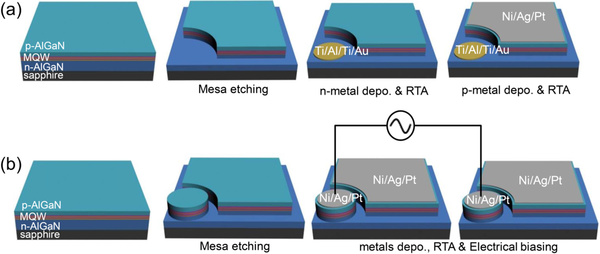
To fabricate the deep UV LEDs, commercially available
AlGaN/GaN wafers (the peak emission wavelength of 273 nm) grown on c-plane
sapphire substrate by metalorganic chemical vapor deposition were
used. The structure of UV LEDs consisted of n-type AlGaN cladding layer, five
periods of AlGaN/AlGaN multiple quantum wells, p-type AlGaN cladding
layer, and a p-type GaN contact layer. Fig. 1(a) shows the schematic
fabrication procedure of reference UV LEDs. For device fabrication, the mesa was defined
by conventional photolithography and dry
etching by inductively coupled plasma
reactive ion etching system. The etching depth was about 400 nm. As the
n-electrode, the 20/60/20/100
nm-thick Ti/Al/Ti/Au layers were then e-beam evaporated on the exposed n-AlGaN
layer, followed by rapid thermal annealing (RTA) at 950 oC for
1min in N2. As the p-electrodes, 2/200/30 nm-thick Ni/Ag/Pt layers
were deposited on p-AlGaN, followed by RTA at 550 oC for 1 min
in air. In addition, the schematic fabrication procedure of UV LEDs having
BICCs (referred hereto as ‘BICCs-LEDs’) is shown in Fig. 1(b). First, the mesa
was also defined by dry etching, while it should be noted that the small
circular mesa was additionally defined at the expected position of n-electrodes. Then, the Ni/Ag/Pt layers were
deposited on the top of each mesa simultaneously, followed by
RTA at 550 oC for 1 min in air. To generate the BICCs, the alternating electrical biasing
(± 15 V with a compliance current of 40 mA) was performed between
two adjacent contact pads, in which the electrical junction breakdown occurs.
To investigate the contact properties, transmission line model (TLM) patterns
were also formed on the same wafer [17], in which the same method to generate
BICCs was carried out. The electrical and optical characteristics of the
fabricated devices were measured using a probestation system with parameter
analyzer (HP4156A), photodiode (883-UV),
and optical spectrometer (Ocean Optics USB2000).
|
Fig. 1 Schematic fabrication procedures for (a) reference LEDs and (b) BICCs-LEDs. |
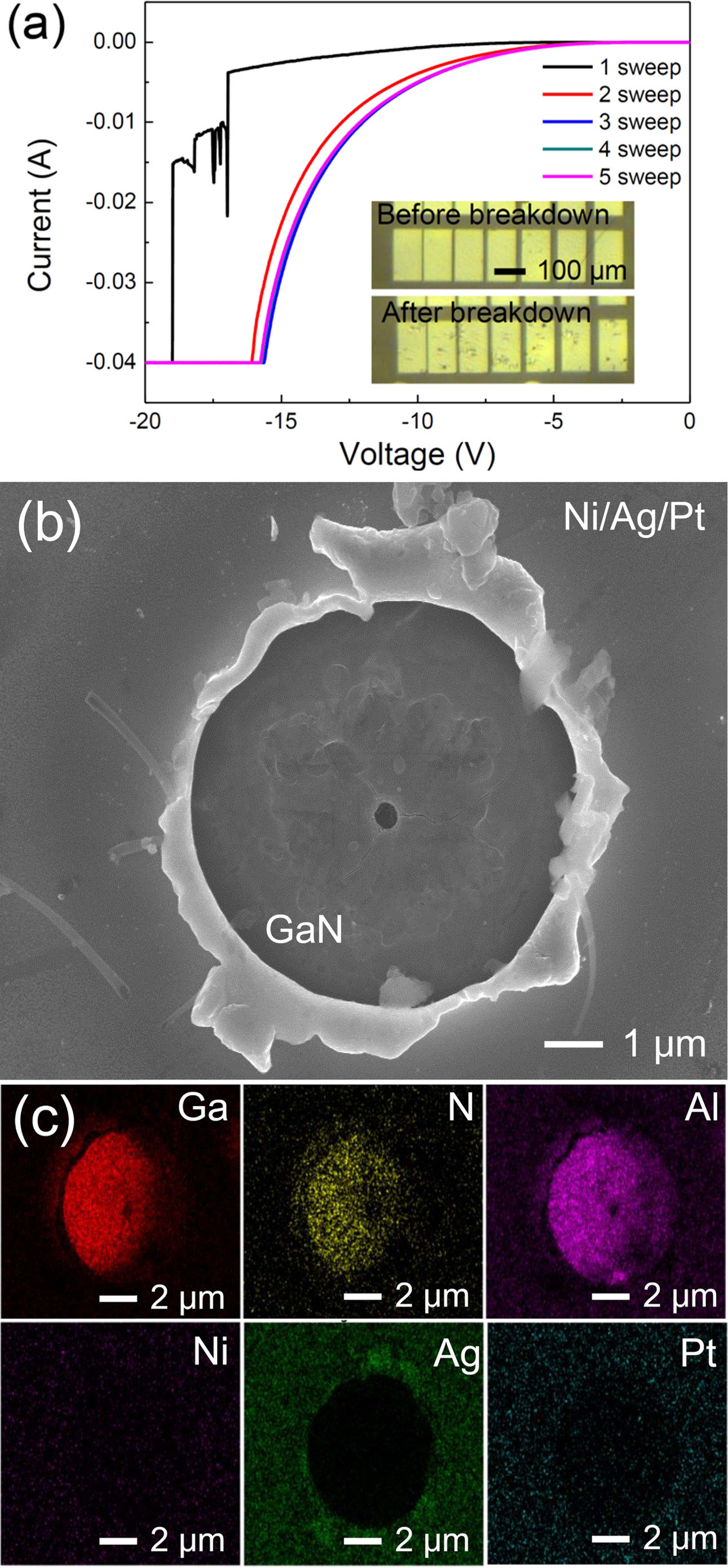
Fig. 2(a) shows the current-voltage (I-V) curves of
Ni/Ag/Pt contact formed on the top p-GaN layer as a function of reverse
biasing. For this study, the TLM patterns having the pattern size of
200 × 100 mm2 and a pad spacing of 5 μm was used (see the
inset of Fig. 2(a)). Note that the junction breakdown occurs at reverse
voltage lower than -15 V with the first I-V sweep.
The additional I-V sweeps produced an insignificant change of I-V
curve, i.e., the generation of BICCs originating from the junction breakdown through the
V-defects were nearly saturated [15, 18, 19]. As shown in the inset of Fig.
2(a), a number of black spots were observed after electrical reverse biasing.
The measurements of SEM and EDX mapping on this black spot showed
that, first, the metal electrode is exploded and, second, the BICCs were formed
through the epitaxial V-defects [15] (Fig. 2(b)). The explosion and hence the peeling-off phenomenon of metal
electrode seems to be due to the
extremely large electrical resistivity of AlGaN epitaxial films [20].
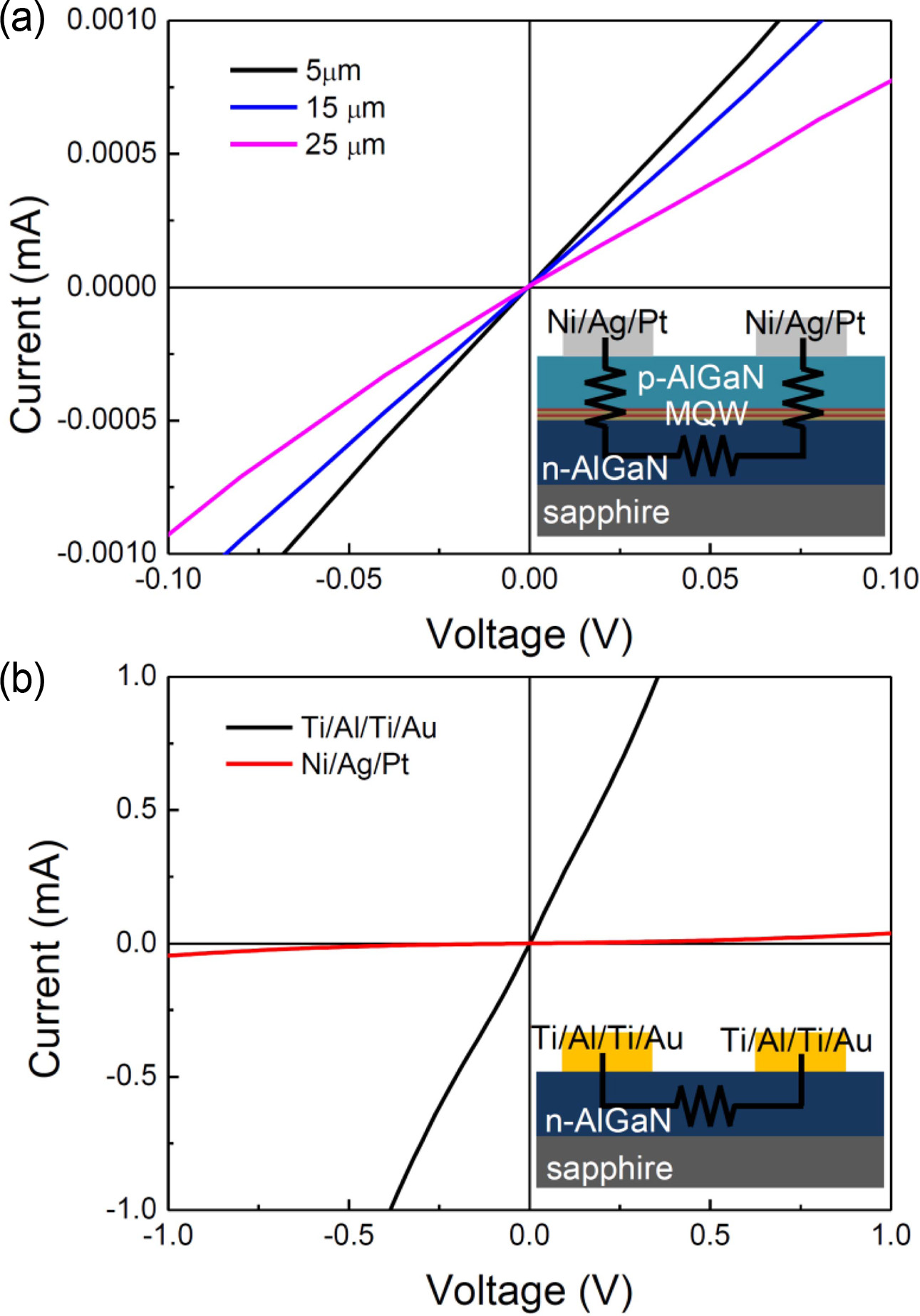
Fig. 3(a) shows I-V characteristics of the Ni/Ag/Pt
contact formed on BICCs as a function of the pad spacing. The I-V
curves showed a pad-spacing dependence, indicating that the TLM
method is valid [17]. However, the current level of contact was quite low,
resulted in the very high specific contact resistance (ρsc)
of 0.61 Ωcm2. This indicates that, although the BICCs resulted in a
current flow across junction from the top p-layer to bottom n-layer (see the
inset of Fig. 2(b)), the amount of current flow is insufficient, i.e., the
density of electrical conduction path is limited. Indeed, this is different
from our previous findings that the generation of BICCs led to a significant
current flow across the junction in the InGaN/GaN-based blue LEDs [15]. As
shown in Fig. 2(b), this is presumably due to the peeling-off of metal
electrode after BICCs formation, i.e., the although the BICCs is
generated, the conduction through BICCs would be very limited due
to the absence of metal contacts.
Fig. 3(b) shows the I-V curves of Ni/Ag/Pt formed
on BICCs and the conventional Ti/Al/Ti/Au formed on n-AlGaN layer (mesa etched
surface), where the pad spacing was 5 mm. The current flow of conventional
Ti/Al/Ti/Au contact is schematically drawn as shown in the inset of Fig. 3(b).
It is clear that the Ti/Al/Ti/Au formed on n-AlGaN layer has much steeper I-V
curve than the Ni/Ag/Pt formed on BICCs. Accordingly, the specific contact
resistance of Ti/Al/Ti/Au on n-AlGaN was measured to be
8.48 × 10⁻³ Ωcm2.
This result indicates that the contact properties of
Ni/Ag/Pt on BICCs still need to be further improved by optimizing the density
of BICCs.
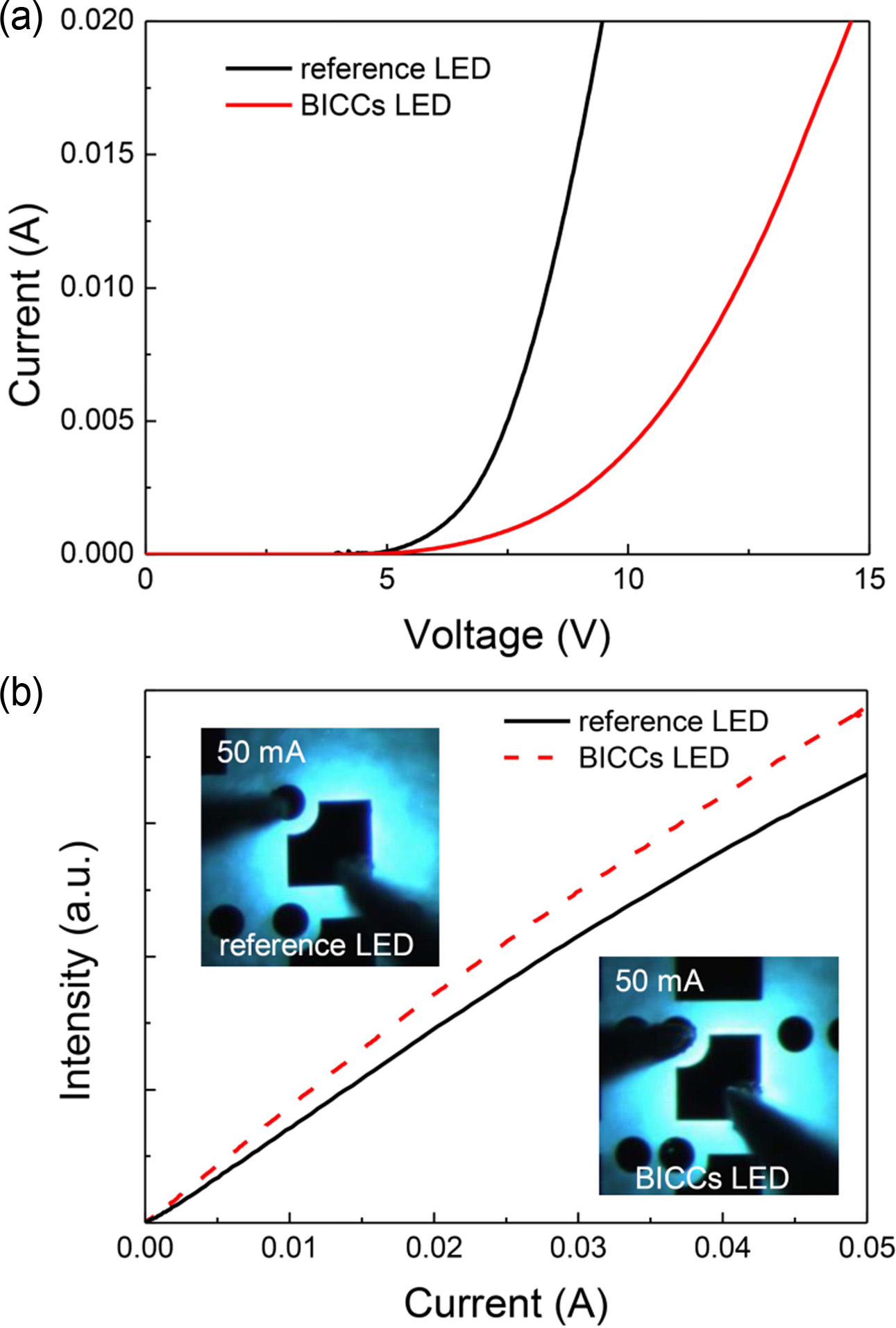
Fig. 4(a) shows the I-V curves of the reference
LEDs and the BICCs-LEDs. Consistently, the reference LEDs showed superior I-V
curves against the BICCs-LEDs. For example, the forward voltages
measured at injection current of 20 mA were 9.4 V and 14.6
V for the reference LEDs and BICCs-LEDs, respectively. This is essentially due
to the worse contact properties of Ni/Ag/Pt on BICCs over the Ti/Al/Ti/Au on
n-AlGaN.
Nevertheless, the optical output properties of the
BICCs-LEDs were significantly improved as compared to the reference LED (Fig.
4(b)). For example, the optical output power of BICCs-LEDs was about 15% higher
than that of the reference LEDs when measured at injection current 50 mA. Here,
the optical output power was measured using the photodiodes, which were placed
bottom side of LED wafers. A noticeable output enhancement is attributed to the
higher optical reflectivity of thermally annealed Ni/Ag/Pt contact than that of
annealed Ti/Al/Ti/Au.
Indeed, it is generally known that the optical
reflectivity of Ag is highest among metals in the
visible wavelength range (> 400 nm) [21].
However, the optical reflectivity of Ag drops significantly at the
wavelength below 400 nm. On the one hand, the Al metal is known to show the
highest optical reflectivity at the deep UV wavelength range
(< 300 nm), while the Ti has poor reflectivity. However, it should be
noted that the metal electrodes are thermally annealed for the formation of
Ohmic contact. During the annealing process, each metal can interdiffuse
depending on their thermodynamic tendency. In
other words, this indicates that the optical reflectivity of
electrodes should be compared after thermal annealing. Fig.
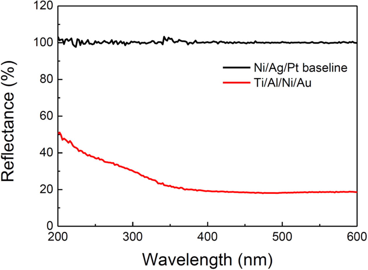
5 shows the relative optical reflectance spectra of thermally annealed Ni/Ag/Pt
and Ti/Al/Ti/Au prepared on both-side polished sapphire
substrates. For this measurements, the optical reflectance spectra of annealed
Ni/Ag/Pt were set as the base line of 100%. Note that, at the wavelength of 273
nm, the optical reflectance of annealed Ni/Ag/Pt was ~65% higher
than that of annealed Ti/Al/Ti/Au. Therefore, the enhanced
optical output power of BICCs-LEDs is explained.
|
Fig. 2 (a) I-V curves of Ni/Ag/Pt contact formed on the top p-GaN layer as a function of reverse biasing. The inset shows the optical microscopic image of the TLM patterns before and after breakdown. (b) SEM image and (c) EDX mapping images of TLM patterns after breakdown by reverse biasing. |
|
Fig. 3 (a) I-V characteristics of the Ni/Ag/Pt contact formed on BICCs-generated conduction layer as a function of the pad spacing. The inset shows the schematic cross-sectional diagram of current flow across BICCs. (b) I-V curves of Ni/Ag/Pt formed on BICCs and the conventional Ti/Al/Ti/Au formed on n-AlGaN layer. The inset shows the schematic current flow of conventional n-contact. |
|
Fig. 4 (a) Typical I-V curves of reference LEDs and BICCs-LEDs. (b) The optical output power verse current curve of reference LEDs and BICCs-LEDs. The inset show the EL image of both LEDs taken at injection current of 50 mA. |
|
Fig. 5 The relative optical reflectance spectra of thermally annealed Ni/Ag/Pt and Ti/Al/Ti/Au electrodes. |
In summary, the optical output power of AlGaN/GaN deep UV
LEDs could be improved by using reflective Ni/Ag/Pt contact and BICCs. By using
BICCs, the Ni/Ag/Pt contacts could be used as the p- and n-type electrodes
simultaneously. Besides the simpler and cost-comparative
process step, the Ni/Ag/Pt contact showed much higher optical reflectivity than
the reference Ti/Al/Ti/Au contact. Accordingly, the UV LEDs
fabricated with the Ni/Ag/Pt and BICCs produced 15% higher optical
output power than the reference LEDs. This indicates that, if the electrical
contact properties are further improved, the BICCs method combined with the use
of reflective metal contact would be promising for improving the output
efficiency of deep UV LEDs.
This work was supported by Samsung Research Funding Center
of Samsung Electronics under Project Number SRFC-IT1501-06, and by the
Technology Innovation Program (Leading design of future environment
products using advanced photocatalytic purification sterilization
technology) (Project No. 20006767) funded by the
Ministry of Trade, Industry & Energy, Republic of Korea.
- 1. M. R. Krames, O. B. Shchekin, R. Mueller-Mach, G. O.Mueller, L. Zhou, G. Harbers, and M. G. Craford, J. Disp. Technol. 3 (2007) 160-175.
-

- 2. S. Nakamura, T. Mukai, and M. Senoh, Jpn. J. Appl. Phys. 30 (1991) L1708-L1711.
-
- 3. J. J. Wierer, D. A. Steigerwald, M. R. Krames, J. J. O’Shea, M. J. Ludowise, G. Christenson, Y. C. Shen, C. Lowery, P. S. Martin, S. Subramanya, W. G. W. Götz, N. F. Gardner, R. S. Kern, and S. A. Stockman, Appl. Phys. Lett. 78[22] (2001) 3379-3381.
-
- 4. H. Kudo, M. Sawai, Y. Suzuki, X. Wang, T. Gessei, D. Takahasho, T. Arakawa, and K. Mitsubayashi, Sens. Actuator B-chem. 147 (2010) 676-680.
-
- 5. J. Close, J. Ip, K. H. Lam, Renew. Energy 31 (2006) 1657-1664.
-
- 6. J. L. Shie, C. H. Lee, C. S. Chiou, C. T. Chang, C. C. Chang, C. Y. Chang, J. Hazard. Mater. 155 (2008) 164-172.
-
- 7. M. Kneissl, T. Seong, J. Han, and H. Amano, Nat. Photonics 13 (2019) 233-244.
-
- 8. Y. Cuo, J. Yan, Y. Zhang, J. Wang, and J. Li, J. Nano- photonics 12[4] (2018) 043510.
-
- 9. H. Ryu, I. Choi, H. Choi, and J. Shim, Appl. Phys. Express 6 (2013) 062101.
-
- 10. M. Akiba, H. Hirayama, Y. Tomita, Y. Tsukada, N. Maeda, and N. Kamata, Phys. Status Solidi C. 9[3/4] (2012) 806-809.
-
- 11. P. Dong, J. Yan, Y. Zhang, J. Wang, C. Geng, H. Zheng, X. Wei, Q. Yan, and J. Opt. Express 22[S2] (2014) A320-A327.
-
- 12. S. Zhao, M. Djavid, and Z. Mi, Nano Lett. 15[10] (2015) 7006-7009.
-
- 13. N. Maeda and H. Hirayama, Phys. Status Solidi C 10[11] (2013) 1521-1524.
-
- 14. M. Shatalov, W. Sun, A. Lunev, X. Hu, A. Dobrinsky, Y. Bilenko, J. Yang, M. Shur, R. Gaska, and C. Moe, Appl. Phys. Express 5[8] (2012) 082101.
-
- 15. S. Han, S. Baek, H. Lee, H. Kim, and S. Lee, Sci. Rep. 8 (2018) 16547.
-
- 16. S. Baek, H. Lee, and S. Lee, Sci. Rep. 9 (2019) 13654.
-
- 17. G. K. Reeves and H. B. Harrison, IEEE Electron. Device Lett. 3(1982) 111-113.
-
- 18. X. H. Wu, C. R. Elsass, A. Abare, M. Mack, S. Keller, P. M. Petroff, S. P. DenBaars, and J. S. Speck, Appl. Phys. Lett. 72 (1998) 692-694.
-
- 19. H. K. Cho and J. Y. Lee, Appl. Phys. Lett. 79 (2001) 215-217.
-
- 20. S. Jeong, M. S. Kim, S. Lee, and H. Kim, Mat. Sci. Semicon. Proc. 90 (2019) 72.
-
- 21. H. Kim, K. H. Baik, J. Cho, J. W. Lee, S. Yoon, H. Kim, S. Lee, C. Sone, Y. Park, and T. Seong, IEEE Photonics Technol. Lett. 19 (2007) 336-338.
-
 This Article
-
2020; 21(S1): 23-27
Published on May 31, 2020
- 10.36410/jcpr.2020.21.S1.s23
- Received on Dec 13, 2019
- Revised on Apr 24, 2020
- Accepted on May 4, 2020
Services
- Abstract
introduction
experimental
results and discussion
conclusions
- Acknowledgements
- References
- Full Text PDF
Shared
Correspondence to
- Chel-Jong Choi and Hyunsoo Kim
-
School of Semiconductor and Chemical Engineering, Semiconductor Physics Research Center, Jeonbuk National University, Jeonju 54896, Korea
Tel : +82-63-270-3974
Fax: +82-63-270-3585 - E-mail: cjchoi@jbnu.ac.kr, hskim7@jbnu.ac.kr
Clean-Energy Research Institute(CRI), Hanyang University, 222, Wangsimni-ro, Seongdong-gu, Seoul, 04763, Korea
E-mail: jcpr@hanyang.ac.kr