


- Investigation of the electrical properties of Ag/n-Si schottky diode obtained by two different methods
Vagif Nevruzoglu*, Melih Manir and Gizem Ozturk
Department of Energy Systems Engineering, Recep Tayyip Erdogan University, 53100 Rize, Turkey
In present study, Ag/n-Si Schottky
diodes were produced by vacuum evaporation method at two different substrate
temperatures (200 K and 300 K) and structural, optical, electrical properties
were investigated. X-ray diffraction studies showed that the textures of the Ag
films are cubic with a strong (111) preferred direction. Field emission
scanning electron microscopy (FESEM) images revealed that the Ag layer coated
at 200 K substrate temperature consisted of nano clusters of equal size (12-15
nm) and the Ag layer consisted of islets of different sizes (80-100 nm) at 300
K substrate temperature. The ideal factor (n), barrier height (φB),
saturation current (I0) and series resistance (RS) for
Schottky diodes 200 K and 300 K substrate temperature produced, obtained by
using I-V measurements respectively 1.11, 0.85 eV, 0.0014 ηA, 3.45 KΩ and 3.68,
0.78 eV, 0.05 ηA, 5.51 KΩ. Donor density (ND) and flat band
potential (EFB) for Schottky diodes 200 K and 300 K
substrate temperature produced, obtained by using C-V measurements respectively
1.1 × 1015 cm-3, 0.52 V and 1.4 × 10¹⁶
cm-3, 0.34 V. When the characteristic properties of Schottky diodes
are examined, it is understood that the differences depending on the method are
caused by the distribution of homogeneous and equal sized nano clusters on the
Si surface of the Ag layer produced at 200 K substrate temperature.
Keywords: Cold substrate, Thin film, Schottky diode
Metal-semiconductor contacts (Schottky diodes) are
indispensable component of the electronics industry. Compared to P-N junction,
these devices have some advantages such as low series resistance, high power capacity
and high switching speed at low voltage values [1, 2].
The electrical parameters of an ideal Schottky diode are determined by the
properties of the metal-semiconductor interface region [3, 4]. In this
direction, metal layers are formed by different methods and an intermediate
layer is placed in the metal-semiconductor contact area
[5, 6]. Nowadays, Schottky diodes, transistor and solar
cells are produced using different methods such as thermal evaporation, spin
coater and magnetron sputtering [7-9]. Micro and nano structured materials are
becoming increasingly important in technology [10].
Ag / SiO2 / n-Si Schottky diode was produced
and examined by with vacuum evaporation technique. The electrical
characteristics of the metal-insulator-semiconductor diode and
the interface state density were evaluated by I-V and impedance spectroscopy.
They calculated the barrier height as 0.62 eV, the ideality factor as 1.91 and
the average series resistance as 975.8 Ω [11].
Bates et al. (2007) showed that Ag atoms have deposited on
the surface of n-Si at 400 and 550 oC by using magnetron sputtering
technique. They found that Ag grain size at 400 oC from TEM
images was 5 nm and 10 nm at 550 oC. In Schottky diode produced
at 400 oC, carrier density is smaller than
550 oC. However, resistance and mobility values of
Ag layer produced at 400 oC were higher than 550 oC
[12]. Mahmood et al. (2018) examined Ag / n-Si diodes by creating some of the
characteristics of these diodes with the organic interface layer and
non-interface layer. The ideality factor of the structures with non-interface
layer and the organic interface layer was 1.42 and 1.83 respectively. The size
of the barrier height was 0.65 eV for the Ag / n-Si structure and 0.66 eV for
the hybrid structure. The series resistance values of the structures with and
without organic interface layer were 7,839 Ω and 135 respectively. Donor
density was 2.07 × 1014 cm-3 in the Ag / n-Si
structure and 24.8 × 1014 cm-3 in the hybrid
structure [13]. Korosak and Cvikl (1998) used Ionized Cluster Ray (ICB) method
and obtained the Ag / n-Si Schottky structures current voltage
characteristics measured at different temperature ranges (300 K-150
K). In the examples, different current conduction mechanisms
were determined [14].
Clayton et al. (2013) revealed that Ag / n-Si composite
films produced by magnetron sputtering technique at 550 oC on
n-Si (111) substrates were characterized. Films were prepared with a
concentration of 13, 16 and 22% Ag and measured in the 77-500 K temperature
range. A decrease in resistance values was observed between the Ag
nanoparticles formed with increasing Ag concentration due to less grain
boundary. It was found that as Ag concentration increased, grain boundaries
converged and became ineffective. The barrier heights were found to be 0.360
eV, 0.390 eV and 0.470 eV for the films with Ag concentrations of 13%, 16% and
22%, respectively. As can be seen from the studies mentioned above, the
characteristics of Schottky diodes change depending on the production method
[15].
In the study conducted by Yüzüak et al. (2019), Ag layers
were grown by soliton growth mechanism on n-Si (100) substrates by using cold
substrate method [16]. Some characteristics of the diode obtained at 200 K
substrate temperature were compared with those of the diode produced at 300 K
substrate temperature.
As mentioned above, in
literature studies, the studies using cold substrate method exist. However,
based on our best knowledge, there is no a study examining the effect of this
technique on the characteristics of Ag / n-Si Schottky structures which forms
the basis of the study. Present study was realized by making use of this gap.
Recent studies have focused on the surface plasmon resonance (SPR) diffusion
model that occurs in nano size metallic particle systems [14]. This model shows
more effective diffusion of nano sized metallic particles. The advantages and
disadvantages of this model will be revealed in this dual structure we have
discussed.
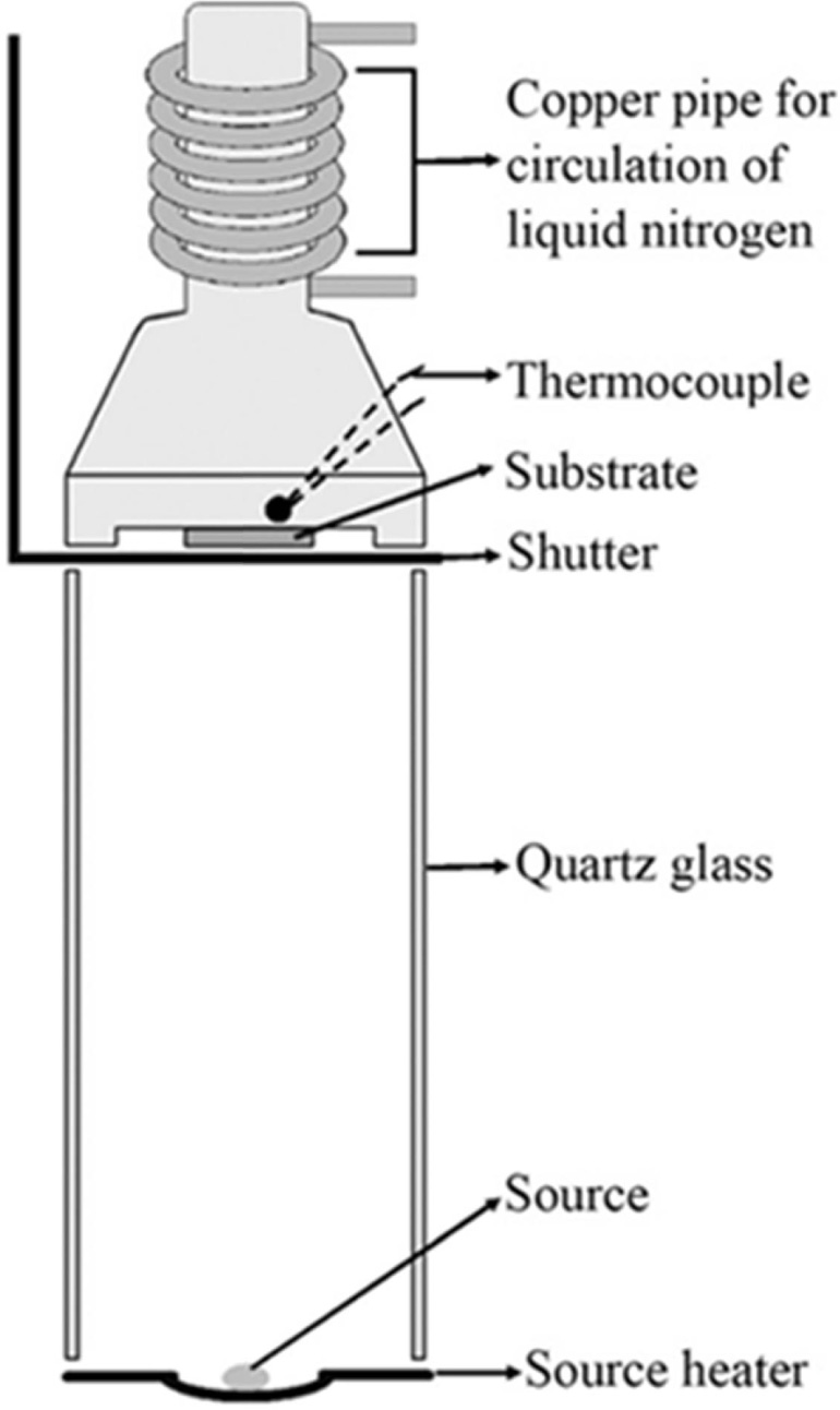
In the experiments, n-Si substrates (100) with resistivity
value of ρ = 1-10 Ω·cm and thickness of d = 375 µm were used. InGa material was
used for ohmic contact on n-Si. Ag/Si binary structures were annealed at room
conditions for 30 min at 300 °C due to the formation of diode
structure. The cold substrate method view of the evaporation apparatus is given
in Fig. 1. Substrate temperature was monitored and controlled using thermocouple. When the pressure reached
1.1 × 10⁻⁵
Torr, the substrate was cooled using liquid nitrogen. The Ag thin
films were grown at substrate temperatures of 300 K and
200 K. The shutter is continuously kept open during
deposition. The Ag thin films were deposited by vacuum
evaporation in a quasi-closed volume on n-Si substrates using high purity Ag
wire (99.99%) as the source material [16].
The crystal structure of Ag thin films was studied by X-ray
diffraction (XRD) using Rigaku SmartLab diffractometer with CuKα radiation (λ = 1,5408
Å) over the range 20o ≤2θ ≤ 80o at room temperature.
Electrical measurements of n-Si / Ag Schottky diodes were performed at room
temperature (300K) using the Ivium CompactStat.h10800 electrochemical measuring
device. Zeiss Sigma 300 was used for Field Emission Scanning Electron
Microscopy (FESEM) analysis. Changes in the Photocurrent values versus
wavelength were studied at room temperature in the range of 350-750 nm by
Monora 200 monochramator for Ag layers produced at 200 K and 300 K substrate
temperatures.
|
Fig. 1 A cross-sectional view of the thermal evaporation apparatus. |
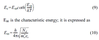
The XRD results of the Ag films on n-Si substrates at
temperatures of 300 K and 200 K are shown in Fig. 2. X-ray was sent to the
substrate surface at angle of 1o and reflected from the Ag thin
film. It was found from the XRD patterns that the reflection intensity of the
substrate evaporated in Ag layer at 200 K temperature was higher than substrate
evaporated at 300 K. This phenomenon is due to forming a tight package on the
n-Si surface for the Ag coated substrate at temperature of 200 K. The peaks of
Ag layers at angles 2θ = 38.2o, 44.3o, 64.5o and
77.6o belonged to (111), (200), (220) and (311) planes respectively.
In addition, it was seen that the Ag thin film was in line with the preferred
growth orientation (111) and had a cubic structure [17]. The peaks seen in the
XRD pattern were compared with the PDF Card No: 1100136 data card. However, in
the spectrum 2θ= 55o, Si (100) plane reflection was detected.
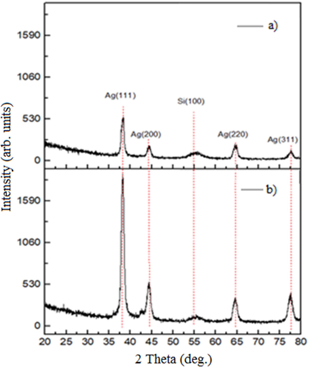
Fig. 3 shows the FESEM image of Ag thin films produced on
a glass surface for substrate temperature at 200 K and 300 K. In Fig. 3(a), at
300 K production temperature, Ag layer is
composed of islets of different sizes and in Fig. 3(b), at 200 K production
temperature, Ag layer is composed of equal sized clusters [18]. This result
shows that the Ag layer at substrate temperature of 200 K is caused by soliton
growth mechanism.
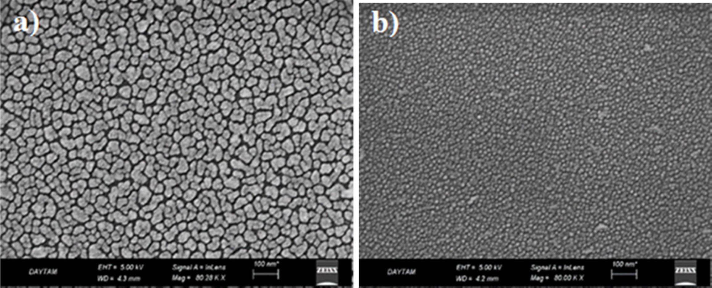
As it is known, superficial plasmon resonance (SPR) event
occurs in nano-sized Ag layers at a certain frequency [19]. In order to
determine this, the changes in the photocurrent values according to the
wavelength of Ag layers formed on the insulating glass surface at 300 K and 200 K
substrate temperatures were examined. Fig. 4
shows the photocurrent value of the Ag film produced at a substrate temperature
of 200 K at a wavelength of 470 nm [19]. The wavelength at which the SPR event
occurs corresponds to 638 THz. It is known from the literature that the SPR
event in the Ag structure has a frequency of 638 THz [14]. At 300 K substrate temperature, there is no interesting
situation in the photocurrent values
with varying wavelengths.
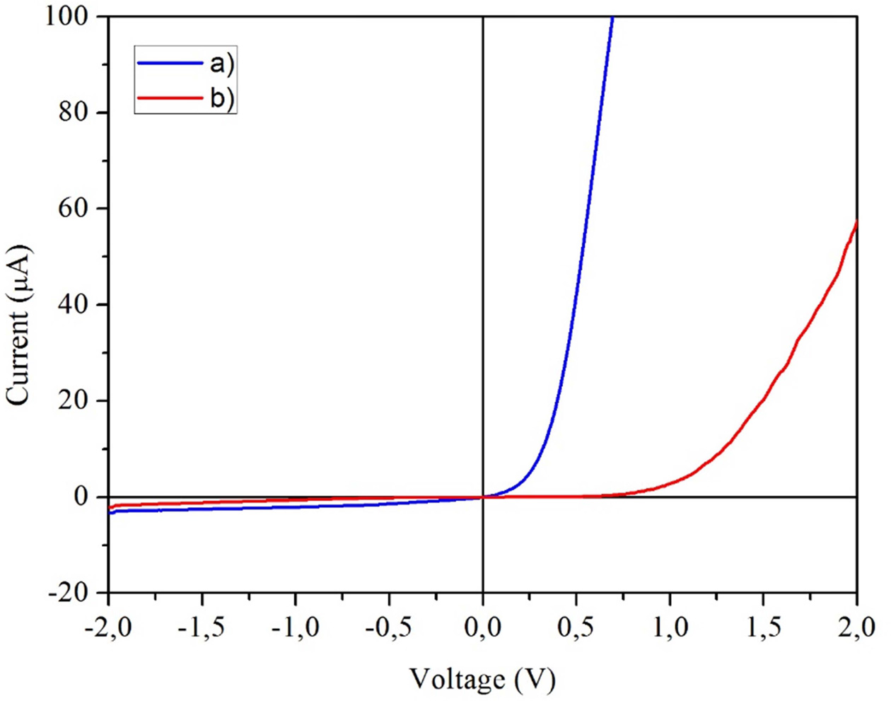
Fig. 5 shows the I - V measurement results of n-Si / Ag
Schottky diodes produced at substrate temperature of 200 K and 300 K. As can be
seen, both examples show rectifier characteristics. The n-Si / Ag Schottky diode
produced at a substrate temperature of 200 K showed sharper rectifier
properties. This was due to reduction in surface state density in the metal-semiconductor
contact region of the diode produced at a substrate temperature of 200 K.
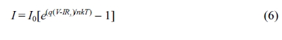
The thermionic emission current-voltage relation of a
Schottky diode is given by [20]
where I0 is the
saturation current, q is the electronic charge, V is the applied
voltage, n is the ideality factor, k is Boltzmann’s constant and T
is the temperature in K. The saturation current I0 is
defined by
where A* is the
theoretical Richardson constant (A* = 112 A/cm2K2 for
n-Si), A is the diode area and fb
is the zero bias barrier height. For V values greater than 3 kT/q, the ideality
factor n can be calculated from the slope of the rectification line region of
the forward bias ln(I)-V plot for each temperature and can be written as

I0 can be
determined by an extrapolation of the forward bias ln(I)-V
curve to V = 0 for each temperature. The zero bias
barrier height (fb)
is calculated by the following formula:
The expression for the interface state density as deduced
by Card and Rhoderick [21] is reduced to
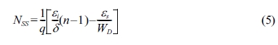
where d is the thickness of
interfacial insulator layer, WD is the width of the space
charge region, εi and εs are the
permittivity of the interfacial insulator layer and the semiconductor,
respectively.
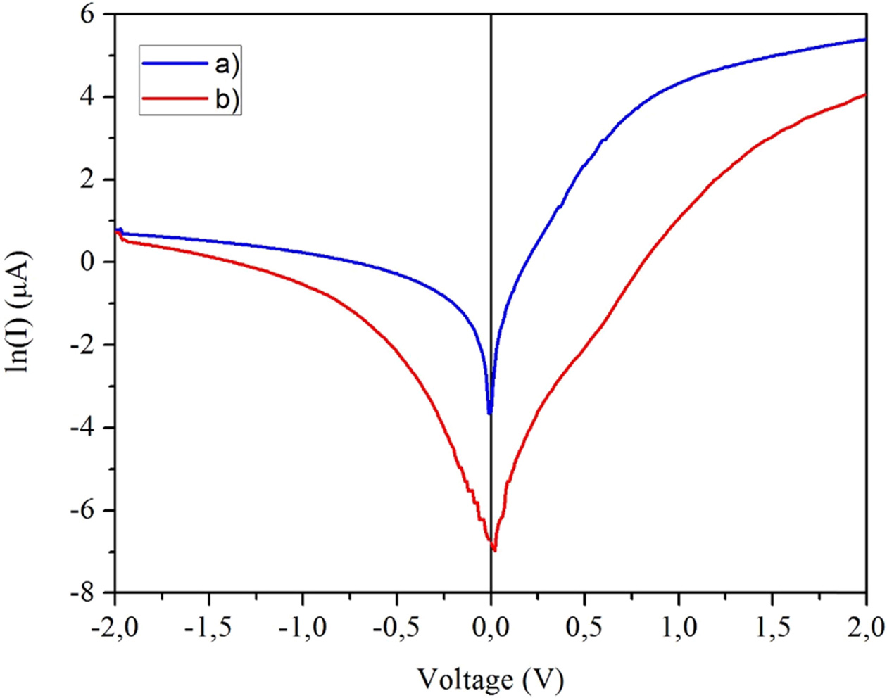
In Fig. 6, the semi-logarithmic I-V graph of n-Si /Ag
Schottky diodes was produced at 200 K and 300 K substrate temperatures. The ln
(I) -V curve of the n-Si / Ag Schottky diode produced at substrate temperature
of 300 K shows a linear behavior between bias voltages of 0.2-1.5 V, while the
diode produced at substrate temperature of 200 K shows a linear variation in
the range of bias voltages of 0-0.7 V [18].
In Table 1, ideality factor (n) and saturation current (I0)
values of n-Si / Ag Schottky diodes produced at 200 K and 300 K substrate
temperatures were calculated from ln (I)-V graph. As can be seen from the Table
1, Schottky diode at 300 K substrate temperature has higher n and I0
values than 200 K substrate temperature production. However, the barrier height
(φB) of the diode at a substrate temperature of 300 K is lower than
that produced at 200 K. As is known, at a substrate temperature of 300 K, the
Si surface Ag layer is coated with islets of different sizes. Thus,
non-homogeneous regions were formed at the interface of the Si / Ag Schottky
barrier [22-25]. This leads to a reduction in the barrier
potential at the metal-semiconductor interface [26, 27].
The ideality factors of the samples are greater than 1,
indicating that there are different current conduction mechanisms in the
diodes.
The thermionic emission current-voltage relation of a
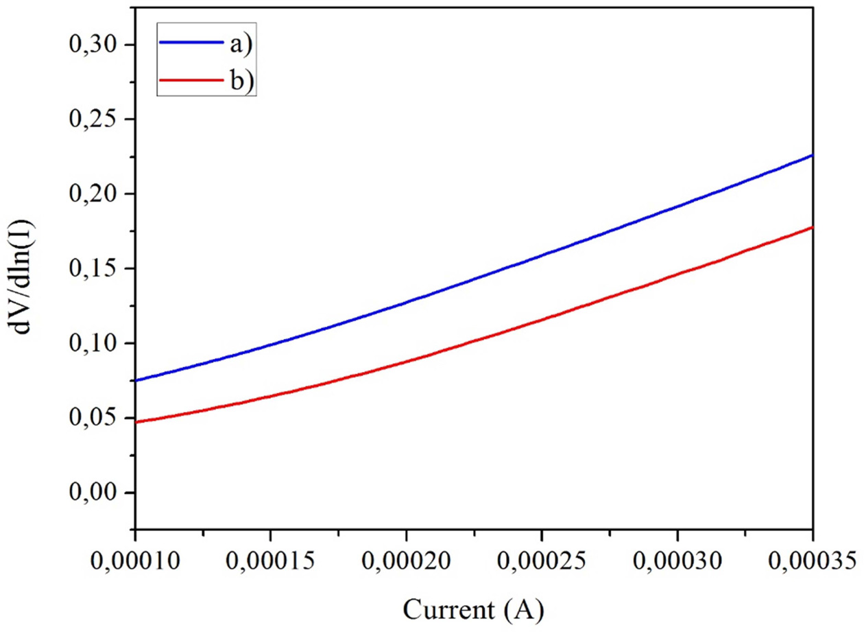
Schottky diode with series resistance is given by [20]
where Rs is serial
resistance. Eq. (6) can be differentiated as follows:
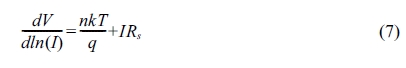
The series resistances are evaluated by using the slopes
of dV/dln(I) versus I curves. Fig. 7 shows dV/dln(I) versus I plots for the
n-Si/Ag (at 200 K and 300 K) Schottky diode.
From the experimental results, series resistance values
of diodes were found. In Table 1, series resistance values are calculated from
dV/dln (I) graph and are given. It is seen in the Table 1 that the diode
prepared at 300 K substrate temperature has higher series resistance values
than the diode prepared at 200 K substrate temperature. Increases in series
resistance values are due to increases in surface state density in the
metal-semiconductor interface area [28, 29].
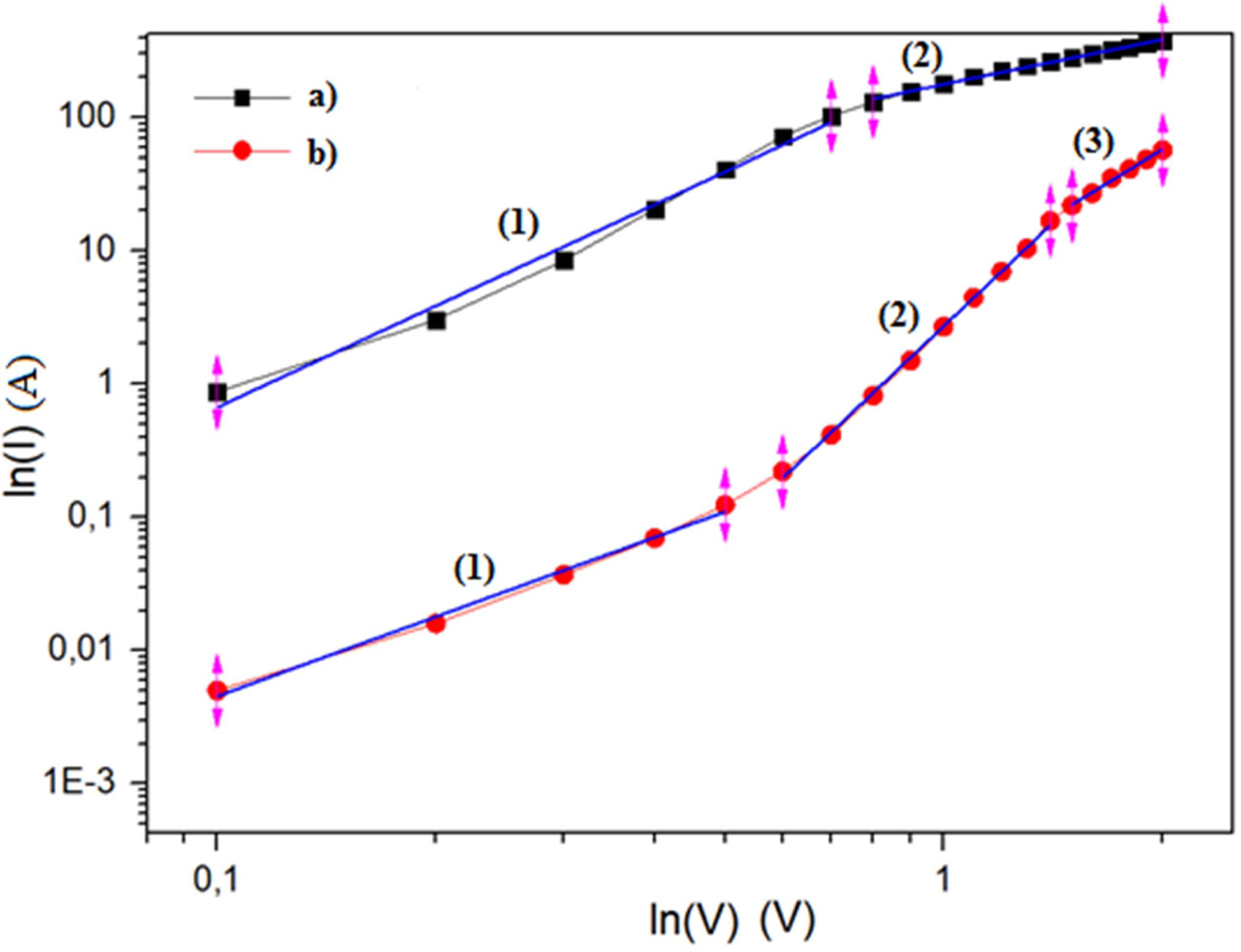
Double Logarithmic I-V graph (Fig. 8) was used to
determine the conduction mechanisms of the produced Si / Ag
Schottky diodes. In Fig 8, Schottky diode produced at
300 K substrate temperature, 3 separate linear regions, two
separate linear regions produced at 200 K substrate temperature were seen.
Since the first region slope (m) of both diodes is greater than 2, the space
charge limited current mechanism (SCLC) is effective in this region. In the
second region, m <2 and omics behavior is exhibited. This shows that the
tunneling current mechanism is dominant in the second region. In the third
region of the Schottky diode produced at a substrate temperature
of 300 K, m > 2, the Space Charge Limited Current
mechanism (SCLC) is effective in this region.
In practice, tunneling mechanism is very significant for
semiconductors that have E00 =10 value or a doping level
higher than ~1 × 1017 cm-3
[10]. The carrier density of Schottky diode at substrate
temperature of 300 K was found to be 1.1 × 10¹⁷
cm-3.
Therefore, the tunneling mechanism was investigated for
n-Si/Ag structure. Tunneling mechanism can occur as two mechanisms: (1)
field emission (FE) and (2) thermionic field emission (TFE). TFE
theory is the dominant mechanism in the intermediate temperature and doping
concentration, but FE theory is dominant only at quite low temperatures for the
material having high doping concentrations [23]. Current-voltage relation for
tunneling mechanism is given by [30,31]
Where
According to the theory, if E00 >> kT
is FE dominant, E00 ~ KT is TFE dominant, and E00 << kT
is thermionic emission diffusion mechanism is dominant. In the Si / Ag
Schottky diode produced at 200 K substrate temperature according to E00
values given in Table 1, it is found that the field thermionic emission
diffusion mechanism is dominant. The field emission mechanism is dominant in
the Si-Ag Schottky diode produced at a substrate temperature of 300 K.
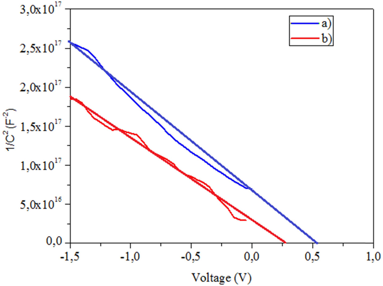
Fig. 9 shows the Mott-Schottky graph measured at 1000 Hz
frequency for Schottky diodes produced at 200 K and 300
K substrate temperatures. Typical results of C/V
measurements for both types of diodes are displayed in Fig. 9. The constant
slopes of the 1/C2 versus V curves indicate uniform doping profiles of the substrates and abrupt interfaces. Ideally, the capacitance (C) of a Schottky barrier is expressed from Eq.
(11) [32, 33].

Where V is the applied potential, S is the active device
area, Nd is the donor concentration, Vd is the diffusion
potential, ε0 is the vacuum dielectric constant and the relative
dielectric constant εs. Where the curve in the graph is 1 / C2 = 0
gives us the flat band potential (VFB). Table 1 shows the VFB
values of Schottky diodes produced at 200 K and 300 K substrate temperatures. Donor
densities in Si/Ag Schottky diodes were determined from linear
regions of Mott Schottky curves.
Table 1 shows ND, VFB and NSS
values calculated from C-V measurements. The donor density was found to be
lower at the 200 K substrate temperature than the 300 K substrate temperature.
The surface state density (NSS) at the
metal-semiconductor interface was calculated to be lower
in the Schottky diode produced at a substrate temperature of 200 K compared to
a substrate temperature of 300 K.
|
Fig. 2 XRD patterns of n-Si/Ag prepared binary structure at (a) 300 K and (b) 200 K. |
|
Fig. 3 FESEM image of glass/Ag thin films (a) 300 K and (b) 200 K. |
|
Fig. 4 Wavelength-current graph at (a) 300 K and (b) 200 K. |
|
Fig. 5 I-V graph of n-Si/Ag Schottky barriers at (a) 200 K and (b) 300 K. |
|
Fig. 6 Semi-logarithmic I-V graph of n-Si/Ag Schottky diode at (a) 200 K and (b) at 300 K. |
|
Fig. 7 Experimental dV/dln(I) versus I plots for the n-Si/Ag Schottky diode at (a) 200 K and (b) 300 K. |
|
Fig. 8 Double logarithmic forward bias I-V plots of a n-Si/Ag Schottky diode at (a) 200 K and (b) 300 K. |
|
Fig. 9 Mott-Schottky graph of Si/Ag Schottky diodes (a) 200 K and (b) 300 K. |

In this study, Schottky diodes were produced by
evaporating Ag onto n-Si using vacuum evaporation technique at 200 K (cold
substrate) and 300 K substrate temperature. It was seen from the FESEM images
that the Ag layer was composed of equal sized nano clusters at 200 K substrate
temperature and that the Ag layer was composed of islets of different size at
300 K substrate temperature. When the photocurrent values were examined
according to wavelength, SPR effect was observed in Ag thin film produced at
200K substrate
temperature at 470 nm wavelength (638 THz).
Si/Ag Schottky diode produced at 200 K substrate temperature from I-V measurements had better rectification properties. In the experiments, n, I0
and Rs values of Schottky diode produced at 300K substrate temperature were
higher than those produced at 200 K substrate temperature. It was understood
from the obtained results that transmission at 200 K and 300 K substrate
temperatures can be controlled by tunneling at low bias voltages and SCLC at
high bias voltages.
- 1. S.M. Sze, in “Semiconductor Devices: Physics and Technology”, (John Wiley & Sons, 2008) p. 84.
- 2. B. Sahin, H. Cetin, and H. Ayyildiz, Solid State Commun. 135 (2005) 490-495.
-

- 3. S. Karatas, Microelectron. Eng. 87 (2010) 1935-1940.
-
- 4. M.E. Aydin, K. Akkilic, and T. Kilicoglu, Physica B. 352 (2004) 312-317.
-
- 5. Z. Ahmad and M.H. Sayyad, Physica E. 41 (2009) 631-634.
-
- 6. S. Guduru, V.P. Singh, S. Rajaputra, S. Mishra, R. Mangu, and St. Omer, Thin Solid Films 518 (2010) 1809-1814.
-
- 7. V. Nevruzoglu, M. Tomakin, E.F. Keskenler, and G. Ozturk, J. Ceram. Process. Res.18 (2017) 494-500.
- 8. F.K. Konana, A. Betiéd, H.J.T. Nkuissib, K. Dakshib, B. Akaa, and B. Hartitib, J. Ceram. Process. Res. 18 (2017) 882-886.
- 9. M. Amuthasurabi, J. Chandradass, V.R. Babu, P.B. Sethupathi, and M.L.J. Martin, J. Ceram. Process. Res. 18 (2017) 815-818.
- 10. E. Bingöl, F. Bozali, E.F. Keskenler, V. Nevruzoğlu, and M. Tomakin, Turk. J. Mater 1 (2016) 19-24.
- 11. M. Okutan and F. Yakuphanoğlu, Microelectron. Eng. 85 (2008) 646-653.
-
- 12. C.W. Bates, J.C. White, and C. Ekeocha, 143 (2007) 38-41.
-
- 13. O.H. Mahmood, A.G. İmer, and A. Korkut, ICSMD-2018, 1 (2019) 47-51.
- 14. D. Korosak and B. Cvikl, ASDAM '98, 1 (1998) 137-140.
-
- 15. W. Clayton, J. Bates, and C. Zhang, Aip Advances 3 (2013) 1-15.
-
- 16. G.D. Yüzüak, E. Yüzüak, V. Nevruzoğlu, and İ. Dinçer, Applied Physics A. 125 (2019) 794-803.
-
- 17. F. Heıdarpour, W.A. Wan, AB Karım Ghanı, F.R. Bın Ahmadun, S. Sobrı, M. Zargar, and M.R. Mozafarıa, Dig. J. Nanomater. Bios. 5 (2010) 787-796.
- 18. M. Tomakin, M. Altunbaş and E. Bacaksız, Physica B. 406 (2011) 4355-4360.
-
- 19. K.C. Lee, S.J. Lin, C.H. Lin, C.S. Tsai, and Y.J. Lu, Surf. Coat. Technol. 202 (2008) 5339-5342.
-
- 20. D.K. Schroder, in “Semiconductor Materials and Device Characterization”, (Wiley, New York, 1990) p. 190.
- 21. H.C. Card and E.H. Rhoderick, J. Phys. D: Appl. Phys. 4 (1971) 1589-1601.
- 22. R.T. Tung, Mater. Sci. Eng. R: Rep. 35 (2001) 1-138.
-
- 23. S. Oktik, G.J. Russell, and J. Woods, Semicond. Sci. Technol. 2l (1987) 661-665.
-
- 24. K. Patel, K.K. Nanda, and S.N. Sahu, J. Appl. Phys. 85 (1999) 3666-3670.
-
- 25. V.V. Kislyuk, M.I. Fedorchenko, P.S. Smertenko, O.P. Dimitriev, and A.A. Pud, J. Phys. D: Appl. Phys. 43 (2010) 185301-185311.
-
- 26. R.T. Tung, Phys. Rev. B 45 (1992) 13509-13523.
-
- 27. J.H. Werner and H.H. Guttler, J. Appl. Phys. 69 (1991) 1522-1533.
-
- 28. A. Keffous, M. Siad, S. Mamma, Y. Belkacem, C.L. Chaouch, H. Menari, A. Dahmani, and W. Chergui, Appl. Surf. Sci. 218 (2003) 336-342.
-
- 29. J.H. Lee, J.S. Yi, K.J. Yang, J.H. Park, and R.D. Oh, Thin Solid Films 431 (2003) 344-348.
-
- 30. F.A. Padovani and R. Stratton, Solid-State Electron 9 (1966) 695-707.
-
- 31. C.R. Crowell and V. L. Rideout, Solid-State Electron 12 (1969) 89-105.
-
- 32. S.M. Sze, in “Physics of Semiconductor Devices” (Wiley Eastern Limited, 3rd edition, 1985) p. 170.
- 33. E.H. Rhoderic and R.H. Williams, in “Metals Semiconductor Contacts” (Oxford University Press, 1988) p. 48.
 This Article
-
2020; 21(2): 256-262
Published on Apr 30, 2020
- 10.36410/jcpr.2020.21.2.256
- Received on Jan 15, 2020
- Revised on Mar 19, 2020
- Accepted on Mar 20, 2020
Services
Shared
Correspondence to
- Vagif Nevruzoglu
-
Department of Energy Systems Engineering, Recep Tayyip Erdogan University, 53100 Rize, Turkey
Tel : +90 464 2237518 Fax: +90 464 2237514 - E-mail: vagif.nevruzoglu@erdogan.edu.tr
Clean-Energy Research Institute(CRI), Hanyang University, 222, Wangsimni-ro, Seongdong-gu, Seoul, 04763, Korea
E-mail: jcpr@hanyang.ac.kr