


- Characterization of CuIn1-xGaxSe2 films prepared by spin-coating and co-reduction method
Jing Li, Kegao Liu*, Qilei Sun, Zhigang Wang and Haiyang Wu
School of Materials Science and Engineering, Co-Innovation Center for Green Building of Shandong Province, Shandong Jianzhu University, Fengming Road, Jinan 250101, China
CuIn1-xGaxSe2
film has excellent photovoltaic performance due to its large optical absorption
coefficient and direct-band gap. It was prepared by spin-coating and chemical
co-reduction method which is a simple and easy way with low cost in this work.
The surface morphology of the product film was observed using scanning electron
microscope (SEM). The absorbance curves are measured by visible
spectrophotometer. The phases of the samples were characterized by X-ray
diffraction (XRD). It was found by phase analysis that prolonging the reaction
time and increasing the reaction temperature were beneficial to the sample
crystallization. With the doping concentration increasing, the surface
morphology of CuIn1-xGaxSe2 films changed with
a tendency from spherical crystals to rods. The effect of doping concentration
on the resistivity is not particularly obvious. As the doping concentration
increases, the resistivity will increase slightly; When x=1, the resistivity
changes greatly, which may be due to the poor film continuity. Their estimated
band gaps of CuIn1-xGaxSe2 films are 1.25 eV,
1.3 eV, 1.33 eV, 1.38 eV and 1.4 eV respectively.
Keywords: CuIn1-xGaxSe2, morphology, band gap, photovoltaic, solar cell
The optimal band gap for a single junction solar cell is
about 1.4 eV. Pure CuInSe2 with a gap 1.04 eV has excellent
photoelectric performance [1,2]. Doping is an
important means to regulate the properties of materials [3-5], the
enhancement of the thermoelectric properties of the SrTiO3 by doping
with Zr were investigated [6]. To increase the width of CuInSe2
band gap, indium can be partially replaced by gallium and
then it can obtain the compound of
copper indium gallium diselenide (CIGSe). CIGSe
polycrystalline thin film is recently being developed as an
absorber material for thin-film photovoltaic solar cells, it is a
multi-crystalline semiconductor of p-type with
high-quality characteristics, such as its large optical absorption
coefficient and direct-band gap [7]. Light trapping was studied in ultrathin
CuIn1-xGaxSe2 solar cells by dielectric
nanoparticles [8]. CuInSe2 nanowire arrays with core-shell structure
were electrodeposited at various duty cycles into anodic
alumina templates [9]. The influence of process parameters
were investigated on the gallium composition of a CuIn1-xGaxSe2
solar cell [10]. It reported the effects of substrate
temperatures in the three-stage growth of CuIn1-xGaxSe2
thin films and their photovoltaic performances [11]. The structural
and optical properties of Cu-poor CuIn1-xGaxSe2
films with different gallium contents prepared by co-evaporated technique were studied
[12]. The effect of growth conditions on the
properties of sputtered precursor thin films for CuIn1-xGaxSe2
(CIGS) absorber layers was reported
[13]. Single phase polycrystalline copper indium gallium diselenide thin-films for solar photovoltaic applications were fabricated by an economical
two-stage method of pulsed current
electrodeposition [14]. Other research
works include simulations about CuIn1-xGaxSe2 alloys [15], 3-stage deposition of CuIn1-xGaxSe2
on Mo-coated glass and stainless steel
substrates [16], CuIn1-xGaxSe2 nanopowders or
nanoparticles produced by solvothermal
method [17, 18] and CuIn1-xGaxSe2 prepared by electrodeposition [19]. It has
reported our work about CuInSe2 films prepared from chlorides under
different conditions [20]. Quaternary compound CuIn1-xGaxSe2 was prepared by
spin-coating and chemical
co-reduction method in this work.
The corresponding amounts of raw materials were weighed
according to the stoichiometric ratio of CuIn1-xGaxSe2,
the precursor solution with the highest concentration
was prepared, and the mixture was shaken by the
ultrasonic cleaner to make it uniformly mixed. The CuIn1-xGaxSe2
precursor film was prepared by spin-coating with 3,000 rpm for 10 seconds, and
then the sample was placed in a reaction vessel containing hydrazine hydrate
for heat treatment at a certain temperature. Then the CuIn1-xGaxSe2
film sample was obtained after soaking in ionized water for 24 h and drying at
room temperature. The surface morphology of the product film was observed using
scanning electron microscope (SEM). The absorbance curves are measured by Model
723PC visible spectrophotometer made by Shanghai Precision Instrument Co., Ltd.
According to the light absorption characteristics of the absorbance curve in
the visible light region, the band gap widths of the CuInSe2 film samples
were estimated using extrapolation. The phases of the samples were
characterized by X-ray diffraction (XRD).
CuIn1-xGaxSe2
films were prepared by spin-coating and chemical co-reduction method
The phases of CuIn1-xGaxSe2
films prepared by different reaction time
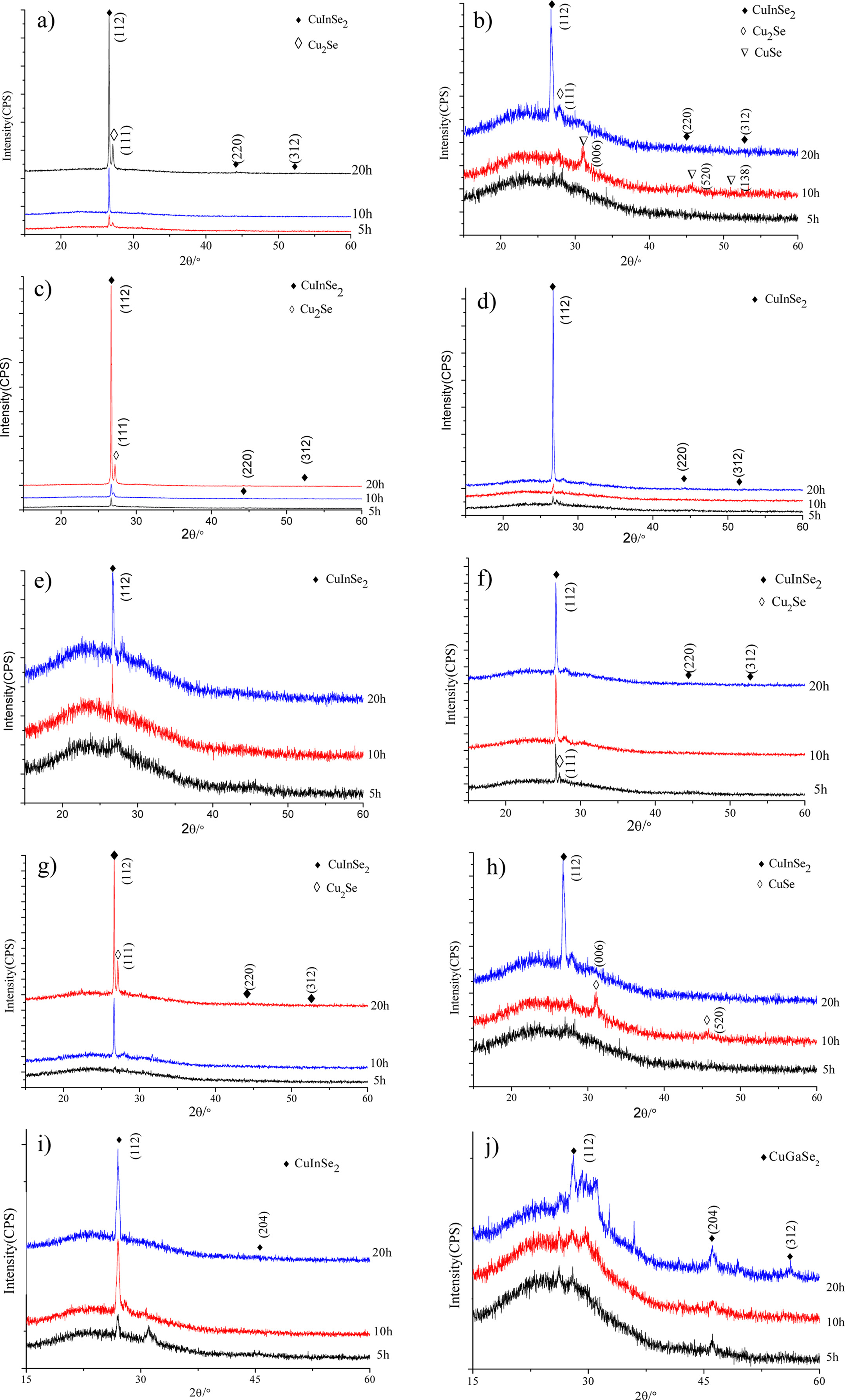
Fig. 1 shows the XRD patterns of CuIn1-xGaxSe2
obtained with different reaction time of 5 h, 10 h and 20 h at 220 °C. It
can be seen that the samples with long reaction time have higher XRD peak
intensities, and the reaction time extension is favorable for the
crystallization of the film samples. Compared with the standard PDF card with
No.89-5649, the XRD patterns of the CuIn0.9Ga0.1Se2
film samples in Fig.1a show three high peaks with 2θ angles at 26.67°, 44.32°
and 52.47° that correspond to the (112), (220) and (312) crystal planes
respectively; According to the standard PDF card with No.88-2043, the XRD peak
of impurity phase Cu2Se appears in Fig. 1(a), where the 2θ angle
27.12° corresponds to the (111) crystal plane. Fig. 1(b) indicates that the
CuIn0.8Ga0.2Se2 film samples reacted with 5 h
and 10 h have no XRD peaks corresponding to the target phase while the XRD
intensity are very low. The target XRD peaks occur in the sample with the
reaction time 20 h; Impurity CuSe appeared in the sample obtained with reaction
time 10 h. Fig. 1(c) and (d) show the XRD patterns of CuIn0.7Ga0.3Se2
and CuIn0.6Ga0.4Se2 film samples, compared
with the standard PDF card with No.89-5649,
the XRD peak positions with 2θ angles are slightly shifted to the right, while
the impurity phase Cu2Se also appeared in the sample reacted for 20
h in Fig. 1(c). It can be seen from Fig. 1(e) that the XRD intensities for the
target phase of the CuIn0.5Ga0.5Se2 sample are
lower than others and increase with the reaction time prolongation. CuIn0.4Ga0.6Se2
film samples with good crystallinity are obtained under different reaction
conditions as shown in Fig. 1(f). It can be seen from Fig. 1(g) that the CuIn0.3Ga0.7Se2
sample with reaction time 5 h has no XRD peaks. As the reaction time increases
to 10 h and 20 h, the CuIn0.3Ga0.7Se2 sample
crystallizes better and better, but impurity phase Cu2Se appeared
when 20 h. Fig. 1(h) shows that the CuIn0.2Ga0.8Se2
samples did not show the XRD peaks of the target phase with the reaction time 5
h and 10 h, and the XRD peak appeared when the reaction time extended to 20 h. Compared
with the standard PDF card No.89-5649 in Fig. 1(i), the 2θ angle positions of
XRD peaks for the CuIn0.1Ga0.9Se2 samples are
shifted to the right as a whole. The XRD peaks of the CuGaSe2 sample
correspond to the standard PDF card with
No.31-456, and the 2θ angles with
27.7°, 46.11° and 54.25° correspond
to (112), (204) and (312) crystal planes of CuGaSe2 respectively as
shown in Fig. 1(j).
Phases of CuIn1-xGaxSe2
films prepared at different reaction temperatures
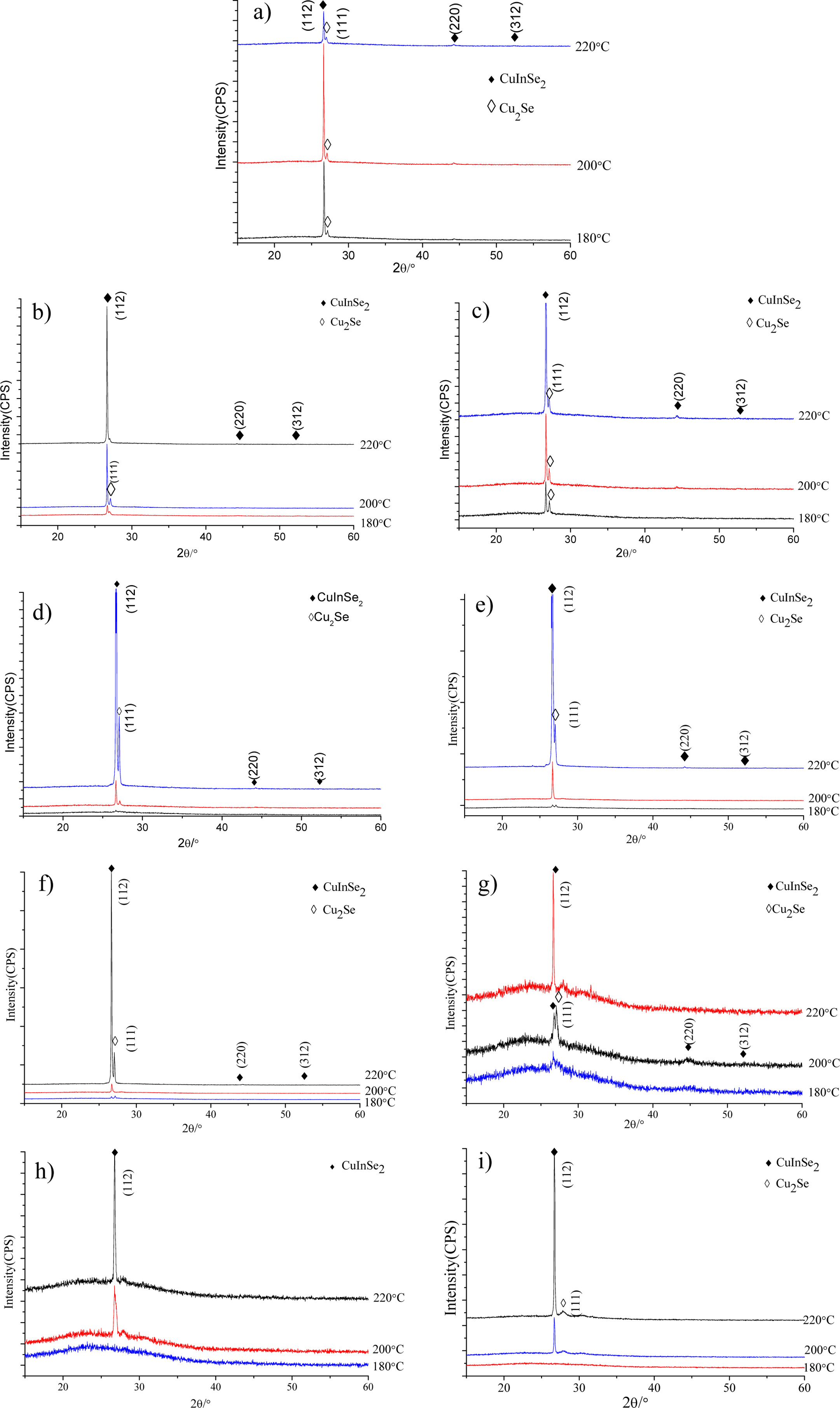
Fig. 2 shows the XRD patterns of CuIn1-xGaxSe2
samples reacted at different temperatures for 20 h, compared with
the standard PDF card with No.89-5649, the XRD peaks of 2θ
angles of 26.67°, 44.32° and 52.47° correspond to
(112), (220) and (312) crystal planes respectively. It can be seen
from Fig. 2(a) that CuIn0.9Ga0.1Se2 film samples
are all with better crystallinity obtained at three
temperatures, but impurity phase Cu2Se also appears, among
which CuIn0.9Ga0.1Se2 sample prepared at
200 °C has best crystallinity. Fig. 2(b) indicates that CuIn0.8Ga0.2Se2
film samples have impurity phase Cu2Se while the
sample with best crystallinity was obtained at 220 °C. Fig. 2(c) and Fig.
2(d) show that the XRD peak intensity and sharpness of CuIn0.7Ga0.3Se2
and CuIn0.6Ga0.4Se2 samples prepared at
220 °C are significantly higher than others, but Fig. 2(d) shows a higher
XRD peak for impurity phase Cu2Se. Fig. 2(e) and Fig. 2(f) show that
the XRD peak intensities of CuIn0.5Ga0.5Se2
and CuIn0.4Ga0.6Se2 samples prepared at
220 °C are significantly higher than those obtained at 180 °C
and 200 °C while impurity phase Cu2Se appears
at 220 °C. Fig. 2(g) shows that the XRD intensity of the CuIn0.3Ga0.7Se2
sample prepared at 180 °C is very low and become greatly high for the
sample obtained at 220 °C. Fig. 2(h) shows that there are no obvious XRD
peaks for CuIn0.2Ga0.8Se2 sample prepared at
180 °C, which indicates that no target phase appears, when the reaction
temperatures were raised to 200 °C and 220 °C
respectively, the XRD peaks for target phase appeared, the film
sample prepared at 220 °C has higher XRD peak intensity and better
crystallinity. Fig.2i shows that CuIn0.1Ga0.9Se2
film sample obtained at 220 °C has higher XRD peak intensity and better
crystallinity.
Comparison of XRD patterns of CuIn1-xGaxSe2
prepared at 220 °C for 20 h
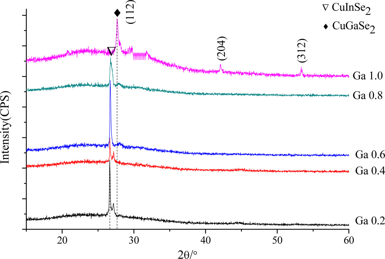
Fig. 3 shows the XRD patterns of CuIn1-xGaxSe2
with doping concentrations of 0.2, 0.4, 0.6 and 0.8 and 1.0 prepared at
220 °C for 20 h. It can be seen that, as the Ga doping concentration
increases, the characteristic XRD peaks of the samples gradually shift toward
the large diffraction angles. For example, as shown along the (112) crystal
plane, the 2θ angle of CuGaSe2 is about 0.57° larger than that of
CuIn0.8Ga0.2Se2.
Analysis of electrical properties of CuIn1-xGaxSe2
films
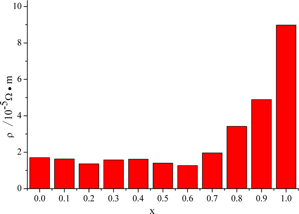
The resistivities of CuIn1-xGaxSe2
films are shown in Fig. 4, and the influence of doping concentration on the
resistivity are not obvious. As the doping concentration increases,
the resistivity will increase slightly, and when x=1, the
resistivity changes greatly, it may be due to poor continuity of the film
sample.
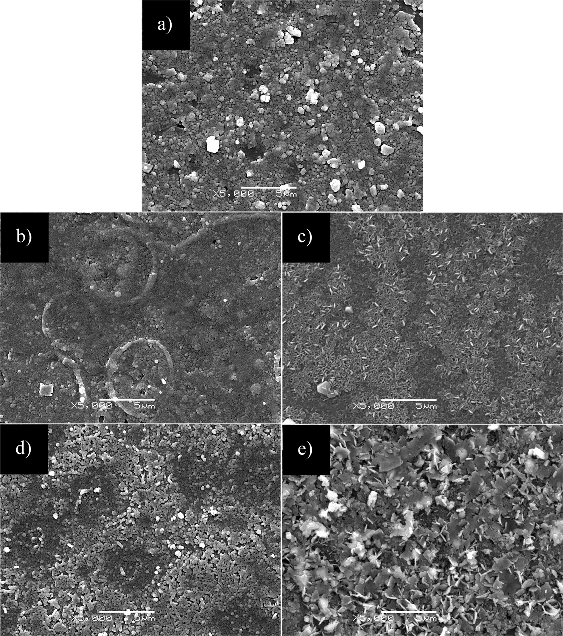
Morphology analysis of CuIn1-xGaxSe2
thin films
Fig. 5 shows the SEM images of CuIn0.8Ga0.2Se2,
CuIn0.6Ga0.4Se2, CuIn0.4Ga0.6Se2,
CuIn0.2Ga0.8Se2 and CuGaSe2 film
samples prepared at 220 °C for 20 h respectively. It can be seen that the
CuIn0.8Ga0.2Se2 and CuIn0.6Ga0.4Se2
films are dense and continuous and composed of spherical crystals with
diameters of about 0.2 to 0.3 μm, CuIn0.6Ga0.4Se2
film has a non-uniform particle size. The CuIn0.4Ga0.6Se2
film is composed of rod-like crystals with lengths of about 0.8 to 1.0 μm, and
its shape is similar to rod shape gathered together with crystal grains. The
CuIn0.2Ga0.8Se2 film consists of small rod-like
crystals with lengths of about 0.3 to 0.5 μm, and its length and size are
smaller than those of the CuIn0.4Ga0.6Se2
film. The CuGaSe2 film is composed of rod-like crystals with lengths
of about 0.8 to 1.0 μm and irregular sheet crystals.
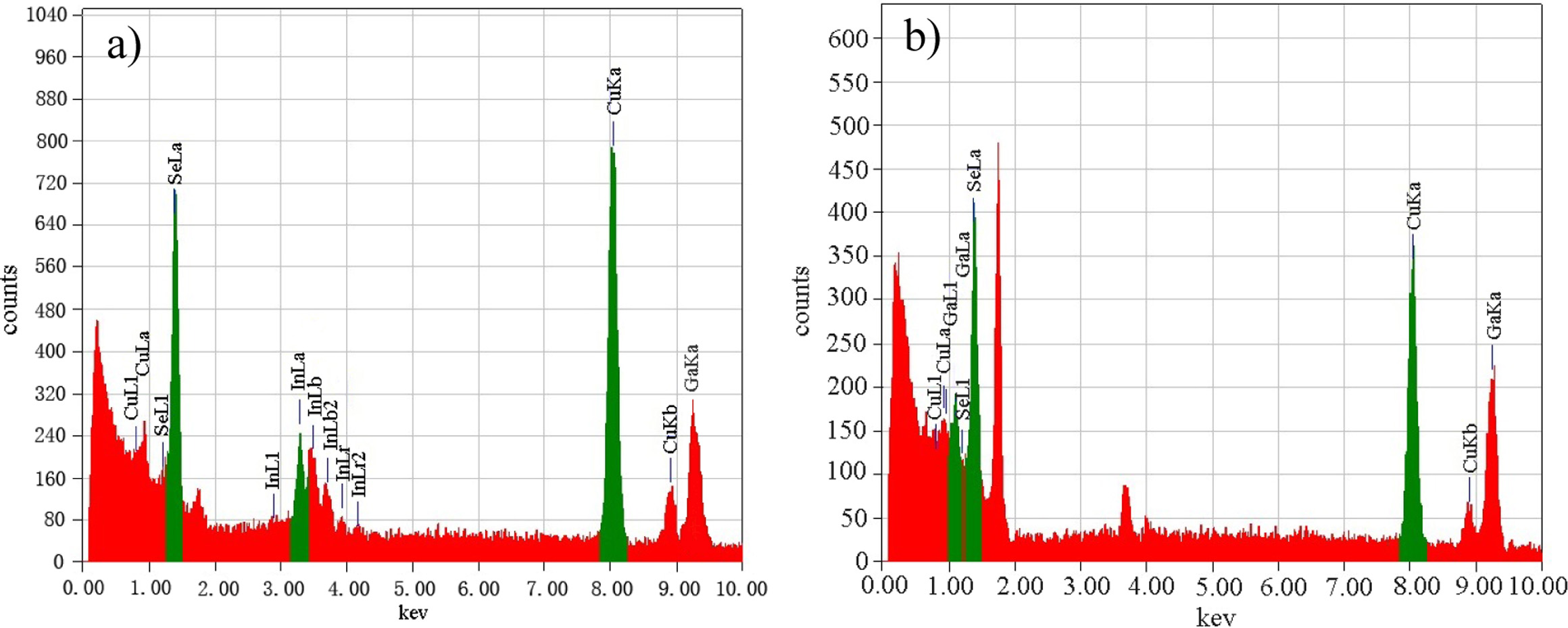
Composition
analysis of CuIn1-xGaxSe2 film by EDS
Fig. 6 shows the EDS spectrums of CuIn0.2Ga0.8Se2
film and CuGaSe2 film prepared by spin-coating and co-reduction
method. It can be seen from Fig. 6(a) that Cu, Se, In and Ga elements appear
from left to right, it confirmed
that the above four elements are contained in the product
film, although the element ratio is not necessarily stoichiometric. Fig. 6(b)
indicates that CuGaSe2 film sample consists of Cu, Se and Ga elements.
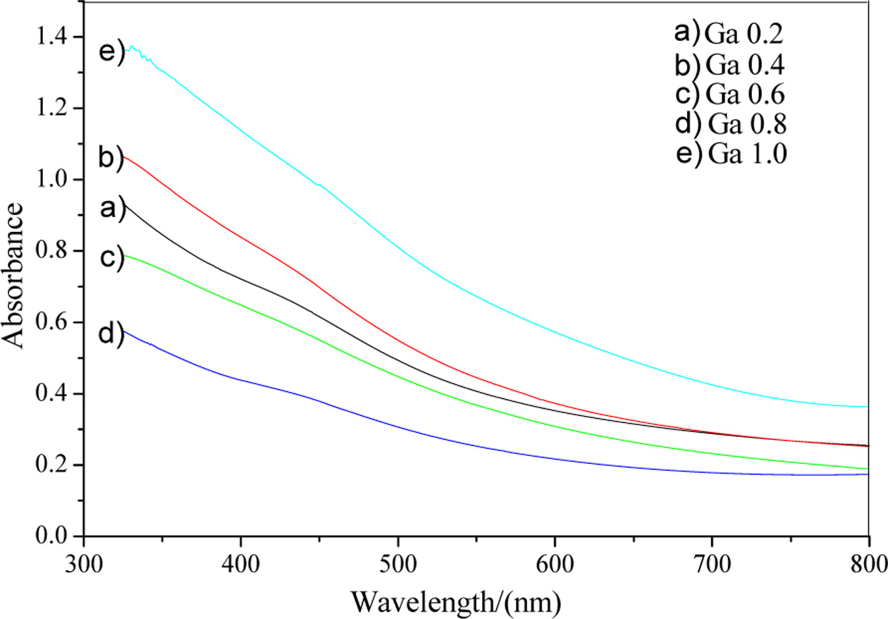
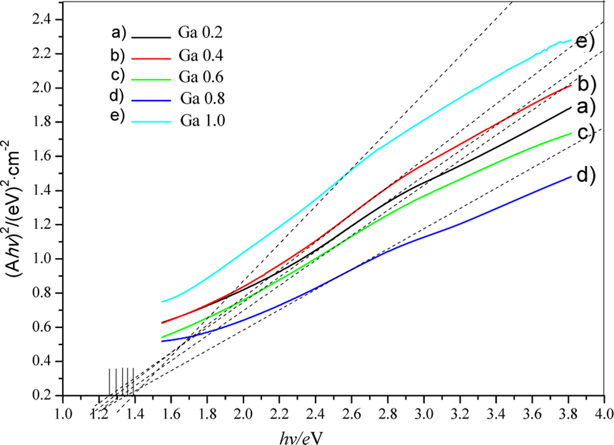
Estimation
of the band gaps of CuIn1-xGaxSe2 thin films
The absorption spectrums of the film samples were tested using
a UV-Vis method on a visible spectrophotometer. Fig. 7 shows
the absorbance of CuIn1-xGaxSe2 films with
different doping concentrations prepared at 220 °C for 20 h. The band gaps
of the film samples were then estimated by extrapolation as shown in Fig. 8. It
can be seen that the estimated band gaps of CuIn0.8Ga0.2Se2,
CuIn0.6Ga0.4Se2, CuIn0.4Ga0.6Se2,
CuIn0.2Ga0.8Se2 and CuGaSe2 films
are 1.25 eV, 1.3 eV, 1.33 eV, 1.38 eV and 1.4 eV, respectively.
|
Fig. 1 XRD patterns of CuIn1-xGaxSe2 prepared at 220 °C for different reaction time. (a) CuIn0.9Ga0.1Se2, (b) CuIn0.8Ga0.2Se2, (c) CuIn0.7Ga0.3Se2, (d) CuIn0.6Ga0.4Se2, e) CuIn0.5Ga0.5Se2, (f) CuIn0.4Ga0.6Se2, (j) CuIn0.3Ga0.7Se2, (h) CuIn0.2Ga0.8Se2, (i) CuIn0.1Ga0.9Se2, (j) CuGaSe2. |
|
Fig. 2 XRD patterns of CuIn1-xGaxSe2 reacted at different temperatures for 20 h. (a) CuIn0.9Ga0.1Se2, (b) CuIn0.8Ga0.2Se2, (c) CuIn0.7Ga0.3Se2, (d) CuIn0.6Ga0.4Se2, (e) CuIn0.5Ga0.5Se2, (f) CuIn0.4Ga0.6Se2, (j) CuIn0.3Ga0.7Se2, (h) CuIn0.2Ga0.8Se2, (i) CuIn0.1Ga0.9Se2. |
|
Fig. 3 XRD patterns of CuIn1-xGaxSe2 with different doping concentrations prepared at 220 °C for 20 h. |
|
Fig. 4 The resistivities of CuIn1-xGaxSe2 films with different doping concentrations prepared at 220 °C for 20 h. |
|
Fig. 5 SEM images of CuIn1-xGaxSe2 with different doping concentrations prepared at 220 °C for 20 h. (a) CuIn0.8Ga0.2Se2, (b) CuIn0.6Ga0.4Se2, (c) CuIn0.4Ga0.6Se2, (d) CuIn0.2Ga0.8Se2, (e) CuGaSe2. |
|
Fig. 6 EDS spectrums of CuIn0.2Ga0.8Se2 and CuIn0.2Ga0.8Se2 films reacted at 220 °C for 20 h. Target products: (a) CuIn0.2Ga0.8Se2, (b) CuGaSe2. |
|
Fig. 7 UV-Vis spectrums of CuIn1-xGaxSe2 with different doping concentrations at 220 °C for 20 h. |
|
Fig. 8 Estimation of band gaps of CuIn1-xGaxSe2 with different doping concentrations at 220 °C for 20 h. |
The CuIn1-xGaxSe2 films
were prepared by spin-coating and co-reduction method. It was
found by phase analysis that longer reaction time and higher reaction temperature
were beneficial to the sample crystallization, the
better experimental conditions for preparing CuIn1-xGaxSe2
films are at 220 °C for 20 h. With the increase of
doping concentration, the surface morphology of
CuIn1-xGaxSe2 films changed with a tendency
from spherical
crystals to rods. The effect of doping concentration
on the resistivity is not particularly obvious. As the doping concentration increases, the resistivity will increase slightly. When x=1, the resistivity
changes greatly, which may be due to
the poor continuity of the film. According to the absorbance of CuIn1-xGaxSe2
films, their estimated band gaps are 1.25 eV, 1.3 eV, 1.33 eV, 1.38 eV and 1.4
eV, respectively.
This work was financially
supported by the National Natural Science Foundation of China (No.51272140) and
the Innovation Team of the Co-Innovation Center for Green Building of Shandong
Province in Shandong Jianzhu University
- 1. R. Bouferra, G. Marín, S. Amhil, S. M. Wasim, and L. Essaleh, Physica B. 565 (2019) 14-17.
-

- 2. S.M. Chauhan, S.H. Chaki, M. P. Deshpande, J.P. Tailor, and A.J. Khimani, Mat. Sci. Semicon. Proc. 74 (2018) 329-335.
-
- 3. Y.J. Park, S.W. Kim, K. Sugimoto, T. Hasegawa, K. Tanima, K. Uematsu, K. Toda, and M. Sato, J. Ceram. Process. Res. 20[5] (2019) 460-463.
-
- 4. T. Kato, N. Kawaguchi, and T. Yanagida, J. Ceram. Process. Res. 20[5] (2019) 449-454.
-
- 5. H. Fukushima, D. Nakauchi, N. Kawaguchi, and T.Yanagida, J. Ceram. Process. Res. 20[3] (2019) 211-215.
-
- 6. T.T. Khan and S.C. Ur, J. Ceram. Process. Res. 19[4] (2018) 327-331.
- 7. A. Aissata and M. Fathib, J.P. Vilcotc, Energy Procedia 18 (2012) 197-204.
-
- 8. G. Yin and P. Manley, M. Schmid, Sol. Energy 163 (2018) 443-452.
-
- 9. Y.-S. Cheng, N.-F. Wang, Y.-Z. Tsai, J.-J. Lin, and M.-P. Houng, Appl. Surf. Sci. 396 (2017) 631-636.
-
- 10. C.-S. Chiou and H.-C. Peng, Sol. Energy 146 (2017) 436-442.
-
- 11. B. Noikaew and S. Chatraphorn, Surf. Coat. Tech. 307 (2016) 547-553.
-
- 12. Y.-F. Wu, H.-P. Hsu, and H.-I. Chen, J. Lumin. 142 (2013) 81-85.
-
- 13. M. Behr, M. Sharma, S. Sprague, N. Shinkel, J. Kerbleski, C. Alvey, S. Rozeveld, T. Hasan, C. Wintland, M. Mushrush, and A. Wall, Thin Solid Films 665 (2018) 36-45.
-
- 14. S. Mandati, B.V.Sarada, S.R. Dey, and S.V. Joshi, Mater. Lett. 118 (2014) 158-160.
-
- 15. H.T. Xue, F.L. Tang, F.Z. Zhang, W.J. Lu, and Y.D. Feng, Mater. Lett. 164 (2016) 169-171.
-
- 16. S. Sunkoju, S. Schujman, D. Dixit, A. Diebold, J. Li, R. Collins, and P. Haldar, Thin Solid Films 606 (2016) 113-119.
-
- 17. A. Khanaki, H. Abdizadeh, and M.R. Golobostanfard, Mat. Sci. Semicon. Proc. 16 (2013) 1397-1404.
-
- 18. A.B. Marai, J.B. Belgacem, Z.B. Ayadi, K. Djessas, and S. Alaya, J. Alloy Compd. 658 (2016) 961-966.
-
- 19. R.-W. You, K.K. Lew, and Y.-P. Fu, Mater. Res. Bull. 96 (2017) 183-187.
-
- 20. K.G. Liu, Y. Xu, Q.L. Sun, H.P. Li, and H.Y. Wu, Results in Physics, 12 (2019) 766-770.
-
 This Article
-
2020; 21(2): 226-232
Published on Apr 30, 2020
- 10.36410/jcpr.2020.21.2.226
- Received on Nov 23, 2019
- Revised on Jan 13, 2020
- Accepted on Jan 17, 2020
Services
- Abstract
introduction
experimental
preparation and characterization of cuin1-xgaxse2films
summary
- Acknowledgements
- References
- Full Text PDF
Shared
Correspondence to
- Jing Li, Kegao Liu
-
School of Materials Science and Engineering, Co-Innovation Center for Green Building of Shandong Province, Shandong Jianzhu University, Fengming Road, Jinan 250101, China
Tel : +86-15610183153 - E-mail: liukg163@163.com
Clean-Energy Research Institute(CRI), Hanyang University, 222, Wangsimni-ro, Seongdong-gu, Seoul, 04763, Korea
E-mail: jcpr@hanyang.ac.kr