


- Synthesis of three-dimensional cactus-shaped SnO2 crystals via thermal evaporation of Sn
Min-Sung Kim*
Department of Information & Communications Engineering, Tongmyong University, Busan 48520, Korea
SnO2 crystals were
fabricated by thermal evaporation of Sn powder at 900°C in an oxygen atmosphere
without any catalyst. The growth time was varied in a range of 1 ~ 3
h in order to investigate the morphological change during growth of the
crystals. Scanning electron microscopy, X-ray diffractometry, energy dispersive
X-ray spectroscopy, and cathodoluminescence spectroscopy were used to
characterize the morphologies, crystal structures, and luminescence properties
of the SnO2 crystals. X-ray diffraction analysis showed that the SnO2
crystals had a rutile crystallographic structure. When the growth time was 1 h,
SnO2 microrods with a rough surface were observed. With an increase
of the growth time to 2 h, many nanowires on the SnO2 microrods such
that microrod-nanowire assembly had a cactus-like appearance. When the growth
time was further increased to 3 h, micro/nanowires were observed. A strong
visible emission peak centered at about 480 nm was observed in the room
temperature cathodoluminescence spectra of all the samples.
Keywords: Tin powder, Thermal evaporation, Tin oxide micro-rods, Cactus shape
Metal-oxide micro/nanocrystals recently have attracted
attention due to their novel properties and potential applications in
electronics and optoelectronics. Micro/nanocrystals of functional metal oxides
have been synthesized because they lend the possibility of
fabricating smart devices by exploiting their novel electrical,
optical, and magnetic properties. Among functional metal oxides, SnO2
with a wide band gap of 3.6 eV is one of the most important metal oxides with
many applications. It has been widely employed in various fields of solar
cells, light emitting diodes, transparent electrodes, transistors, photovoltaic
cells, lithium ion battery electrodes, and gas sensors.
In particular, SnO2 is an outstanding material
for gas sensors due to its advantages including high sensitivity, fast response
and recovery time, chemical and thermal stability, and high mechanical
strength. Thus, SnO2 is widely used as gas sensing material to
detect extremely hazardous gases. The sensing mechanism of SnO2 is
based on the change in the conductivity which is caused by the reaction between
the oxygen and the detected gas on the surface of the SnO2 material.
Hence, the surface area has a strong impact on the sensing performance.
The sensing performance is improved with an increase in the surface area of
sensing material. In general, micro/nanocrystals have large surface area, which results in the
enhancement of the sensing performance [1-5]. Accordingly, consideration effort
has been devoted to the synthesis of SnO2
micro/nanocrystals.
So far, diverse morphologies of SnO2 micro/nano-crystals
such as wires [6], belts [7], rods [8], and tubes [9] have been
synthesized. Especially, a three-dimensional (3D)
hierarchical morphology such as flower-like and dendritic shapes is thought to
be most effective for improving the sensing performance of gas sensors due to
the high surface area relative to volume [10]. In addition, 3D morphology is
favorable for the diffusion of gas molecules, which is important for improving
the sensitivity and response time of gas sensors. Thus, the facile synthesis of
SnO2 crystals with a 3D morphology is of considerable interest.
SnO2 micro/nanocrystals with a 3D morphology
have been mainly synthesized using wet chemical methods including hydrothermal
and sol-gel methods [11-15]. The wet chemical processes are carried out at
relatively low temperatures. The drawback of the low-temperature processes
is the poor crystallinity of micro/nanocrystals. Therefore,
dry process methods have received increasing attention in
synthesizing 3D SnO2 micro/nanocrystals. The dry
methods include thermal evaporation, chemical vapor
deposition, and pulsed laser deposition. Among them, thermal evaporation is a
relatively simple and low cost technique. There are few
reports on the synthesis of 3D SnO2 micro/nanocrystals using thermal
evaporation [16, 17]. In the reports, the 3D SnO2
micro/nanocrystals were grown via vapor-liquid-solid (VLS) mechanism.
Metal catalysts are essential in the VLS mechanism. But the catalysts can
create contamination in the micro/nanocrystals. Thus, it is
worthwhile to develop a catalyst-free thermal evaporation process
for synthesizing 3D SnO2 micro/nanocrystals.
In this paper, the facile synthesis of 3D cacti-like SnO2
crystals via thermal evaporation of Sn powder without using catalyst is
reported.
Sn powder with a purity of 99.99% was used as the source
material. The alumina crucibles with the Sn powder were placed in the middle of
a horizontal quartz tube furnace. The quartz tube was evacuated to a pressure
of 1 × 10⁻¹
Torr by using a mechanical pump. Then oxygen was introduced into the quartz
tube until the pressure reached 100 Torr. The pressure was maintained at 100
Torr throughout the experiment. The temperature was set to 900 °C and the
growth time was varied in a range of 1 ~ 3 h to investigate the
effect of growth duration on the morphology of the products. The
furnace was subsequently cooled to room temperature. The products
in the crucibles were collected for characterization.
X-ray diffraction (XRD) patterns were obtained to
investigate the crystalline structure of the as-synthesized products. Field
emission scanning electron microscopy (FESEM) was used to
investigate the crystalline structure of the as-synthesized
products. An energy dispersive X-ray (EDX) spectroscope was employed to study
the components of the products. The cathodoluminescence (CL) measurement was
carried out at room temperature.
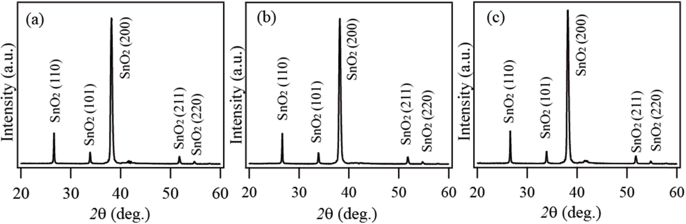
Fig. 1 shows the XRD spectra of the products synthesized
by thermal evaporation of Sn powder at 900 °C
in an O2 ambient for 1 h, 2 h, and 3 h, respectively.
XRD spectra reveal similar XRD peak patterns for all the products. The
diffraction peaks are identical to the tetragonal rutile structure of SnO2
with lattice constants of a = b = 0.473 nm and
c = 0.318 nm, indicating that all the products are SnO2 with
a rutile structure. No peaks were detected for other crystalline phase of
impurities.
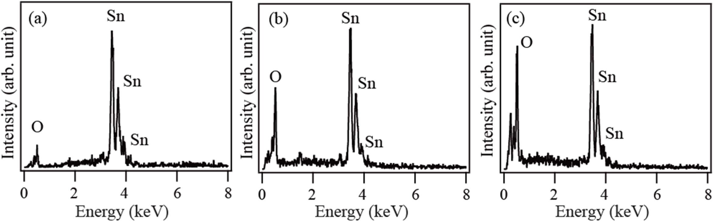
Fig. 2 shows the EDX spectra of the products synthesized
by thermal evaporation of Sn powder at 900 °C in an O2 ambient
for 1 h, 2 h, and 3 h, respectively. Only Sn and O are detected in the spectra,
which confirms that the products are high purity SnO2.
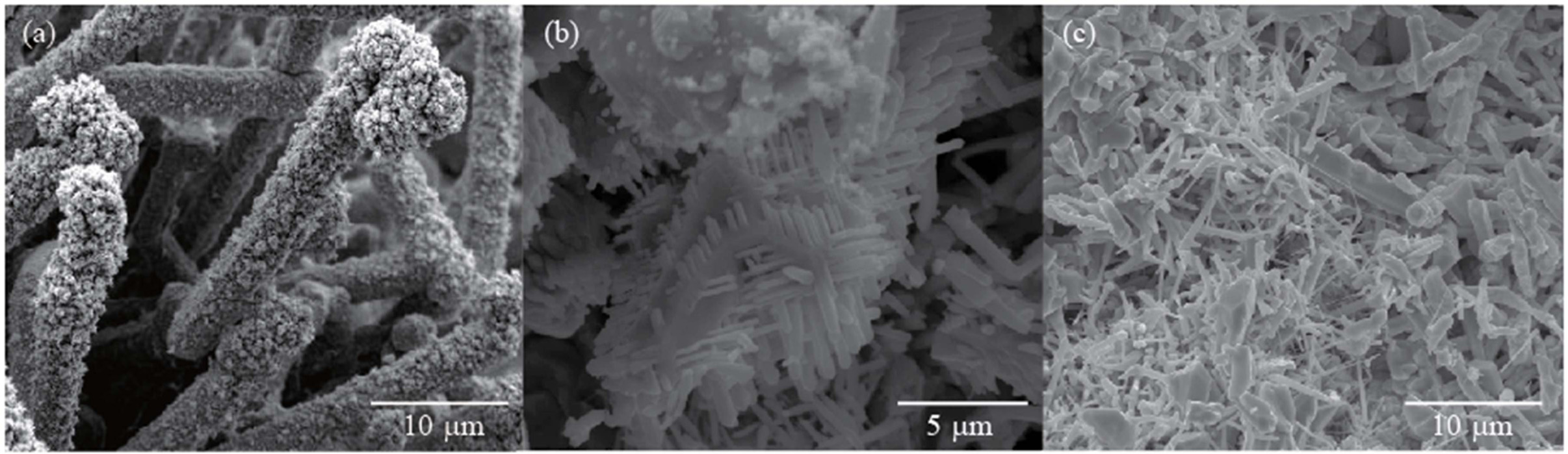
Fig. 3 shows SEM images of the SnO2 crystals
synthesized by thermal evaporation of Sn powder at 900 °C
in an O2 ambient for 1 h, 2 h, and 3 h, respectively.
When the growth time was 1 h, SnO2 microrods with a rough
surface were observed. The SnO2 microrods have
an average diameter of 4 μm and lengths of several tens of
micrometers. SnO2 micro/nanowires with a rough
surface have been observed in products synthesized through thermal evaporation
of Sn under a vacuum condition [18]. Upon increasing the growth time to 2 h,
the SEM image exhibits SnO2 microrods on which nanowires with high
density are grown. The SnO2 microrod consists of a main micro-sized
stem and numerous nanowires on the stem, which resembles a cactus-like
structure. The nanowires are grown on the rough surface
of the main stem. The main stems are 0.25 ~ 1 μm
in diameter and 7 ~ 15 μm in length, respectively.
The diameter and the length of the nanowires are 50 ~ 250 nm and
0.5 ~ 1.5 μm, respectively. Secondary branched nanowires as well as
primary branched nanowires are observed in the SEM images. The branched
nanowires have uniform diameter along the growth direction, which indicates
that the growth conditions remained constant during the growth. The secondary
branched nanowires were grown in a perfectly perpendicular direction to the
side of the main stem.
The growth mechanism of the cactus-like SnO2 microrods
with branched nanowires is posited as follows. Initially,
Sn powder is vaporized into Sn vapor. The Sn vapor reacts with the oxygen in
the atmosphere to form SnO2 nuclei. The nuclei grow along the
preferential direction, leading to the formation of main stems. The size of the
main stems increases with the growth time. Secondary nucleation and growth
occur on the main stems, which are sufficiently large to promote
secondary nucleation on their surfaces. The secondary nucleation
leads to the growth of primary branched nanowires on the main stems. The same
growth process is repeated on the primary branched nanowires, resulting in the
formation of secondary branched nanowires. The rough surface of the main stems would
favor secondary nucleation. On the other
hand, in the present experiment, the
growth of main stems and branched nanowires is considered to proceed via a vapor-solid (VS) mechanism because no catalysts were used and no catalyst
droplets were found at the tips of the nanowires. There are two growth mechanisms in the growth of the
one-dimensional nanowires and
nanorods. One is vapor-solid (VS) mechanism and the other is vapor-liquid-solid
(VLS) mechanism. In the VLS mechanism, metal catalyst is required to direct the
crystal growth on to specific orientation. The metal catalyst forms liquid
droplets and adsorbs vapor components
at the growth temperature. When the
liquid droplets become supersaturated with the absorbed components, the
components start to precipitate and continued precipitation results in the
growth of nanowires. Therefore, catalyst particles are typically observed at
the tips of nanowires grown via VLS mechanism [19, 20]. In this work, no
catalyst particles were observed at the tips of the branched nanowires,
indicating that the nanowires were grown via VS mechanism.
After growth time of 3 h, SnO2 microrods with
branched nanowires were not observed and micro/nanowires were found. It is
known that SnO2 is an oxide that becomes unstable above 500 °C
[21]. Thus, in the present work, the SnO2 microrods would decompose
into Sn and oxygen because of prolonged growth time and then Sn vapor would
react with oxygen to form SnO2 nanowires.
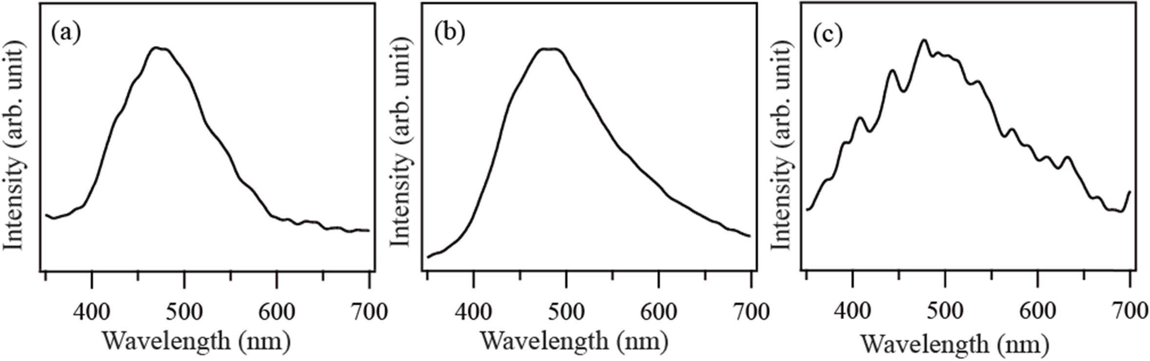
Figs. 4(a), (b), and (c) show the CL spectra of the SnO2
crystals synthesized by thermal evaporation of Sn powder at
900 °C in an O2 ambient for 1 h, 2 h, and 3 h,
respectively. A broad visible emission with a maximum at 480 nm is dominantly
observed in the CL spectra. The broad visible emission has been observed from
SnO2 crystals at room temperature [22, 23]. The visible
luminescence is known to be associated with oxygen vacancies. Luo et al
reported that the emission peak at 480 nm also originated from surface oxygen
vacancies [24]. Because SnO2 is an n-type semiconductor, the
presence of oxygen vacancies is related to the n-type semiconducting property.
Accordingly, it is suggested that the visible emission observed in the present
experiment can be attributed to oxygen-related defects.
|
Fig. 1 XRD spectra of the products synthesized at 900°C for (a) 1 h, (b) 2 h and (c) 3 h, respectively. |
|
Fig. 2 EDX spectra of the products synthesized at 900°C for (a) 1 h, (b) 2 h and (c) 3 h, respectively. |
|
Fig. 3 SEM images of the products synthesized at 900°C for (a) 1 h, (b) 2 h and (c) 3 h, respectively. |
|
Fig. 4 Room temperature CL spectra of the products synthesized at 900°C for (a) 1 h, (b) 2 h and (c) 3 h, respectively. |
SnO2 micro/nanocrystals with a tetragonal
rutile structure could be formed via thermal evaporation of Sn powder
in oxygen ambient at 100 Torr. The morphology of SnO2
micro/nanocrystals was significantly affected by an
increase in growth time. As growth time increased, the
morphology of the SnO2 micro/nanocrystals changed
from microrods to cactus-like microrods on which numerous nanowires were grown.
The cactus-like microrods consisted of main stems and many branched nanowires.
Secondary branched nanowires as well as primary branched nanowires were
observed on the microrods. It is considered that the 3D cactus-like
hierarchical SnO2 crystals were grown via VS growth. In the room
temperature CL spectra, a strong visible emission at 480 nm was observed, and
this might be attributable to oxygen vacancies. The unique 3D
cactus-like SnO2 crystals have high accessible
surface area and considerable inter-nanowire space, which can provide more
active sites. Thus the cactus-like crystals can be used as a potential material
for highly efficient gas sensors, catalysts, dye-sensitized solar cells, and
Li-ion batteries.
This Research was supported by the Tongmyong University
Research Grants 2019.
- 1. S. Supothina, M. Suwan, and A. Wisitsoraat, J. Ceram. Process. Res. 14 (2013) 226-229.
- 2. H. Yu, T. Yang, Z. Wang, Z. Li, B. Xiao, Q. Zhao, and M. Zhang, J. Alloy. Compd. 724 (2017) 121-129.
-

- 3. R. Zhao, Z. Wang, Y. Yang, X. Xing, T. Zou, Z. Wang, and Y. Wang, J. Phys. Chem. Solids 120 (2018) 173-182.
-
- 4. X. Lian, Y. Li, J. Zhu, Y. Zou, X. Liu, D. An, and Q. Wang, Curr. Appl. Phys. 19 (2019) 849-855.
-
- 5. T. Li, W. Zeng, H. Long, and Z. Wang, Sens. Actuat. B-Chem. 231 (2016) 120-128.
-
- 6. J.M. Jeong, Y.J. Kwon, H.Y. Cho, H.G. Na, and H.W. Kim, J. Ceram. Process. Res. 15 (2014) 428-432.
- 7. S.H. Sun, G.W. Meng, Y.W. Wang, T. Gao, M.G. Zhang, Y.T. Tian, X.S. Peng, and L.D. Zhang, Appl. Phys. A. 76 (2003) 287-289.
-
- 8. H.W. Kim, J.W. Lee, S.H. Shim, and C. Lee, J. Korean Phys. Soc. 51 (2007) 198-203.
-
- 9. W. Jin, Z. Tian, L. Lin, D. Jiatao, Z. Gang, Z. Pei, J. Yong, J. Zhifeng, and S. Xiaosong, Mater. Lett. 180 (2016) 38-41.
-
- 10. H. Wang, and A.L. Rogach, Chem. Mater. 26 (2014) 123-133.
-
- 11. J.R. Hunag, K. Yu, C.P. Gu, M.H. Zhai, Y.J. Wu, M. Yang, and J.H. Liu, Sens. Actuat. B-Chem. 147[2] (2010) 467-474.
-
- 12. H. Wang, Q.Q. Liang, W.J. Wang, Y.R. An, J.H. Li, and L. Guio, Cryst. Growth Des. 11 (2011) 2942-2947.
-
- 13. R. Yang, Y.G. Gu, Y.Q. Li, J. Zheng, and X.G. Li, Acta Mater. 58 (2010) 866-874.
-
- 14. Y.L. Wang, M. Guo, M. Zhang, and X.D. Wang, Scripta Mater. 61 (2009) 234-236.
-
- 15. Q, Wang, L.S. Zhang, J.F. Wu, W.D. Wang, W.G. Song, and W. Wang, J. Phys. Chem. C 114 (2010) 22671-22676.
-
- 16. Z. Guo, X. Chen, W.H. Xu, J. Li, G.M. Yang, M.Q. Li, J.H. Liu, and X.J. Huang, Mater. Today 14 (2011) 42-49.
-
- 17. S.H. Mohamed, J. Alloy. Compd. 510 (2012) 119-124.
-
- 18. N.M. Shaalan, T. Yamazaki, and T. Kikuta, Sens. Actuat. B-Chem. 153[1] (2011) 11-16.
-
- 19. W.I. Park, J. Ceram. Process. Res.9 (2008) 666-671.
- 20. R.S. Wagner, and W.C. Ellis, Appl. Phys. Lett. 4 (1964) 89-90.
-
- 21. D. Zhang, X. Li, F. Wan, C.J. Thong, M.A. Rindfleisch, M.J. Tomsic, M.D. Sumption, and E.W. Collings, Mater. Sci. Eng. 279 (2017) 012025.
-
- 22. S.H. Luo, Q. Wan, W.L. Liu, M. Zhang, Z.T. Song, C.L. Lin, and P.K. Chu, Prog. Solid State Chem. 33 (2005) 287-292.
-
- 23. S. Luo, J. Fan, W. Liu, M. Zhang, Z. Song, C. Lin, X. Wu, and Paul K. Chu, Nanotechnology 17 (2006) 1695-1699.
-
- 24. S. Luo, P.K. Chu, W. Liu, M. Zhang, and C. Lin, Appl. Phys. Lett. 88 (2006) 183112.
-
 This Article
-
2020; 21(1): 119-122
Published on Feb 28, 2020
- 10.36410/jcpr.2020.21.1.119
- Received on Nov 14, 2019
- Revised on Dec 15, 2019
- Accepted on Dec 24, 2019
Services
- Abstract
introduction
experimental
results and discussion
conclusion
- Acknowledgements
- References
- Full Text PDF
Shared
Correspondence to
- Min-Sung Kim
-
Department of Information & Communications Engineering, Tongmyong University, Busan 48520, Korea
Tel : +82-51-629-1148 Fax: +82-51-629-1148 - E-mail: minsung@tu.ac.kr
Clean-Energy Research Institute(CRI), Hanyang University, 222, Wangsimni-ro, Seongdong-gu, Seoul, 04763, Korea
E-mail: jcpr@hanyang.ac.kr