


- Influence of surface roughness on the efficiency of a flexible organic solar cell
Se Hoon Kima, Deuk Yong Leeb and Young-Jei Oha,c,*
aOpto-electronic Materials & Devices Research Center, Korea Institute of Science and Technology, Seoul 02792, Korea
bDepartment of Biomedical Engineering, Daelim University, Anyang 13916, Korea
cDepartment of Nano Material Science and Engineering, Korea University of Science and Technology, Daejeon 34113, Korea
Organic solar cells (OSCs)
without an over-coating layer, consisting of a silver nanowire (AgNW)
transparent electrode, a poly(3,4-ethylenedioxythiphene):poly
(styrenesulfonate) (PEDOT:PSS) layer, a poly(3-hexylthiophene-2,5-diyl):the
[6,6]-phenyl C61 butyric acid methyl ester (P3HT:PCBM) active layer, a LiF/Al
electron collecting, and a top electrode, were successfully fabricated in order
to investigate the effect of surface roughness on the efficiency of OSCs. The
AgNW transparent electrode on acryl resin coated polyethylene terephthalate
(PET) film was prepared through the filtration/transfer method. Sheet
resistance of 30 Ω-1 and surface roughness of 10.5 nm were detected.
After coating the PEDOT:PSS hole transfer layer and the P3HT:PCBM active layer
at 1000 rpm on the AgNW/PET transparent electrode, the surface roughness was
reduced dramatically. However, open circuit voltage, short circuit current
density, fill factor, and power conversion efficiency decreased as the coating
speed was raised during the formation of the PEDOT:PSS layer and the P3HT:PCBM
active layer due to the deterioration of the surface roughness. The surface
roughness was determined to be crucial for the output performance of OSCs.
Keywords: silver nanowire (AgNW), filtration/transfer method, spin coating, surface roughness, organic solar cell (OSC)
Although indium tin oxide (ITO) is widely used as a transparent
electrode material due to its excellent electrical conductivity
and transmittance of 85% or more in the visible light region, its high price
and a shortage of indium resources limit its widespread use [1-14]. In
addition, when the ITO film on a flexible substrate is bent, it becomes cracked
or broken [4, 5]. Its brittleness and high surface resistance make it difficult
to use in flexible electronic devices. An increased demand for flexible
electronic devices has fueled the development and
introduction of new transparent conducting materials such
as conducting polymers, carbon nanotubes (CNTs), graphene,
highly conductive poly(3,4-ethylenedioxythi-phene):poly
(styrenesulfonate) (PEDOT:PSS), and metal nanowire as
alternatives to ITO [1-9]. The transparent electrode material is used for
photo-electronic devices such as organic light-emitting diodes and organic
solar cells (OSCs). Solar cell technology should provide a safe, clean, and
most affordable potential energy source among renewable energy technologies
such as dye-sensitized solar cells [15-18]. The OSC has several advantages,
which include low cost, renewability, and energy
harvest due to high power conversion efficiency [4].
Among the alternatives, metal nanowires possessing
excellent transmittance, sheet resistance, and flexibility can be made into a
large area at a low cost compared to organic conducting polymers [5]. In this
work, flexible OSCs are fabricated using silver nanowires (AgNWs) as the transparent electrode on the substrate. AgNWs have been used as ITO in OSCs due to
their excellent conductivity, transmittance, and flexibility. The
disadvantages of AgNWs, such as low adhesion force on the substrate and low
resistance to corrosion, can be overcome by embedding AgNWs strongly in a polymer
surface [1]. The performance of the OSCs employing AgNWs is then evaluated as a
function of surface roughness.
To prepare an AgNW dispersion solution suitable for the
spraying method and filtration/transfer method, isopropyl alcohol, ethylene
glycol, ethylene glycol monoethyl ether and distilled water were used. The AgNW
dispersion solution was modified by adding a binder
(hydroxy propylmethyl cellulose) and a dispersant (Zonyl
FSO-100, DuPont) to prevent aggregation of the dispersed AgNW during drying
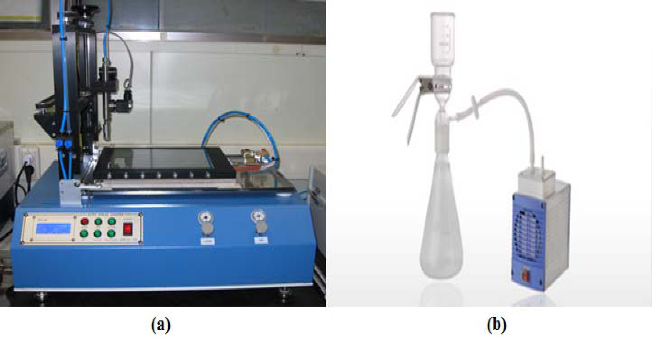
[8]. The bottom of the spray coating equipment, as shown in Fig. 1(a), was
heated to 80 oC. Then, the substrate was placed on the heated
bottom surface and it was fixed using a vacuum. The dispersed AgNW was placed
in a storage container for extrusion of the spray equipment. The liquid was
subjected to an extrusion pressure of 0.01 MPa and an air extrusion pressure of
0.01 MPa. The X and Y axis movement speed was 20 mm/sec and 2 mm/sec,
respectively. The transparent electrode was fabricated by spray-coating the
AgNW on the substrate.
The AgNW dispersed solution, which was used for the
filtration/transfer method (Fig. 1(b)), was poured into a Teflon filter paper
using a vacuum pump to leave only AgNWs on the filter paper. The substrate and
the AgNW remaining on filter paper were placed on the heated laminator at
120 oC and then pressed for 5 min at 0.1 kgf/cm2
to form a transparent electrode.
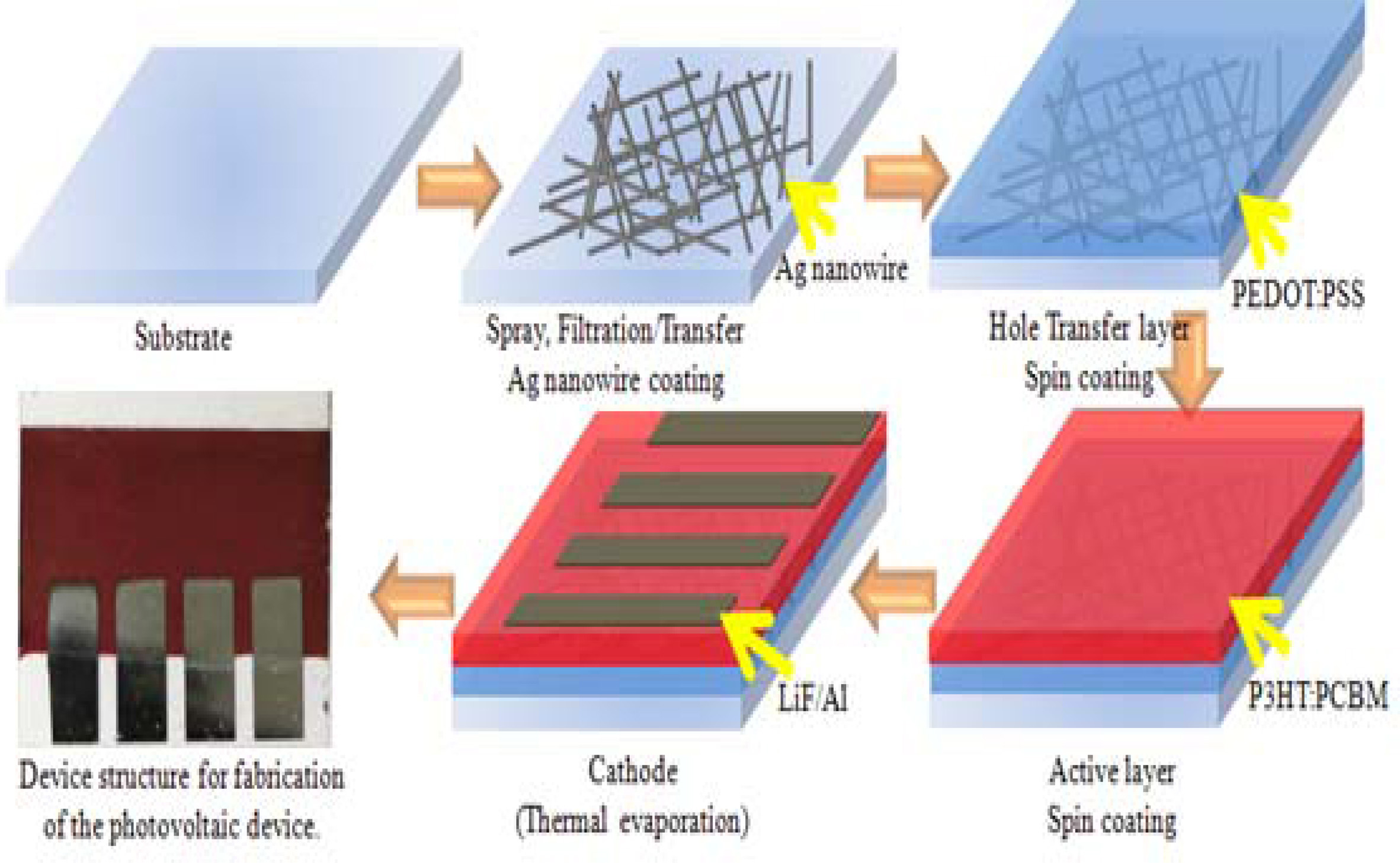
The device, as depicted in Fig. 2, consists of an AgNW
transparent electrode, a PEDOT:PSS as the hole collecting layer, a
poly(3-hexylthiophene-2,5-diyl):the [6,6]-phenyl C61 butyric acid methyl ester
(P3HT:PCBM) active layer, and a LiF/Al electron collecting and top electrode
[8]. Prior to spin-coating, the AgNW transparent electrode was UV treated for
15 min for better coating. A PEDOT:PSS bilayer (CleviosTM
PH 1000 and Al 4083, respectively) was spin-coated on the AgNW transparent
electrode as a hole transfer layer. The PEDOT:PSS was mixed with methanol at a
1: 1 volume ratio and this solution was spun at various speeds
in the range of 1,000 rpm, 2,000 rpm, 3,000 rpm to 4000 rpm
for 45 s, respectively, and subsequently dried on a hot plate for 30 min at
110 oC.
P3HT and PCBM (1:0.6 weight ratio) were melted in 1 mL of
chlorobenzene as an electron transport layer. The mixture was spin-coated at
1,000 rpm, 2,000 rpm, and 3000 rpm, respectively, after which it was dried on a
hot plate for 10 min at 150 oC. Finally, the LiF/Al electron-collecting
top electrode was subjected to thermal evaporation
to fabricate the final OSCs. The thickness of LiF and Al were 6 Å and 100 nm,
respectively.
|
Fig. 1 Photographs of (a) spray coater and (b) filtration apparatus. |
|
Fig. 2 Fabrication procedure of the OSCs. |
A dispersion solution of AgNW suitable for the spray method
and the filtration/transfer method was examined because the
electrical and optical properties were measured differently due to the
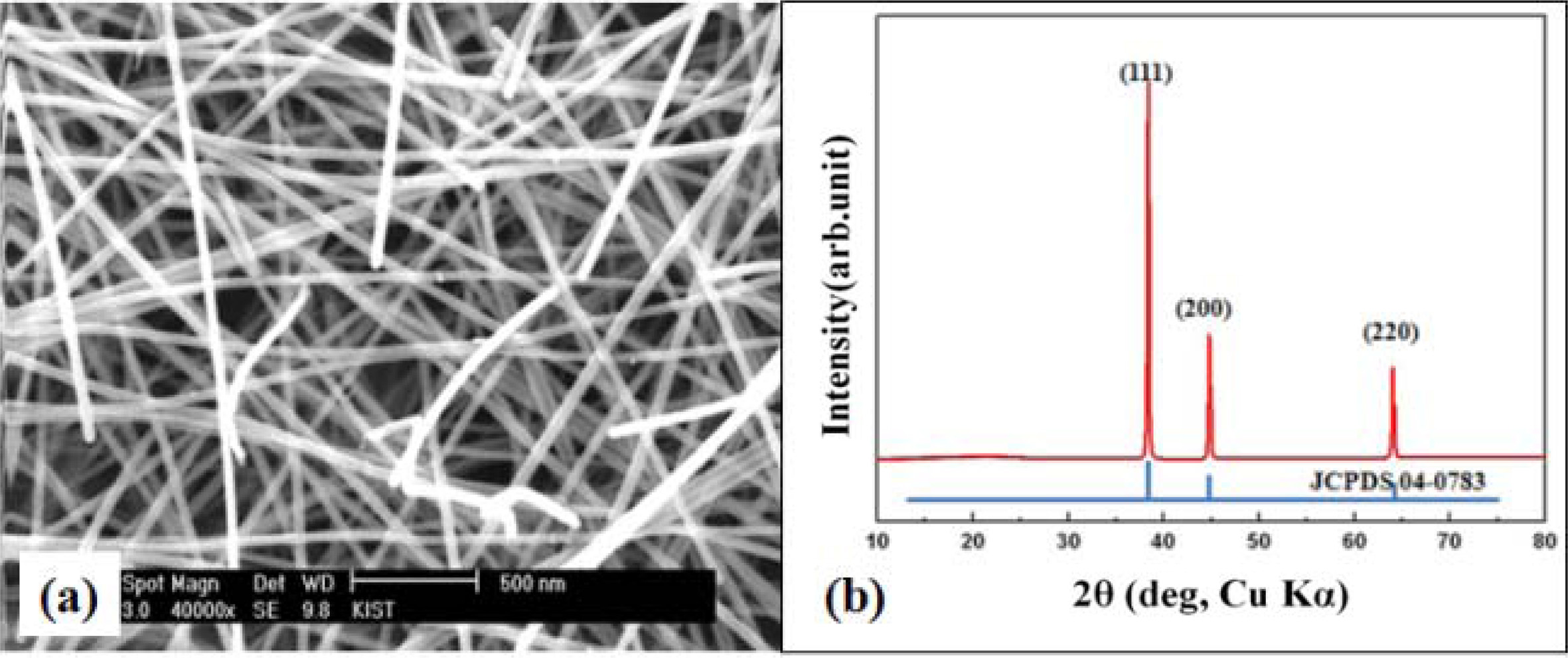
agglomeration between the AgNWs. SEM images in Fig. 3(a) show high linearity
and no cohesion between the AgNWs, which is suitable for the fabrication of
transparent electrodes [8]. XRD results revealed that the peaks in the AgNW
were consistent with (111), (200), and (220) planes from the standard powder
pattern of Ag (JCPDS-04-0783), as shown in Fig. 3(b). The crystal structure of
AgNWs was a face-centered cubic structure.
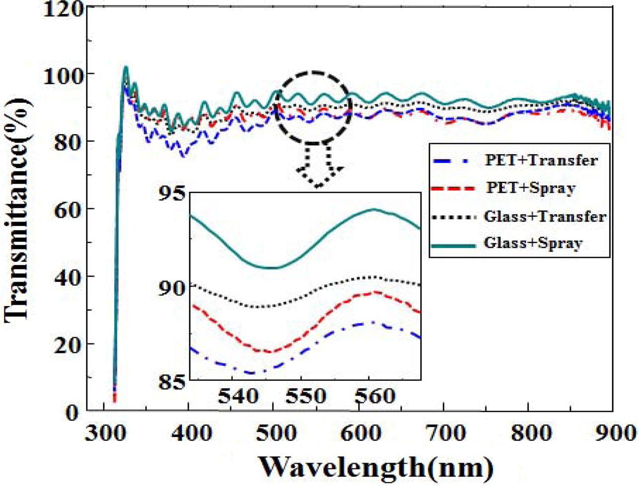
Transmittance of AgNW electrode on glass and PET
substrates is shown in Fig. 4. The transmittance of the transparent electrode
fabricated through the transfer method and the spray coating method on the PET
film coated with acryl resin was 85% and 87%, respectively. The transmittance
of the electrode prepared by the transfer method and the spray coating method
on the glass substrate was 90% and 93%, respectively. The transmittance of the
AgNW transparent electrodes was always higher than 85%, regardless of the
substrate type and the coating method. Conventional transparent electrodes
using ITO had a high transmittance of 85% in the visible light region and a low
sheet resistance (30 Ω-1)
[4]. The AgNW transparent electrode was highly suitable for an alternative
transparent electrode of ITO.
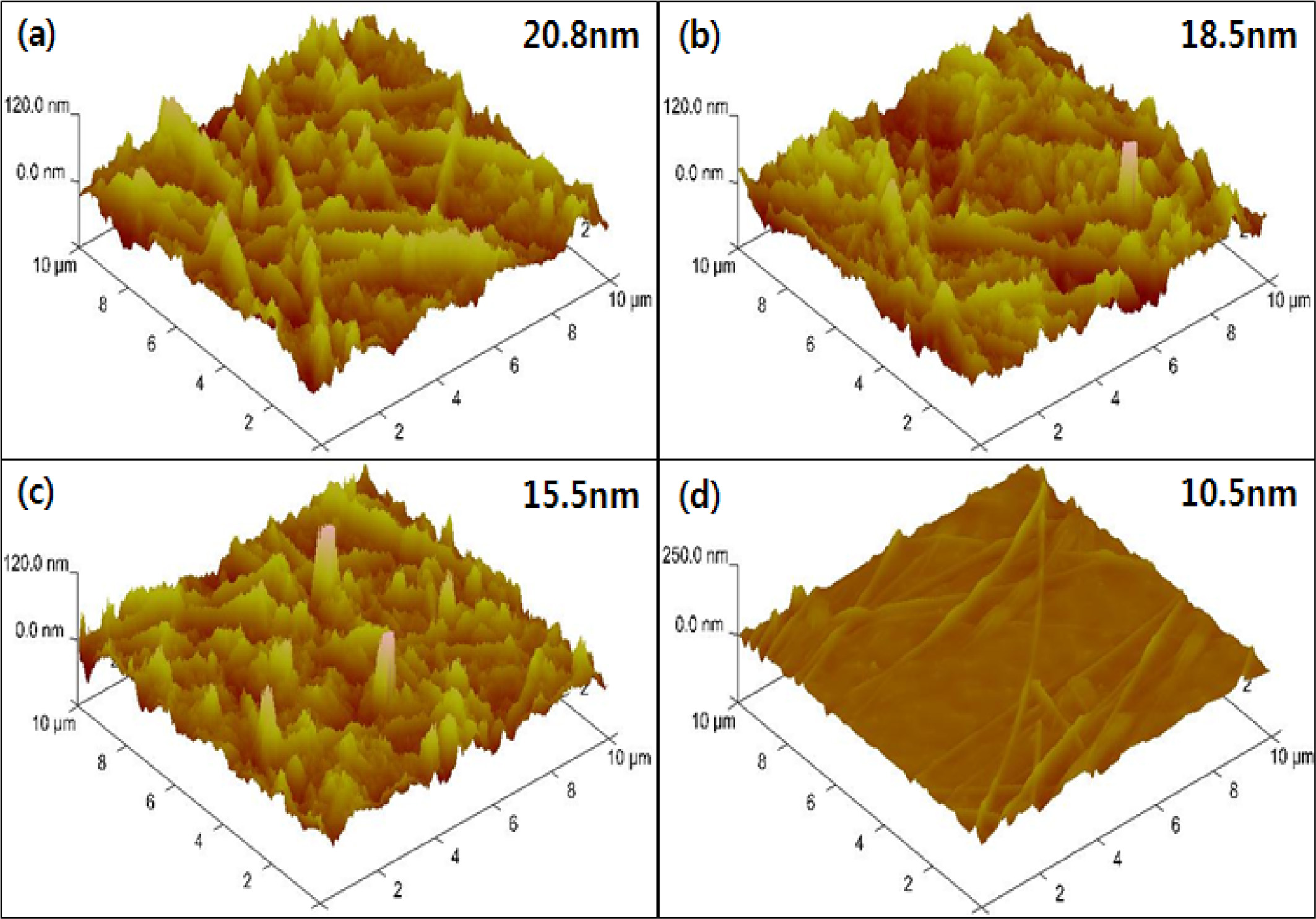
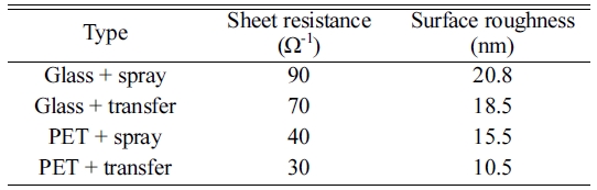
Sheet resistance and surface roughness are summarized
in Table 1. The surface roughness of a transparent electrode on acryl resin
coated PET film, as displayed in Figs. 5 and 6, was slightly improved from 15.5
nm to 10.5 nm when the transparent electrode was prepared using
the transfer method rather than the spray coating method. It was reported that
the enhanced surface roughness of the AgNW mesh film could prevent an undesired
leakage current path, leading to an improvement in device
yield and reproducibility [9]. In addition, the acrylic resin buffer layer
significantly strengthened the adhesion of AgNW mesh to the PET substrate. The
roughness of the transparent electrode was dramatically deteriorated – from
10.5 nm to 18.5 nm – when it was coated on glass through the transfer method.
The transfer method was found to be a better method than the spray coating
method regardless of the substrate type. The sheet resistance of a transparent
electrode on acryl resin coated PET film prepared through the transfer method
and spray coating method was 30 Ω-1
and 40 Ω-1,
respectively. The sheet resistance rose significantly to 90 Ω-1
when both the spray coating method and the glass substrate were employed.
Improved surface roughness was essential for efficient flexible OSC due to low
sheet resistance. In the present study, the AgNW transparent electrode on acryl
resin coated PET film prepared through the transfer method was investigated.
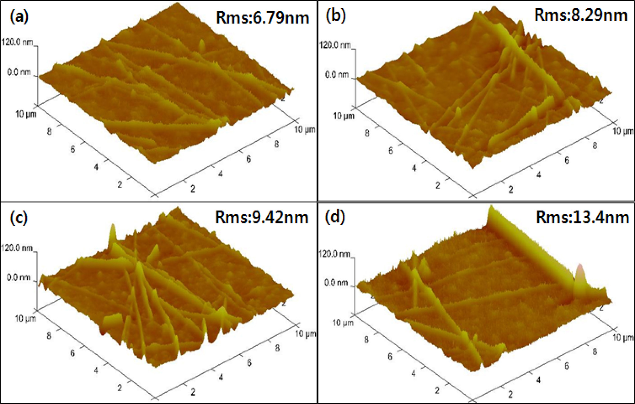
The PEDOT:PSS hole transfer layer was fabricated by
varying the speed of the spin coater from 1,000 rpm to 4,000 rpm. The surface
roughness of the hole transfer layer rose dramatically from 6.79 nm to 13.4 nm
as the speed increased from 1,000 rpm to 4,000 rpm, as shown in Figs. 7 and 8.
As the rotational speed of the spin coating increased, the thickness of the
hole transfer layer became thinner because the flexible substrate
was slightly bent at higher speeds. The surface roughness of
the layer was then deteriorated as the speed increased because thin film was
not uniformly formed due to the flexible PET film.
After coating PEDOT:PSS at 1,000 rpm on AgNW/PET
transparent electrode, the surface roughness was observed by spin-coating the
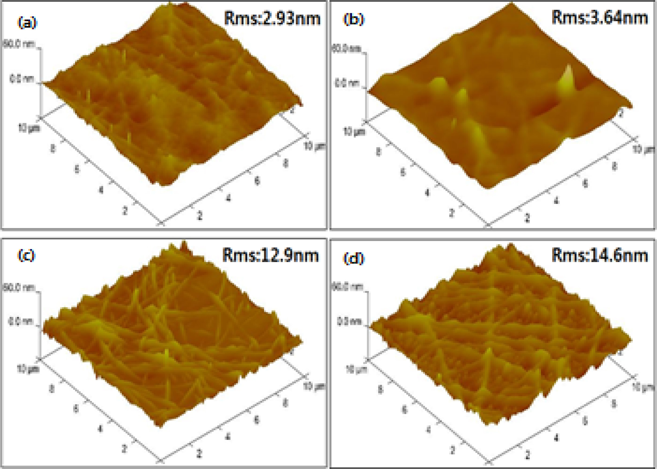
P3HT:PCBM active layer as a function of speed (1,000~4,000 rpm), as depicted in
Fig. 9. The surface roughness of the active layer (2.93 nm, 3.64 nm) coated at
speeds of 1,000 rpm and 2,000 rpm was much lower than that (6.79 nm) of
PEDOT:PSS layer coated at 1,000 rpm. However, it rose dramatically as the speed
increased. For OSCs using glass substrate, a vacuum was used to fix the rigid
substrate when using the spin coater. On the other hand, when the flexible PET
substrate was fixed using a vacuum, the film may be slightly bent due to the
vacuum force. Therefore, the thin film was formed thicker than the curvature of
the active layer thin film having the lowest surface roughness, resulting in an
improved surface roughness. As spinning speed increased (3000~4000 rpm), the
active layer became thinner. The thin film was not formed uniformly due to the
warping of the substrate, so the surface roughness was measured as high.
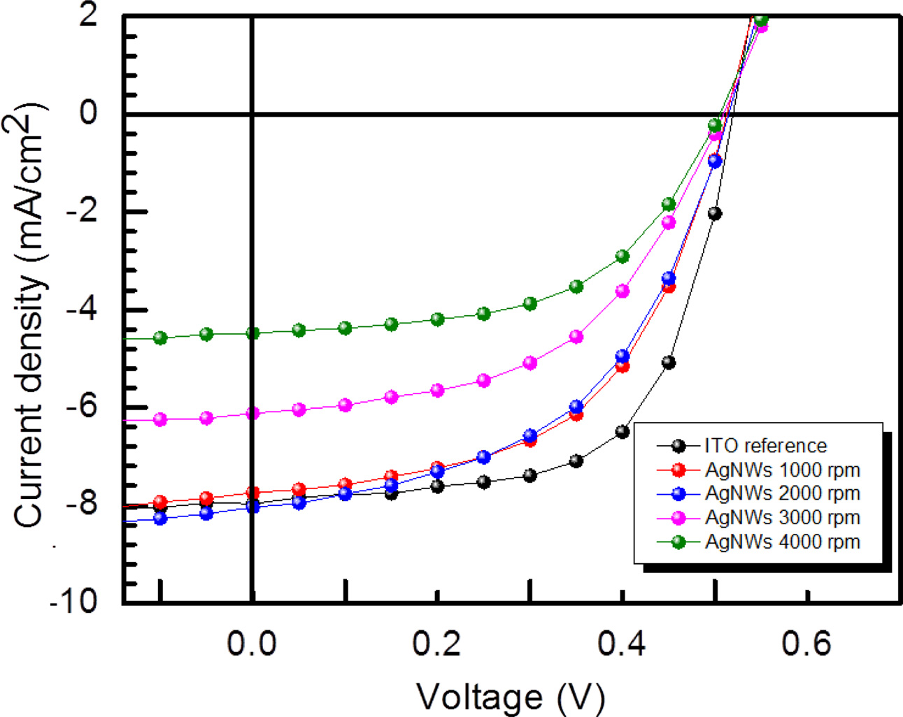
I-V characteristics of the flexible OSCs containing the
hole transfer layer and the active layer prepared at various speeds are shown
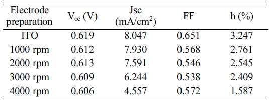
in Fig. 10. The efficiency of the OSCs fabricated by coating the active layer
at a speed of 1,000 to 4,000 rpm on the specimen coated with the hole transfer
layer at 1,000 rpm is listed in Table 2. The reference device with the ITO
electrode exhibited an open circuit voltage (Voc) of 0.619 V,
a short circuit current (Jsc) of 8.047 mA/cm2, a
fill factor (FF) of 0.651, and a power conversion efficiency (h)
of 3.247%, respectively [5, 15]. In comparison, the
devices with the AgNW electrode fabricated by coating the active
layer at 1,000 rpm showed Voc of 0.612 V, Jsc
of 7.930 mA/cm2, FF of 0.568, and h
of 2.761%, respectively. Although flexible OSCs were successfully fabricated,
the power conversion efficiency was relatively low because
there was no over-coating layer [5]. An over-coating layer and protection layer
for the AgNWs using conducting polymers and oxides was employed to lower the
surface roughness and improve the efficiency. But to simplify the process, no
over-coating layer was used. As the rotation speed rose, Voc,
Jsc, FF, and h decreased, likely due to the
deterioration of the surface roughness. As the speed increased, Jsc and
h became lower due to the difference in hardness between
glass and the PET substrate. Since the glass substrate is rigid, the substrate
was not warped due to the vacuum applied to the spin coater to hold the
substrate during coating, resulting in an improved surface roughness at 4,000
rpm. However, the PET substrate was slightly bent during the coating due to the
vacuum and the speed. OSCs using PET substrate were believed to have an
improved surface roughness due to the thick and smooth film of the hole
transfer layer and the active layer prepared at 1,000 rpm. Higher Jsc and
h were obtained at a low speed of 1,000 rpm due to the reduction in
resistance, and there was excellent hole injection due to the improved surface
roughness.
Flexible OSCs were fabricated using AgNWs as the
transparent electrode on the PET substrate. The power conversion efficiency of
OSCs using AgNWs was enhanced by using the over coating layer, resulting in an
improved surface roughness [5]. However, the over coating layer had a
disadvantage in that it cannot be applied to a large area and involved very
complicated processes. The effect of surface roughness on the
power conversion efficiency of the OSCs without the over
coating layer was studied in the present study. The OSCs was prepared using the
acryl resin coated PET substrate through the filtration/transfer method. The
sheet resistance of 30 Ω-1 and
the surface roughness of 10.5 nm were obtained, as listed in Table 1. The hole
transfer layer (PEDOT:PSS) and the P3HT:PCBM active layer were prepared at 1000
rpm, leading to an enhanced surface roughness. The best performance of the OSCs
prepared at low speed was observed. It could be concluded that the surface
roughness was mainly attributed to the output performance of the OSCs.
|
Fig. 3 (a) SEM image and (b) XRD diffraction of silver nanowires. |
|
Fig. 4 Transmittance of AgNW electrode on the glass and PET substrates prepared by spray and transfer coating methods. |
|
Fig. 5 AFM images of AgNW electrodes prepared by different substrate and coating method: (a) glass/spray, (b) glass/transfer, (c) PET/spray, and (d) PET/transfer. |
|
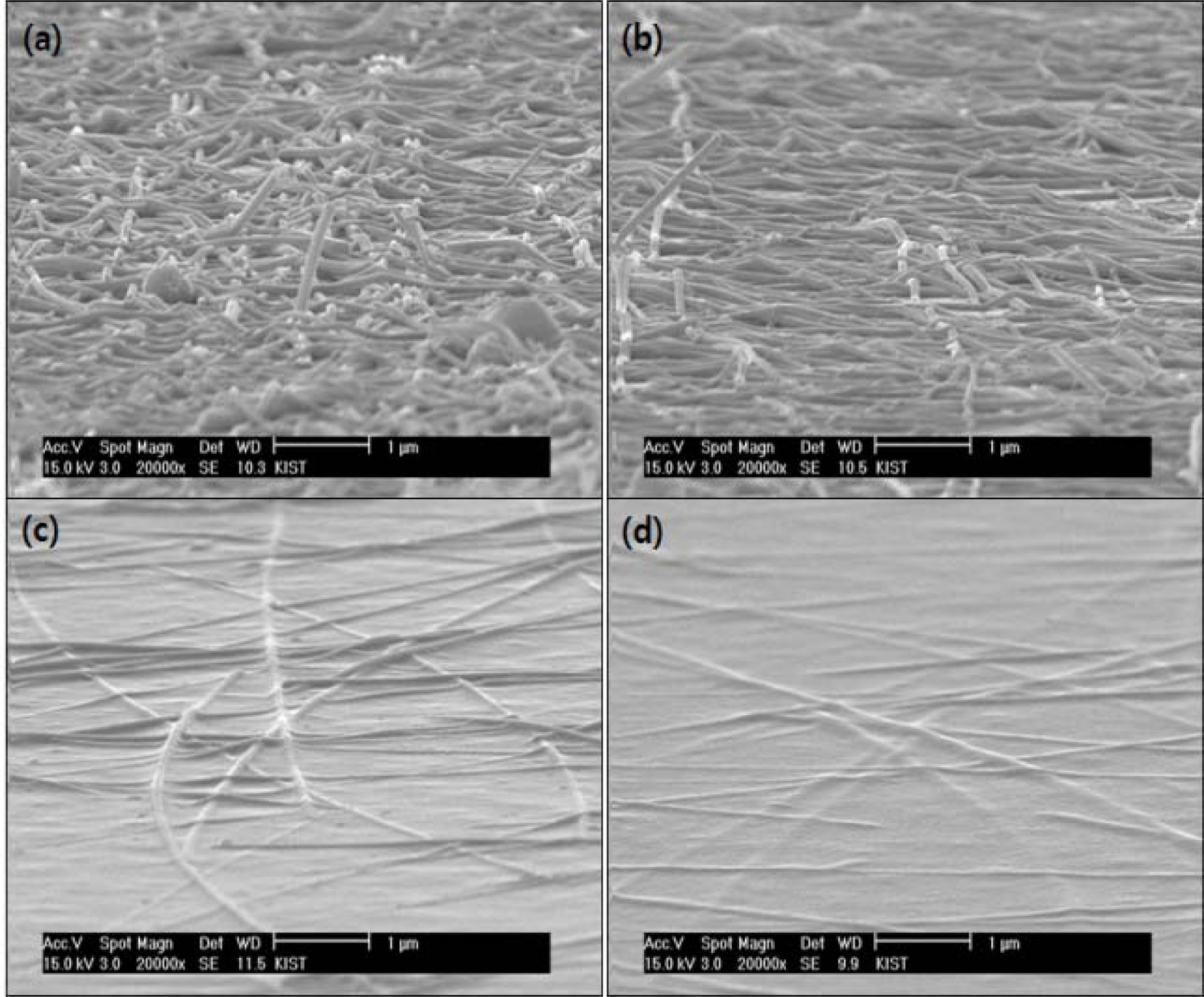
Fig. 6 SEM images of AgNW layers on (a,b) glass and (c,d) PET substrates prepared by (a,c) spray and (b,d) transfer method, respectively. |
|
Fig. 7 AFM images of the hole transfer layer as a function of the coating speed: (a) 1000 rpm, (b) 2000 rpm, (c) 3000 rpm, and (d) 4000 rpm, respectively. |
|
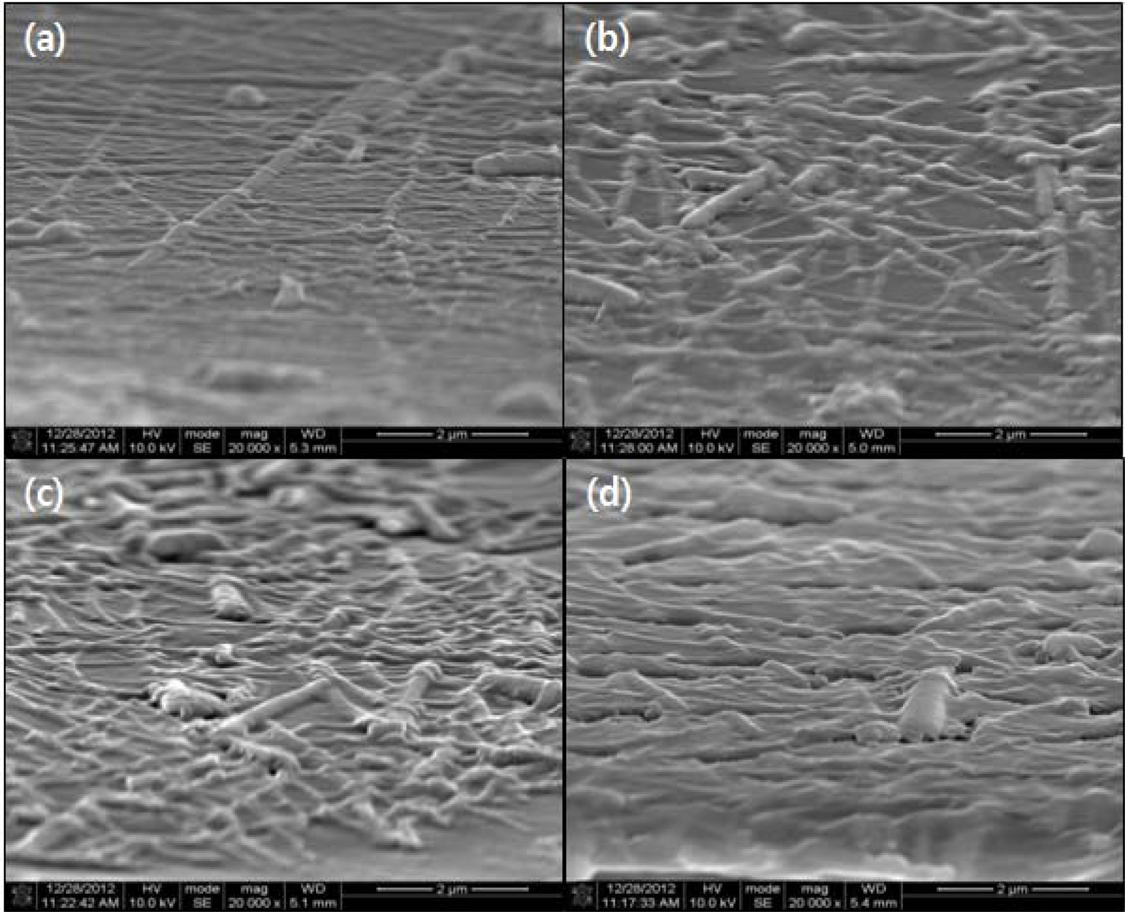
Fig. 8 SEM images of the hole transfer layers prepared by various speed: (a) 1000 rpm, (b) 2000 rpm, (c) 3000 rpm, and (d) 4000 rpm, respectively. |
|
Fig. 9 AFM images of the active layers coated on the hole transfer layer prepared at a speed of 1000 rpm. The active layers were prepared by varying the speed: (a) 1000 rpm, (b) 2000 rpm, (c) 3000 rpm, and (d) 4000 rpm, respectively. |
|
Fig. 10 I-V characteristics of the AgNWs/PEDOT:PSS/P3HT:PCBM/Lif:Al OSCs prepared by different coating speed. |
|
Table 1 Sheet resistance and surface roughness of OSCs on glass and PET with different coating methods |
|
Table 2 Performance of OSCs with the P3HT:PCBM active layer with various coating speeds |
A simple method for fabricating flexible OSCs, consisting
of an AgNW transparent electrode, a hole transfer
layer, an active layer, a LiF/Al electron collecting, and a top
electrode was proposed by using AgNWs to replace ITO OSCs. The AgNW transparent
electrode on acryl resin coated PET film was manufactured using the
filtration/transfer method. After spin-coating the PEDOT:PSS
layer and the P3HT:PCBM active layer at 1,000 rpm on
AgNW/PET transparent electrode, an improved surface roughness was achieved. The
OSCs with the AgNW electrode exhibited a relatively low Voc
of 0.612 V, Jsc of 7.930 mA/cm2, FF of
0.568, and h of 2.761%. However, Voc, Jsc,
FF, and h decreased as the coating speed was increased during the
formation of the hole transfer layer and the active layer due to undesired
leakage current caused by higher surface roughness. The surface roughness was
determined to be crucial for the output performance of OSCs. The AgNW
transparent electrode was highly suitable for an alternative transparent
electrode of ITO in OSCs.
- 1. C.-L. Kim, C.-W. Jung, Y.-J. Oh, and D.-E. Kim, NPG Asia Mater. 9 (2017) e438.
-

- 2. C.W. Tang, Appl. Phys. Lett. 48 (1986) 183-185.
-
- 3. J.Y. Kim, K. Lee, N.E. Coates, D. Moses, T. Nguyen, M. Dante, and A.J. Heeger, Science 317 (2007) 222-225.
-
- 4. C. Lee, R. Pandey, B. Wang, W. Choi, D. Choi, and Y.-J. Oh, Sol. Energy Mater. Sol. Cells 132 (2015) 80-85.
-
- 5. B.-Y. Wang, E. Lee, Y.-J. Oh, and H.W. Kang, RSC Adv. 7 (2017) 52914-52922.
-
- 6. B.J. Wiley, Y. Chen, J.M. McLellan, Y. Xiong, Z. Li, D. Ginger, and Y. Xia, Nano Lett. 7[4] (2007) 1032-1036.
-
- 7. C.J. Orendorff, L. Gearheart, N.R. Jana, and C.J. Murphy, Phys. Chem. Chem. Phys. 8 (2006) 165-170.
-
- 8. Y. Sun, B. Gates, B. Mayers, and Y. Xia, Nano Lett. 2 (2002) 165-168.
-
- 9. B.-Y. Wang, T. Yoo, J. Lim, B. Sang, D. Lim, W. Choi, D.K. Hwang, and Y.-J. Oh, Small 11 (2015) 1905-1911.
-
- 10. J. Xue, S. Uchida, B.P. Rand, and S.R. Forrest, Appl. Phys. Lett. 85 (2004) 5757-5759.
-
- 11. S.I. Na, S.S. Kim, J. Jo, and D.Y. Kim, Adv. Mater. 20 (2008) 4061-4067.
-
- 12. J. Xue, B.P. Rand, S. Uchida, and S.R. Forrest, Adv. Mater. 17 (2005) 66-71.
-
- 13. M. Vosgueritchian, D.J. Lipomi, and Z. Bao, Adv. Funct. Mater. 22 (2012) 421-428.
-
- 14. H. Hoppe and N.S. Saciciftci, J. Mater. Res. 19 (2004) 1924-1945.
-
- 15. Y. Kim, I. Lee, Y. Song, M. Lee, B. Kim, N. Cho, and D.Y. Lee, Electron. Mater. Lett. 10[2] (2014) 445-449.
-
- 16. D. Vikraman, A.A. Arbab, S. Hussain, N.K. Shrestha, S.H. Jeong, J. Jung, S.A. Patil, and H. Kim, ACS Sustainable Chem. Eng. 7 (2019) 13195-13205.
-
- 17. D.Y. Lee, H. Cho, D. Kang, J. Kang, M. Lee, B. Kim, and N. Cho, J. Korean Ceram. Soc. 51 (2014) 362-366.
-
- 18. S. Alwin, X.S. Shajan, K. Karuppasamy, and K.G.K. Warrier, Mater. Chem. Phys. 196 (2017) 37-44.
-
 This Article
-
2020; 21(1): 42-49
Published on Feb 28, 2020
- 10.36410/jcpr.2020.21.1.42
- Received on Jul 12, 2019
- Revised on Sep 27, 2019
- Accepted on Oct 7, 2019
Services
Shared
Correspondence to
- Young-Jei Oh
-
aOpto-electronic Materials & Devices Research Center, Korea Institute of Science and Technology, Seoul 02792, Korea
c- E-mail: youngjei@kist.re.kr
Clean-Energy Research Institute(CRI), Hanyang University, 222, Wangsimni-ro, Seongdong-gu, Seoul, 04763, Korea
E-mail: jcpr@hanyang.ac.kr