


- Morphological, structural, and optical properties of Co-doped ZnO NPs prepared by precipitation method
S. Iwana,*, D. Dianisyaa, Riser Fahdirana, Isnaenib, Esmar Budia, Anggara Budi Susilaa and Erfan Handokoa
aProgram Studi Fisika, FMIPA Universitas Negeri Jakarta, Jl. Rawamangun Muka No. 01, Rawamangun 13220, Indonesia
bResearch Center for Physics, Indonesian Institute of Sciences, Banten 15314, Indonesia
We have synthesized un-doped and Co-doped ZnO nanoparticles (NPs) by precipitation method at a temperature of 400 ℃ for 2 hours. According to the inorganic crystal structure database (ICSD) number #98-005-7478, the XRD pattern of ZnO NPs (average diameter of 99-144 nm) possess polycrystalline hexagonal wurtzite structure. The crystallite size of un-doped and 1.75 at.%, 3.79 at.%, 4.37 at.% Co-doped ZnO NPs are 20.81 nm, 19.84 nm, 43.85 nm, 37.95 nm, respectively. Meanwhile, the average micro-strain of the un-doped ZnO NPs and 1.75 at.%, 3.79 at.%, 4.37 at.% Co-doped ZnO NPs are 0.62%, 0.66%, 0.29%, 0.34%. These results confirm the crystallite size and micro-strain changing by Co incorporation. Further investigation, the Co incorporation into Zn site improve absorbance of ZnO NPs. Meanwhile, photoluminescence (PL) measurement shows that all ZnO NPs have one broad emission with centered peaks of 385 nm. It is indicating the substitution Zn2+ by Co2+ cause the distribution defect spread continuously in ZnO NPs structure
Keywords: un-doped and Co-doped ZnO NPs, polycrystalline, crystallite size, micro-strain, photoluminescence
As a metal oxide semiconductor, ZnO has broad potential applications such as photocatalyst [1], water disinfectant [2], sensor [3], solar cells [4], etc. It’s due to ZnO has a wide direct band gap energy of 3.37 eV and high exciton energy of 60 meV at room temperature [5-7].
ZnO has various different nanostructures and found in the wurtzite crystal structure [8-10]. A unique form of ZnO nanostructures such as NPs [1], nanocombs [11], nanotubes [5], nanorods [9], nanodisk [12], etc has a different application. Among these nanostructures, nano-crystallization of ZnO can control the optical and electrical properties due to quantum confinement [13, 14].
Technically, ZnO NPs can be synthesized by various methods such as hydrothermal [8], precipitation [15], laser ablation [13], sol-gel [16], etc. Compared to the other method, precipitation possesses cost-effective, scalable, and have been used to synthesized various different nanostructures [15]. The size of ZnO NPs was affected strongly by the synthesized method. According to the literature survey, the size of ZnO NPs can be obtained in the range of 10-30 nm by precipitation method [17, 18]. Meanwhile, by proper dopant, the recombination of electron-hole pairs of ZnO NPs can be controlled. Vanheusden et al [19] reported that Pb doping of ZnO powder cause band gap energy narrow and free-carrier concentration decrease by increasing Pb content. They also believed that the existence of Pb in ZnO structure acting as electron traps. Furthermore, when ZnO NPs doped by transition metal (TM) ions, energy level, and surface state will change [3].
Since the last decade, as TM element, Co-doped ZnO has been demonstrated as a dilute magnetic semiconductor (DMS) which potential in spintronic application [17]. Optically, Co-doped ZnO NPs are still become subject of interest. Pal et al reported that ZnO NPs with Co dopant indicate Co ions substitute into ZnO lattice [20] and by photoluminescence (PL) studies, the generation of the defects due to Co incorporation can be observed. Most recent, PL studies of Ni-Co doping ZnO NPs as a function of excitation wavelength shows shifting in near band edge (NBE) and red band (RB) emissions [1]. Further study, due to a blue shift in the absorbance spectrum, Co-doped ZnO NPs can be used as potential antibacterial rather than photocatalytic [21]. Nair et al believed that lower photodegradation is caused by faster recombination electron-hole pair [21, 22]. Nevertheless, in the last decade, Hong et al. believed that ZnO NPs has a potential application as a photocatalyst [23].
In this paper, we report the optical properties of un-doped and variation Co-doped ZnO NPs which synthesized by precipitation method at a calcination temperature of 400oC for 2 hours. The effect of Co dopant on morphology, structure, and optical properties of ZnO NPs will be discussed systematically.
Zinc chloride (ZnCl2) and Sodium Hydroxide (NaOH) were dissolved in de-ionized (DI) water (100 mL) to obtained 0.4 M and 0.8 M solution, respectively. The NaOH (0.4 M) solution was added into ZnCl2 (0.4 M) solution drop by drop under vigorous stirring without any heat treatment until a white suspension formed. To have Co-doped ZnO NPs, Zinc chloride (ZnCl2) and cobalt chloride (CoCl2) (5 wt.%, 10 wt.%, and 15 wt.%) as solution precursor dissolved into DI water (100 mL) stirred for 10 minutes until homogenous solution obtained. Then, to obtain precipitated of Zn(OH)2, each of the suspension solutions was centrifuged. Finally, to obtain powder ZnO NPs, the precipitation of Zn(OH)2 was calcined at the temperature of 400 oC for two hours.
Energy dispersive x-ray (EDS) was performed to confirm the atomic percentage of 5 wt.%, 10 wt.%, and 15 wt.% cobalt (Co) precursor which used as a dopant for ZnO NPs. The EDS results of ZnO NPs contain 5 wt.%, 10 wt.%, and 15 wt.% of Co precursor confirmed that the atomic percentage of Co are 1.75 at.%, 3.79 at.%, and 4.37 at.%, respectively. Hence, in the next part, we will consider the atomic percentage of Co as a dopant in ZnO NPs. Furthermore, the morphology, structure, absorbance, and photoluminescence of powder ZnO NPs have been observed by scanning electron microscopy (SEM) JEOL JSM-6510, X-ray diffraction (XRD) measurement with CuKa radiation (PAN-analytical), UV-Vis spectrophotometer UH 5300, and photoluminescence (PL) in the wavelength range of 300-900 nm, respectively.
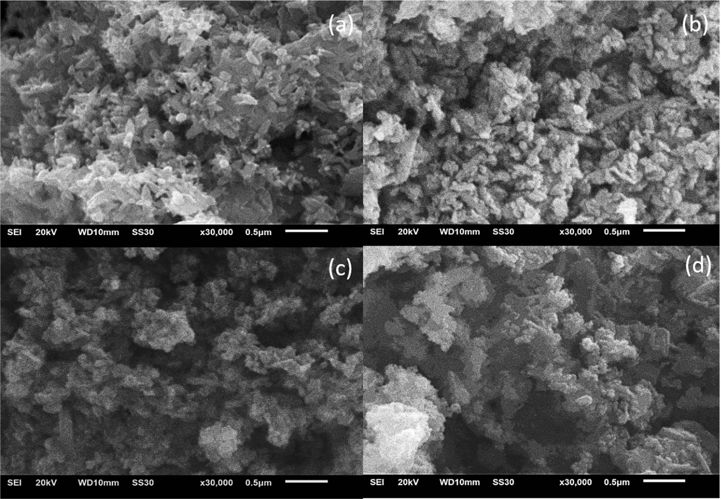
Fig. 1 shows SEM images of un-doped and Co-doped ZnO NPs. There is the aggregation of ZnO NPs due to high surface energy during calcination process [10, 23] and size dependence with Co incorporation. The ZnO NPs size increased by increasing Co incorporation. It can be confirmed that the average diameter of un-doped and 1.75 at.%, 3.79 at.%, 4.37 at.% Co-doped ZnO NPs is 88.16 nm, 99.62 nm, 140.66 nm, 143.8 nm, respectively. We predict the average diameter size of ZnO NPs increases linearly due to Co form oxide cluster which acts as heterogeneous nucleation sites during precipitation of the ZnO NPs.
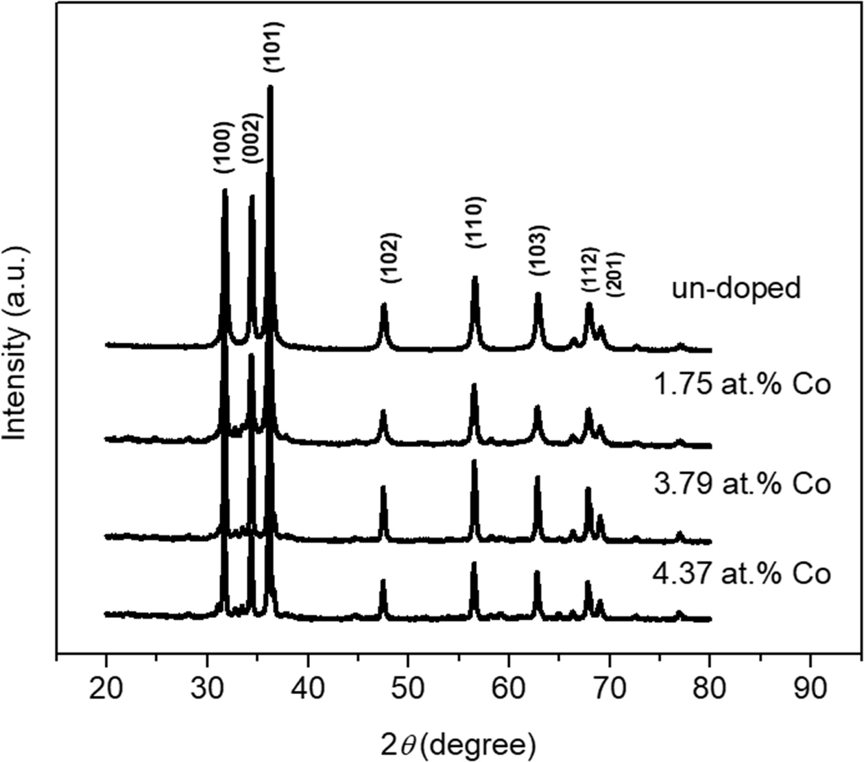
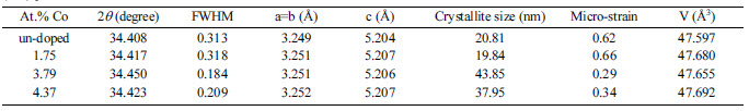
Fig. 2 shows XRD pattern of un-doped and 1.75 at.%, 3.79 at.%, 4.37 at.% Co-doped ZnO NPs. According to the inorganic crystal structure database (ICSD) number #98-005-7478, the XRD pattern of ZnO NPs possess polycrystalline hexagonal wurtzite structure. There is no other phase from Co as the dopant and no modification of crystal structure. We predict, the Co2+ could substitute Zn2+ due to the similarity of the ionic radius. According to our previous results [10], we focus on (002) plane as a preferred orientation to investigate the effect of Co doping. We predict that Co2+ substitute Zn2+ randomly and cause lattice distortion in the crystal structure. As results, the full width at half maximum (FWHM) of ZnO NPs changes non-linearly. As well known, according to Debye-Scherer’s equation [24, 25], the FWHM can be used to determine the crystallite size of the structure. The crystallite size of un-doped and 1.75 at.%, 3.79 at.%, 4.37 at.% Co-doped ZnO NPs is 20.81 nm, 19.84 nm, 43.85 nm, 37.95 nm, respectively (Table 1). Furthermore, the average micro-strain of the un-doped ZnO NPs and various Co-doped ZnO NPs can be determined by the Stokes-Wilson equation [9]. The micro-strain of un-doped and 1.75 at.%, 3.79 at.%, 4.37 at.% Co-doped ZnO NPs are 0.62%, 0.66%, 0.29%, 0.34%. According to these results, the crystallite size and micro-strain changing by Co incorporation. It can be observed that the crystallite size and micro-strain for 1.7 at.% Co-doped ZnO NPs is smaller and larger than un-doped. We predict the 1.7 at.% Co-doped ZnO NPs is the proper composition to decrease nucleation and growth rate of ZnO NPs during the growth process. Meanwhile, the other compositions have higher crystallite size compared to un-doped and 1.7 at.% Co-doped ZnO. As reported by other, we also believed that the increasing crystallite size by increasing Co2+ ions due to the less solubility of Co in ZnO matrix [21].
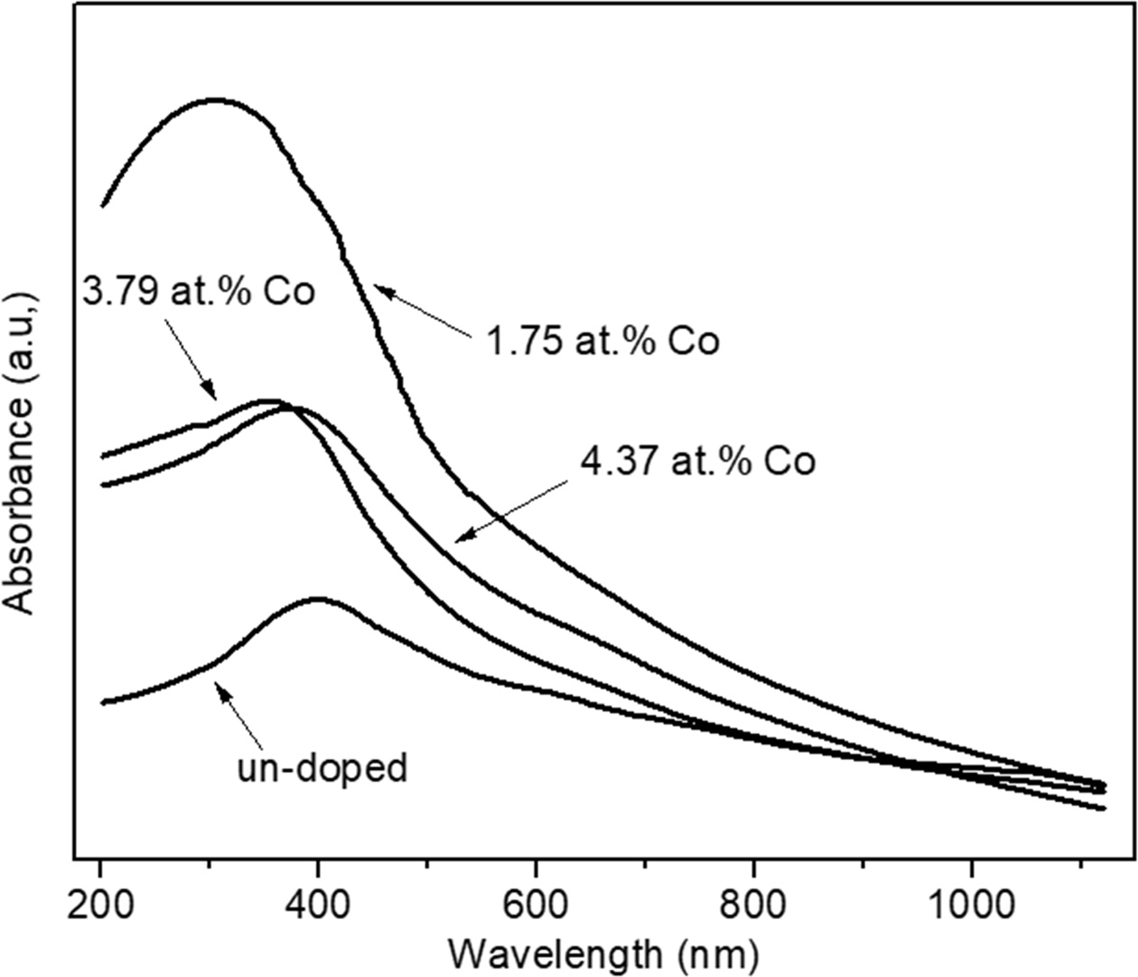
Fig. 3 shows the absorption spectra of un-doped and variation Co-doped ZnO NPs. All the spectra pattern has broad absorption in the range UV-Vis wavelength in the range of 300-600 nm. It can be seen that the un-doped ZnO NPs has the lowest absorption and incorporation Co of 1.75 at.% has the strongest broad absorption at the peak of 325 nm. Furthermore, instead of cause lattice distortion in the crystal structure, the incorporation of Co into ZnO site may cause the interaction between s and p orbitals of ZnO with localized electrons in d orbital which associated with the doped Co2+ ions. Therefore, it causes a change in the band structure of ZnO [20]. As results, the absorbance of Co-doped ZnO will be stronger than un-doped ZnO. Meanwhile, the peak of the absorption spectra of Co-doped ZnO shifted to the lower wavelength (blueshift). The blueshift indicating that the Co incorporation in ZnO structure increase band gap energy. As well known, it is due to the Burstein-Moss effect which explains the carrier concentration cause the Fermi energy overlap with the conduction band [25].
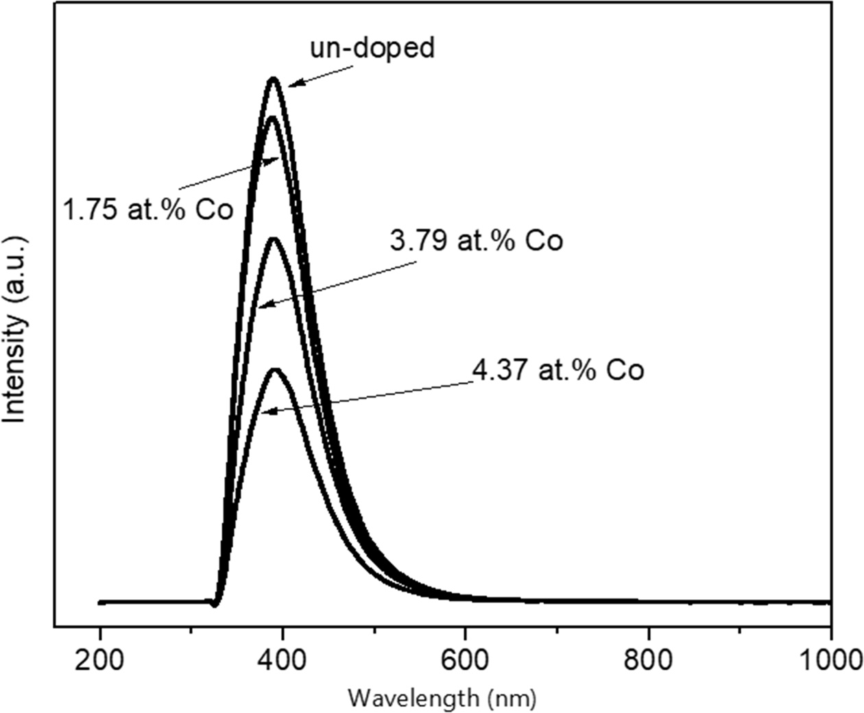
In order to detect the presence of the defects in ZnO NPs, we performed PL measurement at room temperature. Fig. 4 show a room temperature PL spectrum of un-doped and variation Co-doped ZnO NPs. Typically, PL spectra of ZnO NPs has two emissions, i.e. excitonic-related UV emission and defect-related green band (GB) emission [5]. Huang et al. reported that the Co incorporation in the ZnO structure has typical emissions of ZnO with broad UV and visible emissions [26]. However, our PL measurement shows one broad spectrum for all samples with the centered peaks of 385 nm. It can be seen from the Fig. 4, the PL spectra intensity decreases gradually even though the absorption is higher by presence of Co. It is indicating the substitution Zn2+ by Co2+ cause the distribution defect spread continuously in ZnO NPs structure. In our case, beside the defects such as oxygen vacancy (Vo), interstitial Zn (Zni), zinc vacancy (Vzn), interstitial oxygen (Oi) lie continuously in the structure, by increasing Co content (1.75 at.%, 3.79 at.% and 4.37 at.%) will generate complex defect energy levels between valence and conduction band. Therefore, the Fermi level will move close to the conduction band due to the carrier concentration increase. This phenomenon is called by the Burstein-Moss effect [26]. As a result, a non-radiative transition of Co-doped ZnO NPs is more dominant compared to un-doped ZnO NPs.
|
Fig. 1 SEM images of ZnO NPs: (a) un-doped, (b) 1.75 at.% Co, (c) 3.79 at.% Co, (d) 4.37 at.% Co. |
|
Fig. 2 XRD pattern of un-doped and Co-doped ZnO NPs. |
|
Fig. 3 The absorption spectra of un-doped and variation Co-doped ZnO NPs. |
|
Fig. 4 Room temperature PL spectra of un-doped and variation Co-doped ZnO NPs. |
|
Table 1 The variation data of full width at half maximum (FWHM), crystallite size, and strain of un-doped and Co-doped ZnO NPs at (002) plane. |
In conclusion, ZnO NPs (NPs) synthesized by precipitation method at a temperature of 400 oC for 2 hours. The ZnO NPs have doped by cobalt (Co) with atomic percentage 0 at.% (un-doped), 1.75 at.%, 3.79 at.%, and 4.37 at.% have average particle size are 88.16 nm, 99.62 nm, 140.66 nm, 143.8 nm, respectively. The XRD pattern of ZnO NPs possess polycrystalline hexagonal wurtzite structure with no other phase. Optically, ZnO with Co dopant has stronger absorption. Meanwhile, the peak PL intensity decrease by Co incorporation.
Financial support from hibah penelitian kompetitif Universitas Negeri Jakarta no. 12/KOMP-UNJ/LPPM-UNJ/II/2018 is gratefully acknowledged.
- 1. P. Pascariu, I.V. Tudose, M. Suchea, E. Koudoumas, N. Fifere, and Appl. Surf. Sci. 448[1] (2018) 481-488.
-

- 2. E.A.S. Dimapilis, C. Hsu, and R.M.O. Mendoza, Sustain. Environ. Res. 28[2] (2018) 47-56.
-
- 3. U. Godavarti, V.D. Mote, M.V.R. Reddy, P. Nagaraju, Y.V. Kumar, K.T. Dasari, and M.P. Dasari, Phys. B Phys. Condens. Matter. 553 (2018) 151-160.
-
- 4. D. Liu and T.L. Kelly, Nat. Photonics. 8 (2014) 133-138.
-
- 5. S. Iwan, J.L. Zhao, S.T. Tan, and X.W. Sun, Vacuum. 155 (2018) 408-411.
-
- 6. S. Iwan, S. Bambang, J.L. Zhao, S.T. Tan, H.M. Fan, L. Sun, S. Zhang, H.H. Ryu, and X.W. Sun, Phys. B Condens. Matter. 407 (2012).
-
- 7. S. Iwan, J.L. Zhao, S.T. Tan, S. Bambang, M. Hikam, H.M. Fan, and X.W. Sun, Mater. Sci. Semicond. Process. 30 (2015) 263-266.
-
- 8. M. Søndergaard, E.D. Bøjesen, M. Christensen, and B.B. Iversen, Cryst. Growth Des. 11[9] (2011) 4027-4033.
-
- 9. N.A. Putri, V. Fauzia, S. Iwan, L. Roza, A.A. Umar, and S. Budi, Appl. Surf. Sci. 439 (2018) 285-297.
-
- 10. I. Sugihartono, D. Dianisya, and I. Isnaeni, Crystal structure analyses of ZnO nanoparticles growth by simple wet chemical method, in: IOP Confrence Ser. Mater. Sci. Eng., 2018: p. 012077.
-
- 11. J.X. Wang, X.W. Sun, A. Wei, Y. Lei, X.P. Cai, J.X. Wang, X.W. Sun, and A. Wei, 233106 (2006) 10-13. doi:10.1063/1.2210078.
-
- 12. X. Qu and D. Jia, Mater. Lett. 63 (2009) 412-414.
-
- 13. H. Usui, Y. Shimizu, T. Sasaki, and N. Koshizaki, J. Phys. Chem. B 109[1] (2005) 120-124.
-
- 14. Y. Wang and N. Herron, J. Phys. Chem. 95 (1991) 525-532.
-
- 15. D. Raoufi, Renew. Energy. 50 (2013) 932-937.
-
- 16. A.K. Zak, M.E. Abrishami, W.H.A. Majid, R. Yousefi, and S.M. Hosseini, Ceram. Int. 37 (2011) 393-398.
-
- 17. N. Hasuike, R. Deguchi, H. Katoh, K. Kisoda, K. Nishio, T. Isshiki, and H. Harima, J. Phys. Condens. Matter. 19[36] (2007).
-
- 18. A. Samanta, M.N. Goswami, and P.K. Mahapatra, Phys. E Low-Dimensional Syst. Nanostructures 104 (2018) 254-260.
-
- 19. K. Vanheusden, W.L. Warren, J.A. Voigt, C.H. Seager, D.R. Tallant, K. Vanheusden, W.L. Warren, J.A. Voigt, C.H. Seager, and D.R. Tallant, Appl. Phys. Lett. 67 (1995) 7-10.
-
- 20. B. Pal and P.K. Giri, J. Appl. Phys. 108 (2014) 084322.
-
- 21. M.G. Nair, M. Nirmala, K. Rekha, and A. Anukaliani, Mater. Lett. 65 (2011) 1797-1800.
-
- 22. R. Ullah and J. Dutta, J. Hazard. Mater. 156 (2008) 194-200.
-
- 23. R.Y. Hong, J.H. Li, L.L. Chen, D.Q. Liu, H.Z. Li, Y. Zheng, and J. Ding, Powder Technol. 189 (2009) 426-432.
-
- 24. I. Sugihartono, E. Handoko, V. Fauzia, A. Arkundato, and L.P. Sari, Makara J. Technol. 22 (2018) 13-16.
-
- 25. S.A. Ansari, A. Nisar, B. Fatma, W. Khan, and A.H. Naqvi, Mater. Sci. Eng. B Solid-State Mater. Adv. Technol. 177 (2012) 428-435.
-
- 26. L. Huang, Y. Hao, and M. Hu, Mater. Sci. Semicond. Process. 74 (2018) 303-308.
-
 This Article
-
2019; 20(5): 518-521
Published on Oct 31, 2019
- 10.36410/jcpr.2019.20.5.518
- Received on Apr 30, 2019
- Revised on Jun 26, 2019
- Accepted on Aug 2, 2019
Services
- Abstract
introduction
experimental methods
results and discussion
conclusions
acknowledgement
- References
- Full Text PDF
Shared
Correspondence to
- S. Iwan
-
Program Studi Fisika, FMIPA Universitas Negeri Jakarta, Jl. Rawamangun Muka No. 01, Rawamangun 13220, Indonesia
Tel : +62 21 4894909
Fax: +62 21 4894909 - E-mail: isugihar@hotmail.com and iwan-sugihartono@unj.ac.i
Clean-Energy Research Institute(CRI), Hanyang University, 222, Wangsimni-ro, Seongdong-gu, Seoul, 04763, Korea
E-mail: jcpr@hanyang.ac.kr