


- Microstructure and depolarization behavior of ZnO-added (Bi0.5Na0.5)0.94Ba0.06TiO3 lead-free ceramics sintered at different heating rates
Han-li Lian* and Rui-xue Cheng
School of Science, Xi’an University of Posts and Telecommunications, Xi’an 710121, P.R. China
The ZnO-added (Bi0.5Na0.5)0.94Ba0.06TiO3 (denoted as BNBTZ) ceramics were prepared by means of a solid-state reaction method. The ceramics were sintered at 0.5 ℃/min and 9 ℃/min. Their microstructure, phase structure, piezoelectric, and dielectric properties were investigated. Both the ceramics exhibit dense microstructures. Compared to the ceramics sintered at 0.5 ℃/min, those sintered at 9 ℃/min have smaller grains. The X-ray diffraction (XRD) and energy-dispersive spectrum reveal that the ceramics exhibit two phases, i.e., BNBTZ phase with perovskite structure and ZnO phase. The movement of the peak position implies enlargement of the crystallite lattice due to the entrance of Zn2+ ions into the lattice. The effect of sintering rates on depolarization behavior was discussed.
Keywords: Lead-free ceramics, Microstructure, Piezoelectric properties, Depolarization, Sodium bismuth titanate
Sodium bismuth titanate (Na0.5Bi0.5TiO3, BNT) is one of the lead-free piezoelectric material. Various dopants have been added into BNT for improving their electrical properties. For examples, BNT-(K0.5Bi0.5)TiO3-BiCoO3 [1], BNT-BaTiO3 [2-3], BNT-KNbO3 [4], BNT-BiAlO3 [5-6], BNT-SrTiO3 [7], BNT-K0.5Na0.5NbO3-BaTiO3 [8], Bi0.5K0.5TiO3-BNT-SrTiO3 [9], Na0.47Bi0.47Ba0.06TiO3-BiFeO3 [10], (1-x)(K1-yNay)NbO3-x(Bi1/2Na1/2)ZrO3 [11], K0.95Na0.05Ta1-xNbxO3 [12], and so on, have been widely studied. Depolarization behavior of piezoelectric materials is very important for high-temperature application. As the temperature is increased up to depolarization temperature, piezoelectric properties tend to disappear. Tuan et al. studied the relaxation behavior of ZnO-doped 0.48BaZr0.2Ti0.8O3-0.52Ba0.7Ca0.3TiO3 ceramics [13]. Zhang et al. reported that the addition of ZnO nanoparticles into (Bi0.5Na0.5)0.94Ba0.06TiO3 could significantly increase the depolarization temperature [14]. They believe that ZnO nanoparticles on the grain boundaries of (Bi0.5Na0.5)0.94Ba0.06TiO3 are the source to maintain thermal stability of the depolarization. Under the applied electric field, the ZnO grains can be polarized to form a local electric field, which compensates for the depolarization as the applied electric field is removed (called an interface effect) [14-15]. However, Mahajan et al. proposed that the thermal depolarization was not related to interface effect, and it was due to the change of phase transition between the tetragonal phase and the rhombohedral phase [16].
For preparing ceramics, calcination and sintering paramters are very important [17, 18]. For example, heating rate can influence electrical properties of the ceramics obviously [18]. In this work, the ceramics (Bi0.5Na0.5)0.94Ba0.06TiO3 with the addition of 30% mol ZnO were prepared by means of the solid-state reaction method. It is found that Zn2+ ions can both dissolve into the (Bi0.5Na0.5)0.94Ba0.06TiO3 lattice and also exist as a ZnO secondary phase on the grain boundaries. In order to detect interface effect and doping effect, the heating rates for sintering ceramics were chosen as 0.5 oC/min and 9 oC/min. The depolarization behavior of the ceramics sintered at different heating rates was studied via dielectric spectra and ex-situ d33 measurement.
The (Bi0.5Na0.5)0.94Ba0.06TiO3-30% mol ZnO (denoted as BNBTZ) ceramics were sintered via the solid-state reaction method. The raw materials are Na2CO3 (99.8%), TiO2 (³98.0%), Bi2O3 (≥98.9%), and BaCO3 (≥99.0%) powders. These powders were dried at 120 °C for 24 hours and then weighed according to the chemical formula of (Bi0.5Na0.5)0.94Ba0.06TiO3. The powders were ball milled for 24 hours and then dried. The dried powders were calcined at 920 oC. The dwelling time during calcination is 3 hours. The commercial ZnO nanoparticles (≥99%, 25 nm) were added into the calcined powders according to the composition of BNBTZ and ball milled in ethanol for 8 hours. After drying, the powders were pressed into pellets by using cold isostatic pressing under 200 MPa. The BNBTZ ceramics were sintered at 1040 oC for 2 hours in the conventional furnace with the heating element of silicon molybdenum. The heating rates are 0.5 oC/min and 9 oC/min, respectively. During the sintering process between 500 oC and 1040 oC, the required time is 18 hours and 1 hour for the heating rates of 0.5 oC/min and 9 oC/min, respectively.
The X-ray diffraction (XRD) of Rigaku D/MAX 2550 was used to detect phase structure. Scanning electron microscope (SEM) images of the ceramics were observed via Nova Nano 450 SEM equipped with energy-dispersive spectrum (EDS) attachment. The average grain size of the ceramics was calculated via NANO measure software. The ceramics were polarized in silicone oil at room temperature under 5 kV × mm-1 for 30 min. The piezoelectric constant d33 was measured by using a ZJ-4A d33 meter. Dielectric properties were measured on a dielectric spectrometer (Novocontrol Concept 80).
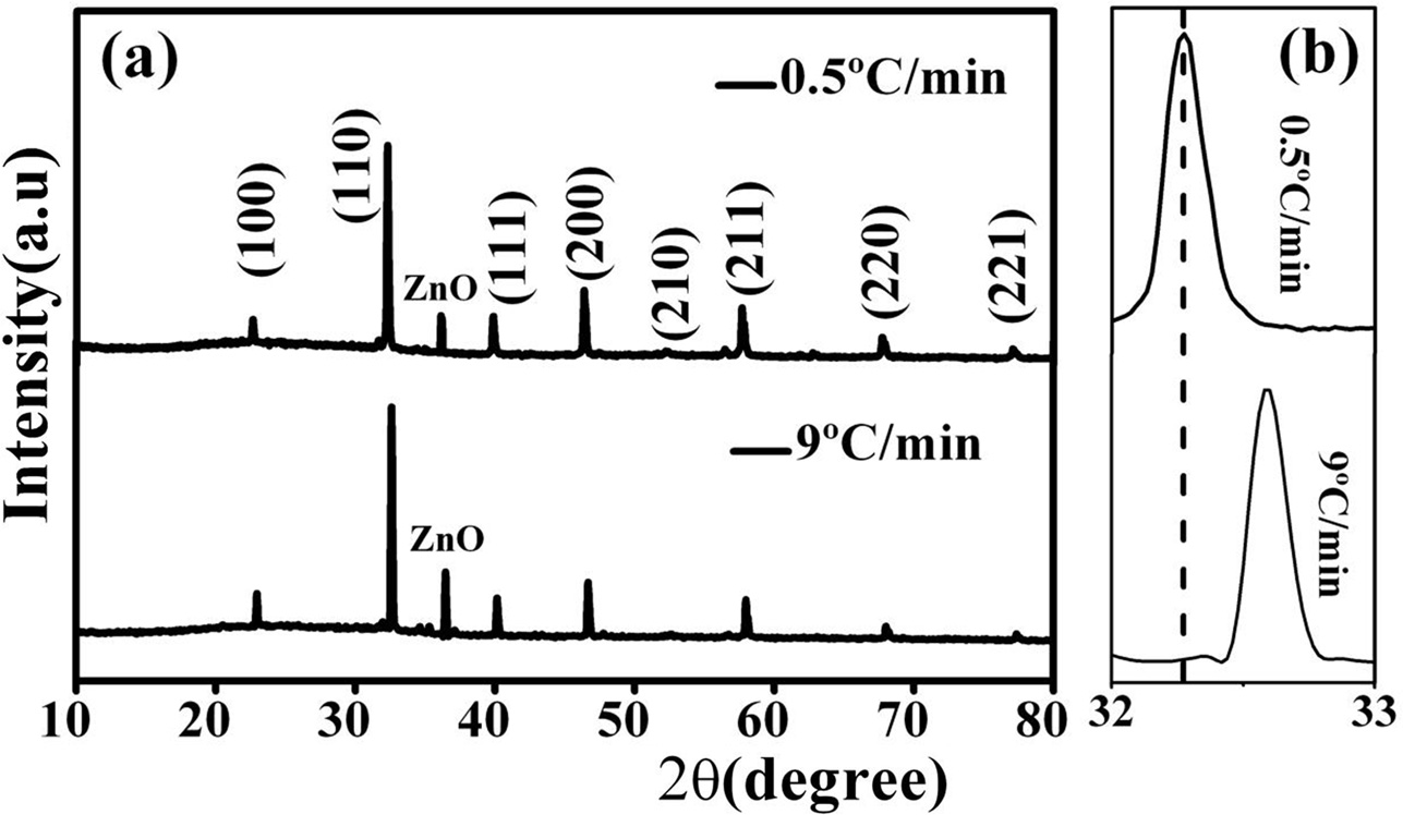
Fig. 1(a) exhibits the XRD curves of the ceramics sintered at the different heating rates. Both the ceramics exhibit two phases, i.e., BNBTZ phase and ZnO phase. The ZnO phase is in accordance with JCPDS No. 79-2205, implying that ZnO exists as a secondary phase in the samples. The enlarged pattern of the peaks corresponding to the maximum intensity around 32° is shown in Fig. 1(b). Compared to the XRD peak of the ceramic sintered at 9 °C/min, that of the ceramic sintered at 0.5 °C/min moves to lower 2 theta direction. According to the Bragg equation, the crystallite lattice of the ceramic sintered at 0.5 °C/min expands compared to that of the ceramic sintered at 9 °C/min. Smaller heating rate means the longer time the samples are exposed in a high-temperature environment. For example, during the sintering process in which the temperature is raised from 500 °C to 1040 °C, the required time is 18 hours and 1 hour for the heating rates of 0.5 °C/min and 9 °C/min, respectively. It is reasonable to expect that the samples have sufficient time and more Zn2+ ions can enter into the crystallite lattice as the rate is low. The radii of Ti4+ and Zn2+ are 0.605 Å and 0.740 Å for CN=6, respectively. The Ti4+ and Zn2+ ions have similar radii. The Zn2+ ions should occupy the Ti4+ site due to their similar radii. The substitution of Zn2+ for Ti4+ can cause lattice expansion because of the larger radius of Zn2+ compared to that of Ti4+. More Zn2+ ions have entered into the crystallite lattice of the ceramic sintered at 0.5 °C/min. So, the ceramics sintered at 0.5 °C/min exhibit enlarged lattice and the XRD peaks move towards lower 2 theta direction. More Zn2+ ions can enter into the lattice of the sample sintered at 0.5 °C/min compared to that sintered at 9 °C/min, which can be further verified via the EDS results, as shown later.
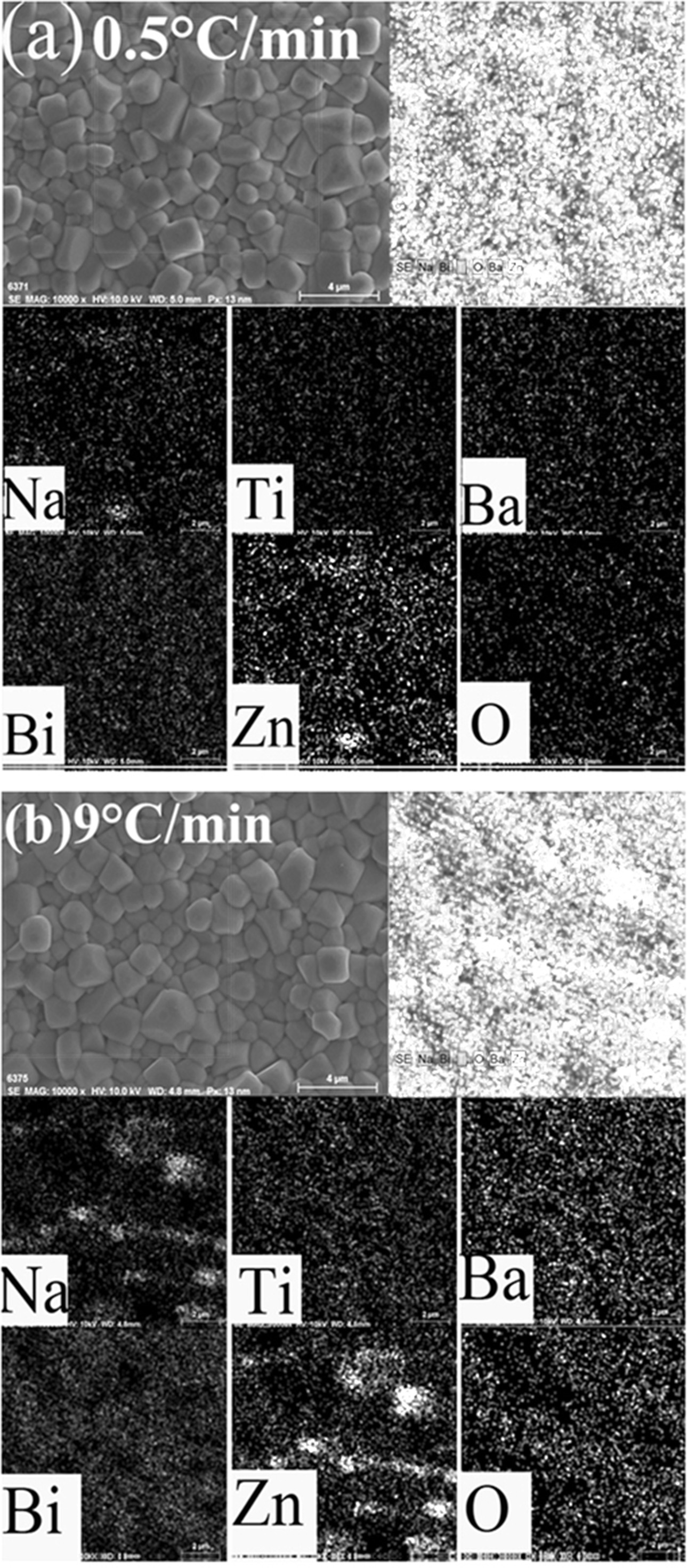
The SEM images of the ceramics and the corresponding EDS results are shown in Fig. 2. The ceramics exhibit dense microstructures, corresponding to high relative densities (>95%). The mean grain sizes of the ceramics sintered at 0.5 °C/min and 9 °C/min are 1.5 ± 0.2 μm and 0.9 ± 0.2 μm, respectively. The ceramics sintered at relatively low heating hates have relatively large grains, which can be attributed to longer time the samples exposing in the high-temperature environment. The EDS results demonstrate that the Zn element was found in both samples. Compared to the ceramic sintered at 9 °C/min, the sample sintered at 0.5 °C/min exhibits a uniform distribution of Zn element. In the ceramic sintered at 9 °C/min, there is an accumulation of Zn element. As mentioned above, the XRD results show that more Zn2+ ions can enter into the crystallite lattice in the ceramics sintered at 0.5 °C/min. Here, the EDS results are consistent with the XRD results.
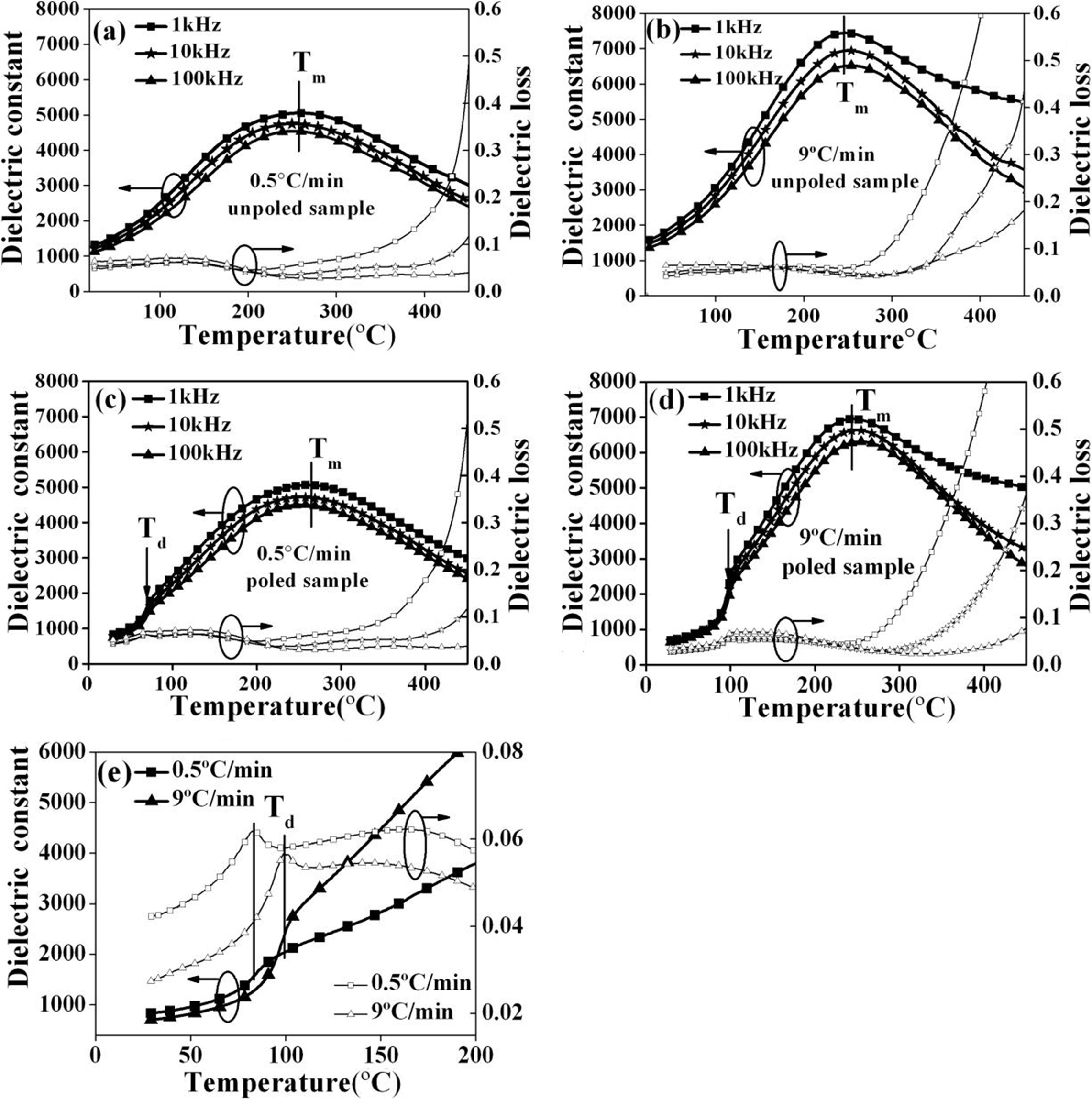
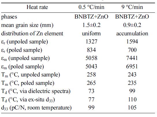
The microstructure and electrical properties of the ceramics sintered at the different heating rates are compared in Table 1. The dielectric constant of the unpoled ceramics sintered at 0.5 °C/min and 9 °C/min measured at 1 kHz and room temperature are 1327 and 1594, respectively. The values are comparable with those reported by others [2, 3, 19]. For example, Jing et al. reported that the (Bi0.5Na0.5)0.94Ba0.06TiO3 ceramics exhibit the er value 1597 [19]. Figs. 3(a,b) show the dielectric spectra with increasing temperature for the unpoled ceramics. For both samples, the dielectric constant decreases as the frequency increases at a given temperature. For a given frequency, the dielectric constant increases to a maximum and then decreases. The temperature corresponding to the maximum was denoted as Tm, at which the transition between the ferroelectric phase and the paraelectric phase occurs [19, 20]. The dielectric spectra of the poled ceramics are shown in Fig. 3(c,d). Compared to the unpoled ceramics, the poled ceramics exhibit a new dielectric anomaly around the temperature denoted as Td. Below Td, the dielectric constant at different frequencies tends to merge together. The dielectric constant rises abruptly at Td. Correspondingly, there appears a sharp peak on the dielectric loss ~ temperature curves. The phenomenon was always observed in the BNT -based ceramics [2, 21]. An enlarged view of the dielectric spectrum around Td is compared in Fig. 3(e). The temperature Td is always being used to determine depolarization temperature in BNT -based materials [21]. For the ceramics sintered at 0.5 oC/min and 9 oC/min, the Td values are 73 oC and 99 oC, respectively. The ceramic sintered at the relatively low heating rate has a lower depolarization temperature.
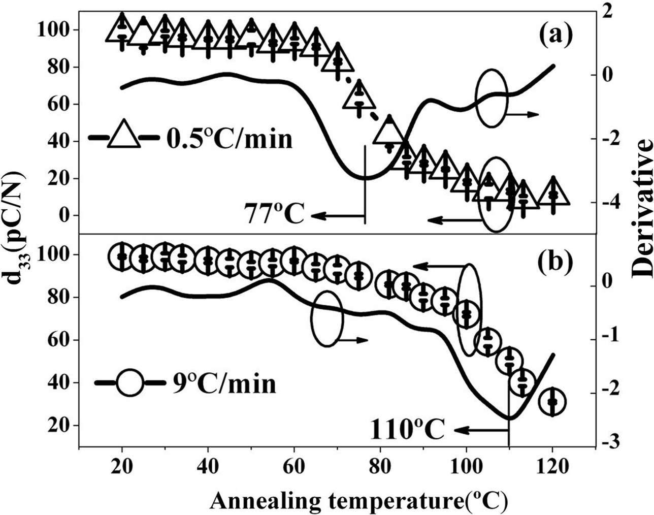
The poled ceramics sintered at 0.5 oC/min and 9 oC/min have d33 of 99 pC/N and 105 pC/N at room temperature, respectively. Via the variation of d33 as a function of annealing temperature, depolarization temperature of the ceramics can also be obtained from the ex-situ d33 measurement [22]. Davies et al. pointed out that depolarization temperature can be determined as the annealing temperature at which the d33 is decreased to half of its original value [19]. Anton et al. reported that the depolarization temperature can be expressed by the temperature corresponding to the steepest decrease of d33 [23]. Here, in order to provide evidence for depolarization temperature, the polarized samples were annealed at various temperatures from room temperature to 120 °C. The dwelling time during annealing was chosen as 30 min. After annealing at a given temperature, the d33 was measured. The changes of d33 as a function of annealing temperatures are shown in Fig. 4. The depolarization temperature of the ceramics was determined as the peak temperature on the corresponding first-order derivative curves. The depolarization temperatures of the ceramics sintered at 0.5 °C/min and 9 °C/min were determined to be 77 °C and 110 °C via the ex-situ d33 measurement, respectively. The samples sintered at lower heating rates exhibit lower depolarization temperature.
For a given sample, the value of depolarization temperature is different for the different measurement methods, as reported by others [1, 19]. Both the results of the change in d33 with annealing temperature and dielectric spectra confirm that the depolarization temperatures of the ceramics sintered at 9 °C/min are higher than those of the samples sintered at 0.5 °C/min. The above results demonstrate that a higher sintering rate corresponds to higher depolarization temperature. As the sintering rate is low, more Zn2+ ions enter into the crystal lattice, and ZnO amount on the grain boundary becomes less. For the high heating rate, more ZnO phase exists on the boundaries. Zhang et al. suggested that localized field formed by the polarization of the ZnO phase on the grain boundary compensates the depolarization field and causes an increase of depolarization temperature [11]. On the other hand, some Zn2+ ions have entered into the BNBT lattice. The doping of cations can always cause a change in depolarization temperature. Mahajan et al. reported that the shift in depolarization temperature is related to the doping of Zn2+ into the 0.94Bi0.5Na0.5TiO3-0.06BaTiO3 lattice [15]. In other ceramics, such as Pb(Mg1/3Nb2/3)0.9Ti0.1O3, the substitution of Zn2+ can increase the depolarization temperature [24]. These results suggest that the change of depolarization temperature of the BNBTZ ceramics should be associated with the entrance of Zn2+ ions into the BNBT lattice. Generally, more cations entering into the lattice induce higher depolarization temperatures. The lower the heating rate, the more ions enter into the BNBT lattice, but the depolarization temperature decreases. Therefore, we believe that the interface effect is majorly affecting depolarization temperature.
|
Fig. 1 XRD curves of the ceramics sintered at 0.5 oC/min and 9 oC/min (a), and the enlarged pattern around 32o (b). |
|
Fig. 2 SEM images and the corresponding EDS results for the ceramics sintered at 0.5 oC/min (a) and 9 oC/min (b). |
|
Fig. 3 Temperature-dependent dielectric constant and dielectric loss of the unpoled (a,b) and poled ceramics (c,d); the enlarged pattern of dielectric spectra around Td (e). |
|
Fig. 4 Fig. 4. Effect of the annealing temperatures on d33 values of the poled ceramics. The corresponding first-order derivative curves are also shown. |
|
Table 1 Comparision of microstructure and electrical properties of the ceramics sintered at 0.5 oC/min and 9 oC/min. The values of er were obtained at 1 kHz and room temperature. |
In summary, microstructure and depolarization behavior of the (Bi0.5Na0.5)0.94Ba0.06TiO3-30% mol ZnO ceramics sintered at different heating rates were investigated. The XRD results demonstrate that some Zn2+ ions exist in the ceramics as the secondary phase of ZnO, and some Zn2+ ions have entered into the crystallite lattice. For the ceramic sintered at 0.5 °C/min, more Zn2+ ions entered into the crystallite lattice compared to that sintered at 9 °C/min. Both the results of dielectric spectra and change in d33 with annealing temperatures confirm that higher sintering rate corresponds to higher depolarization temperature, which is related to the competition between the doping effect and interfacial effect.
- 1. T. Wang, X.M. Chen, Y.Z. Qiu, H.L. Lian, and W.T. Chen, Mater. Chem. Phys. 186 (2017) 407-414.
-

- 2. X.S. Qiao, X.M. Chen, H.L. Lian, W.T. Chen, J.P. Zhou, and P. Liu, J. Am. Ceram. Soc. 99 (2016) 198-205.
-
- 3. X.S. Qiao, X.M. Chen, H.L. Lian, J.P. Zhou, and P. Liu, J. Eur. Ceram. Soc. 36 (2016) 3995-4001.
-
- 4. G. Wang, Y. Li, C.A. Murray, C.C. Tang, and D.A. Hall, J. Am. Ceram. Soc. 100 (2017) 3293-3304.
-
- 5. F. Yang, P. Wu, and D.C. Sinclair, J. Mater. Chem. C 5 (2017) 7243-7252.
-
- 6. J. Wang, X.M. Chen, X.M. Zhao, X.M. Zhao, X.X. Liang, J.P. Zhou, and P. Liu, Mater. Res. Bull. 67 (2015) 94-101.
-
- 7. H.L. Li, Q. Liu, J.J. Zhou, K. Wang, J.F. Li, H. Liu, and J.Z. Fang, J. Eur. Ceram. Soc. 36 (2016) 2849-2853.
-
- 8. H.Y. Ma, X.M. Chen, J. Wang, K.T. Huo, H.L. Lian, and P. Liu, Ceram. Int. 39 (2013) 3721-3729.
-
- 9. V. Kalem, J. Mater. Sci.: Mater. Electron. 27 (2016) 8606-8612.
-
- 10. X.M. Chen, J. Wang, H.Y. Ma, H.L. Lian, and P. Liu, J. Ceram. Process. Res. 13 (2012) 495-499.
- 11. D.W. Wang, F. Hussain, A. Khesro, A Feteira, Y Tian, Q.L. Zhao, and I.M. Reaney, J. Am. Ceram. Soc. 100 (2017) 627-637.
-
- 12. H. Tian, B. Yao, C.P. Hu, X.D. Meng, and Z.X. Zhou, Appl. Phys. Expre., 7 (2014) 062601.
-
- 13. D.A. Tuan, L.D. Vuong, V.T. Tung, N.N. Tuan, and N.T. Duong, J. Ceram. Process. Res. 19 (2018) 32-36.
- 14. J. Zhang, Z. Pan, F.F. Guo, W.C. Liu, H.P. Ning, Y.B. Chen, M.H. Lu, B. Yang, J. Chen, S.T. Zhang, X.R. Xing, J.G. Rödel, W.W. Cao, and Y.F. Chen, Nature Commun. 6 (2015) 6615-1~10.
-
- 15. J. Zhang, L. Sun, X.Y. Geng, B.B. Zhang, G.L. Yuan, and S.T. Zhang. Dalton Trans. 45 (2016) 10891-10896.
-
- 16. A. Mahajan, H.F. Zhang, J.Y Wu, E.V. Ramana, M.J. Reece, and H.X. Yan, J. Phys. Chem. C 121 (2017) 5709-5718.
-
- 17. X.M. Chen, Y. Zhang, W.W. Kong, X.B. Bian, J.P. Zhou, and P. Liu, J. Ceram. Process. Res. 11 (2010) 475-478.
- 18. S.-M. Yong, D.H. Choi, K. Lee, S.-Y. Ko, abd D.-I. Cheong, J. Ceram. Process. Res. 20 (2019) 59-62.
- 19. R.Y. Jing, X.M. Chen, H.L. Lian, X.S. Qiao, X.J. Shao, and J.P. Zhou, J. Eur. Ceram. Soc. 38 (2018) 3111-3117.
-
- 20. C. Ma, X. Tan, E. Dul'kin, and M. Roth, J. Appl. Phys. 108 (2010) 104105.
-
- 21. E.M. Anton, W. Jo, D. Damjanovic, and J. Rödel, J. Appl. Phys. 110 (2011) 094108-1~14.
-
- 22. W. Bai, P. Zheng, F. Wen, J.J. Zhang, D.Q. Chen, J.W. Zhai, and Z.G. Ji, Dalton Transactions. 46 (2017) 15340-15353.
-
- 23. M. Davies, E. Aksel, and J.L. Jones, J. Am. Ceram. Soc. 94 (2011) 1314-1316.
-
- 24. M. Promsawat, A. Watcharapasorn, Z.G. Ye, and S. Jiansirisomboon, J. Electroceram. 33 (2014) 96-104.
-
 This Article
-
2019; 20(5): 479-483
Published on Oct 31, 2019
- 10.36410/jcpr.2019.20.5.479
- Received on May 31, 2019
- Revised on Jul 26, 2019
- Accepted on Aug 2, 2019
Services
Shared
Correspondence to
- Han-li Lian
-
School of Science, Xi’an University of Posts and Telecommunications, Xi’an 710121, P.R. China
Tel : +86-29-88166085
Fax: +86-29-88166085 - E-mail: lianhanli@163.com
Clean-Energy Research Institute(CRI), Hanyang University, 222, Wangsimni-ro, Seongdong-gu, Seoul, 04763, Korea
E-mail: jcpr@hanyang.ac.kr