


- Improved luminescence properties of Na2TiSiO5 phosphor by the Ge4+ doping in the crystal lattice
Young Ji Parka, Sun Woog Kima,*, Kazuma Sugimotob, Takuya Hasegawac, Koudai Tanimab, Kazuyoshi Uematsub, Kenji Todab,* and Mineo Satod
aElectronic Convergence Materials Division, Optic & Display Materials Center, Korea Institute of Ceramic Engineering and Technology, Jinju, Korea
bGraduate School of Science and Technology, Niigata University, 8050 Ikarashi 2-nocho, Niigata 950-2181, Japan
cDepartment of Marine Resource Science, Faculty of Agriculture and Marine Science, Kochi University, 200 Otsu, Monobe, Nankoku City, Kochi 783-8502, Japan
dDepartment of Chemistry and Chemical Engineering, Niigata University, 8050 Ikarashi 2-nocho, Niigata 950-2181, Japan
Rare earth free white emitting Na2TiSi1−xGexO5 phosphors were synthesized by a conventional solid-state reaction method, and the photoluminescence properties were characterized. The phosphors obtained in the present study showed broad bluish-white emission with a peak at 485 nm due to the charge transfer transition between O2− and Ti4+ and the emission peak intensity was effectively enhanced by the Ge4+ doping in the Na2TiSiO5 crystal lattice. The emission peak intensity of Na2TiSi0.5Ge0.5O5 was 1.35 times higher than that of Na2TiSiO5 and the CIE chromaticity coordinate values for the phosphor were x = 0.29 and y = 0.38.
Keywords: White emission phosphor, Rare earth free, Na2TiSiO5
Recent year, transition metal ions have been widely investigated as a luminescence ion an alternative to the rare earth ions [1-5], because rare earth elements are expensive compared with another metal and the price of rare earth ions go up every year. In particular, polyhedral oxides consisting of transition metal ions without electron in the outermost d orbital such as Ti4+, V5+, and W6+ have attracted considerable attention as activator in rare earth free phosphors and these transition metal ions doped phosphors can show good luminescence efficiency [6-12]. Among them, Ti4+ ions contained materials have extensively investigated and used in tunable solid-state laser materials [13], nonlinear optical materials [14], phosphors [15-18], and long-lasting phosphorescence materials [19], due to their optical properties and excellent chemical and thermal stability. Ti4+ ions contained materials are reported that these materials exhibit two different type luminescence under UV excitation such as blue emission corresponding to the charge transfer transition from 2p orbits of O2− to 3d orbit of Ti4+, i.e., O2−-Ti4+ → O−-Ti3+, and yellow emission due to the oxygen defects in titanium octahedron [16, 17, 20]. In addition, the yellow emission in the Ti4+ contained materials is observed only at low temperature. According to the studies on luminescence properties of Ti4+ contained materials, however, some materials show the yellow- or white-emission at room temperature under UV excitation and these materials consist TiO5 square pyramids in the crystal structure. It is well known that the luminescence corresponding to the charge transfer transition from 2p orbits of O2− to 3d orbit of Ti4+ in the TiO5 square pyramids has larger Stokes shift than that for the TiO6 octahetra contain materials [9, 11, 21], and these materials show white-emission with high emission color purity.
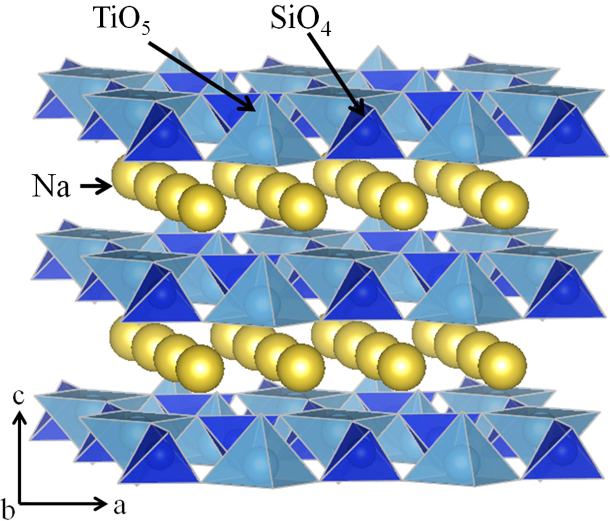
Considering this, we have focused on Na2TiSiO5 as Ti4+ contained white emission phosphor, because the Na2TiSiO5 consist TiO5 square pyramids in the crystal structure and TiO5 pyramidal shared corners with the SiO4 tetrahedral, which is separated by Na+ ions in the direction to the c axis (Fig. 1) [11, 22]. In addition, Na2TiSiO5 has high chemical and thermal stability, which is advantageous for obtaining phosphor particles of high crystallinity. It is previously reported that Na2TiSiO5 exhibits the bluish-white emission at low temperature (4.2 k). In this study, in order to further enhance the emission efficiency of the Na2TiSiO5 phosphor, Si4+ ions in the Na2TiSiO5 crystal lattice were partially substituted with Ge4+, because Na2TiGeO5 has similar crystal structure to that of Na2TiSiO5, which indicates that Ge4+ can be substituted in the Na2TiSiO5 lattice as solid solution form.
|
Fig. 1 Crystal structure of Na2TiSiO5. |
The crystal structure of the samples was identified through powder X-ray diffraction (XRD; Mac Science Ltd. MX-Labo) analysis. The emission and excitation spectra were measured at room temperature with a spectrofluorometer (Jasco Corp. FP-6500/6600), Where the emission spectrum was obtained for excitation at 254 nm and excitation spectrum was obtained for emission at 500 nm. The Commission International de I'Eclairage (CIE) chromaticity coordinate data for the samples were measured at room temperature with a luminescence colormeter (Hamamatsu C7473-36 PMA-11).
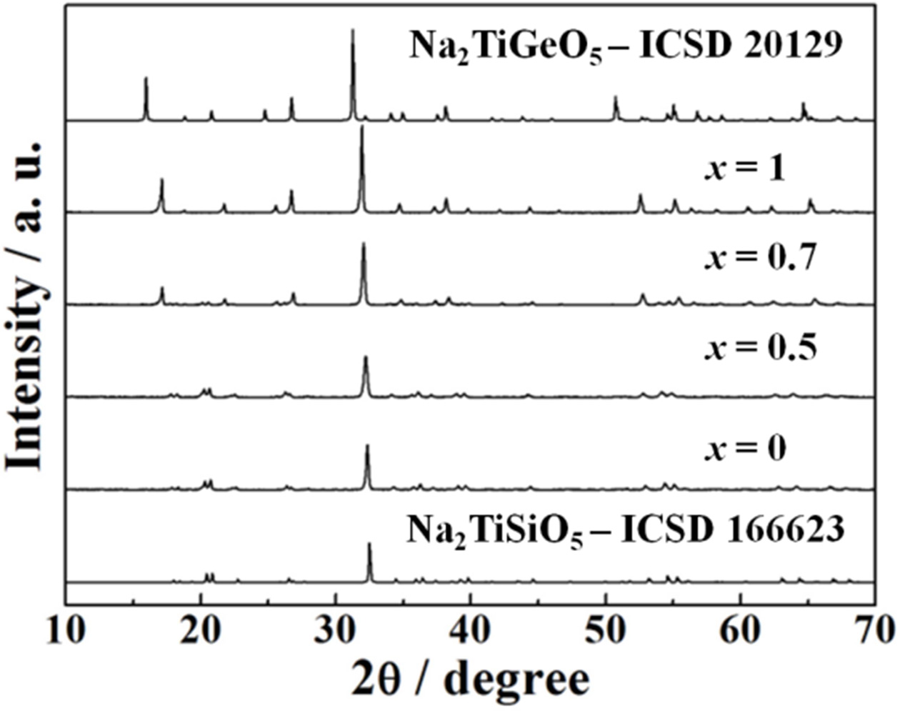
X-ray powder diffraction (XRD) patterns of the Na2TiSi1-xGexO5
(0 ≤ x ≤ 1.0) phosphors are shown in Fig. 2. The standard XRD patterns
of Na2TiSiO5 (#166623) and Na2TiGeO5
(#20129) from the inorganic crystal structure database (ICSD) are also shown in
Fig. 2 as a reference. The XRD patterns of the samples with x ≤ 0.5 were
identical to a single phase of highly crystalline orthorhombic Na2TiSiO5
structure. On the other hand, the crystal structure of the samples
transferred from Na2TiSiO5
to Na2TiGeO5 with increase in the Ge4+
content beyond x = 0.5 and these samples obtained in a single phase of
Na2TiGeO5. However, there are no diffraction peak
corresponding to any impurities in all XRD patterns, which is attributed to the
same crystal structure of both Na2TiSiO5 and Na2TiGeO5
[11,22]. In addition, a peak shift to a lower diffraction angle was
observed with increase in the Ge4+ content, because Si4+
(ionic radius: 0.026 nm for 4 coordination [23]) sites in the Na2TiSiO5
lattice is substituted with the larger Ge4+ (ionic radius: 0.026 nm
for 4 coordination [23]) to form solid solutions.
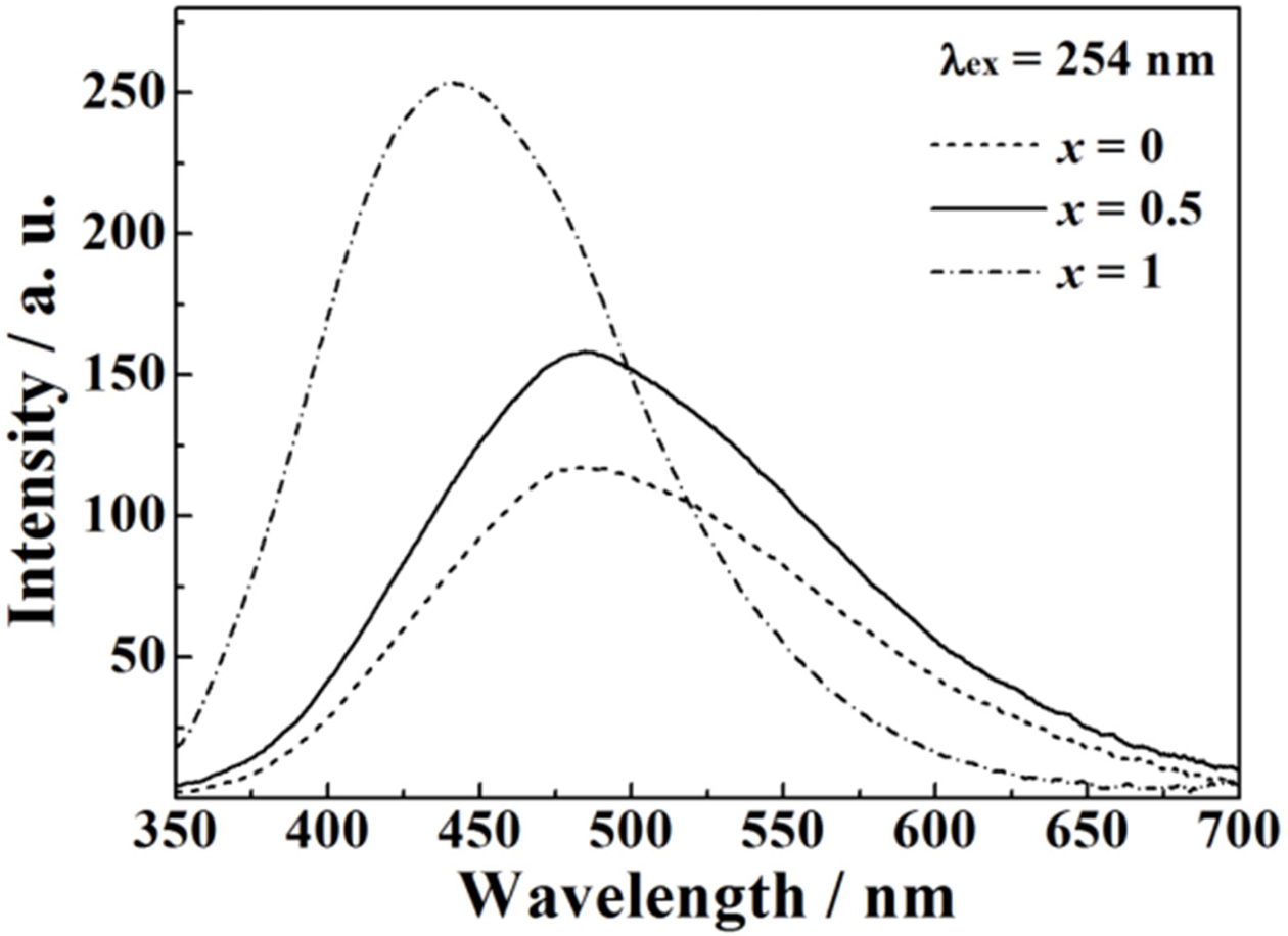
Fig. 3 shows the emission spectra of the Na2TiSi1-xGexO5
(0 ≤ x ≤ 1.0) phosphors with excitation at 254 nm. The emission spectra
of the samples with x ≤ 0.5 exhibit a broad bluish-white emission band
with a peak at 490 nm due to the charge transfer (CT) transition from 2p orbits
of O2− to 3d orbit of Ti4+, i.e., O2−-Ti4+
→ O−-Ti3+ in the isolated TiO5 polyhedron in
the Na2TiSiO5 lattices
[16, 17, 20]. The emission intensity of Na2TiSiO5
was effectively enhanced by the Ge4+ doping into
the crystal lattice, and the emission intensity of Na2TiSi0.5Ge0.5O5
was 1.35 times higher than that of Na2TiSiO5. In the
samples with x > 0.5, however, the emission band shifted to shorter
wavelength (higher energy) side with increase in the Ge4+
content, which is considered to be due to the phase
transition from Na2TiSiO5 to Na2TiGeO5.
The emission peak wavelength corresponding to charge-transfer (CT) transition
strongly depends on the excitation energy for the electron transfer between O2−
and Ti4+ in the crystal structure. Since the
electronegativity of Ge4+ (2.01 [24]) is higher than that
of Si4+ (1.90 [24]), the electronic attractive force between O2−
and Ti4+ in the Na2TiGeO5 is smaller than that
in the Na2TiSiO5, which leads to shift the emission band
to shorter wavelength (high energy) side due to increase the excitation energy
for the electron transfer from O2− to Ti4+ in the crystal
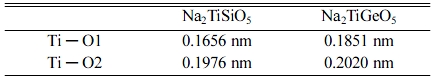
structure. In addition, the Ti4+-O2− bond length in the
Na2TiGeO5 lattice is larger than that in Na2TiSiO5
lattice (Table 1), which also leads to shift the emission band to shorter
wavelength side.
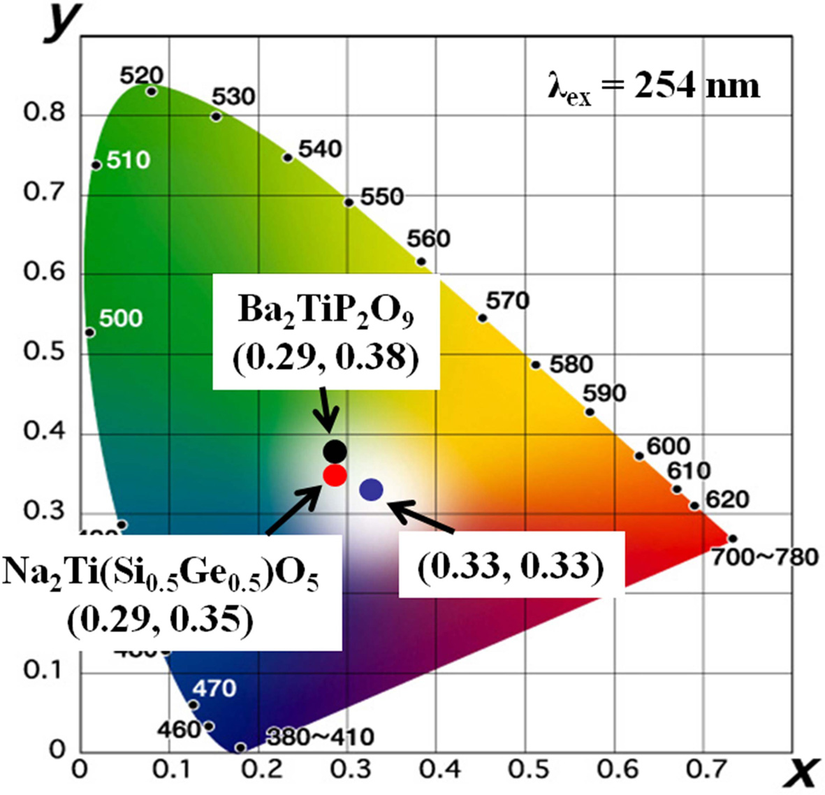
Fig. 4 presents the Commission International de
I'Eclairage (CIE) chromaticity diagram for the Na2TiSi0.5Ge0.5O5 phosphor. Results for a conventional Ti4+-contained
white emitting Ba2TiP2O9 phosphor is also
included for comparison. The CIE chromaticity coordinate values of the Na2TiSi0.5Ge0.5O5
phosphor were x = 0.29 and y = 0.35 under excitation at 254 nm UV
light, which is close to the standard white chromaticity (x = 0.33, y
= 0.33) for the NTSC system. In addition, the x and y values of
the Na2TiSi0.5Ge0.5O5 phosphor are
more close to white light compared with a conventional Ti4+
contained Ba2TiP2O9 phosphor (x = 0.29,
y = 0.38).
|
Fig. 2 XRD patterns of the Na2TiSi1-xGexO5 (0 ≤ x ≤ 1.0) phosphors. |
|
Fig. 3 Emission spectra of the Na2TiSi1-xGexO5 (0 ≤ x ≤ 1.0) phosphors under excitation at 254 nm. |
|
Fig. 4 CIE chromaticity diagram for the Na2TiSi0.5Ge0.5O5 and a conventional Ba2TiP2O7 phosphors. |
|
Table 1
|
Rare earth free white emitting Na2TiSi1−xGexO5 phosphors were in a single phase form synthesized by the conventional solid-state reaction method. These phosphors exhibited a broad bluish-white emission centered on 490 nm under excitation at 254 nm and the photoluminescence emission intensity was successfully enhanced by the Ge4+ doped into the Si4+ site in the Na2TiSiO5 lattice. The emission intensity of Na2TiSi0.5Ge0.5O5 was 1.35 times higher than that of Na2TiSiO5 and the CIE chromaticity coordinate values for the phosphor were x = 0.29 and y = 0.35 under excitation at 254 nm UV light.
This work was supported by a project from NEDO, New Energy and Industrial Technology Development Organization (Rare Metal Substitute Materials Development Project Development of Technology for Reducing Tb and Eu Usage in Phosphors for Fluorescent Lamp by High-speed Material Synthesis and Evaluation).
- 1. M.G. Brik, Y.X. Pan, and G.K. Liu, J. Alloys Compd. 509[5] (2011) 1452-1456.
-

- 2. T. Nishizaki and Y. Shimizu, J. Alloys Compd. 580 (2013) 369-372.
-
- 3. S.W. Kim, T. Hasegawa, H. Yumoto, T. Ishigaki, K. Uematsu, K. Toda, and M. Sato, J. Ceram. Process. Res. 15[3] (2014) 177-180.
- 4. V. Singh, G. Sivaramaiah, J.L. Rao, and S.H. Kim, Mater. Res. Bull. 60 (2014) 397-400.
-
- 5. X. Zhang, W. Jiang, Q. Pan, G. Yuan, and H.J. Seo, Mater. Lett. 128 (2014) 89-92.
-
- 6. G. Blasse and W.J. Schipper, Phys. Status Solidi A 25 (1974) K163-K165.
-
- 7. M.J. Treadaway and R.C. Powell, J. Chem. Phys. 61 (1974) 4003-4011.
-
- 8. R. Grasser and A. Scharmann, J. Lumin. 12-13 (1976) 473-478.
-
- 9. G. Blasse, Structure Bonding 42 (1980) 1-40.
- 10. P.F. Moulton, J. Opt. Soc. Am. B 3[1] (1986) 125-133.
-
- 11. B. Bouma and G. Blasse, J. Phys. Chem. Solids 56[2] (1995) 261-265.
-
- 12. G. Blasse, J. Lumin. 72-74 (1997) 129-134.
-
- 13. D. Kan, T. Terashima, R. Kanda, A. Masuno, K. Tanaka, S. Chu, H. Kan, A. Ishizumi, Y. Kanemitsu, Y. Shimakawa, and M. Takano, Nat. Mater. 4[11] (2005) 816-819.
-
- 14. Y. Takahashi, K. Kitamura, Y. Benino, T. Fujiwara, and T. Komatsu, Appl. Phys. Lett. 86[9] (2005) 091110.
-
- 15. A.J.H. Macke, J. Solid State Chem. 18[4] (1976) 337-346.
-
- 16. L.G.J. De Haart, A.J.De Vries, and G. Blasse, J. Solid State Chem. 59[3] (1985) 291-300.
-
- 17. M. Gaft, L. Nagli, G. Waychunas, and D. Weiss, Phys. Chem. Miner. 31[6] (2004) 365-373.
-
- 18. Y. Takahashi, K. Kitamura, N. Iyi, and S. Inoue, Appl. Phys. Lett. 88[15] (2006) 151903.
-
- 19. C. Moon, M. Nishi, K. Miura, and K. Hirao, J. Lumin. 129[8] (2009) 817-819.
-
- 20. A.J.H. Macke, J. Solid State Chem. 18[4] (1976) 337-346.
-
- 21. G. Blasse and G.J. Dirksen, Chem. Phys. Lett. 62[1] (1979) 19-20.
-
- 22. A. Waśkowska, L. Gerward, J. Staun Olsen, A. Sieradzki, and W. Morgenroth, J. Phys. Chem. Solids 69[4] (2008) 815-821.
-
- 23. R.D. Shannon, Acta Crystallogr., Sect. A 32[5] (1976) 751-767.
-
- 24. A.L. Allred, J. Inorg. Nucl. Chem. 17[3-4] (1961) 215-221.
-
 This Article
-
2019; 20(5): 460-463
Published on Oct 31, 2019
- 10.36410/jcpr.2019.20.5.460
- Received on Dec 10, 2018
- Revised on Jan 15, 2019
- Accepted on May 9, 2019
Services
- Abstract
introduction
experimental
results and discussion
conclusion
- Acknowledgements
- References
- Full Text PDF
Shared
Correspondence to
- Sun Woog Kim a, Kenji Toda b
-
aElectronic Convergence Materials Division, Optic & Display Materials Center, Korea Institute of Ceramic Engineering and Technology, Jinju, Korea
bGraduate School of Science and Technology, Niigata University, 8050 Ikarashi 2-nocho, Niigata 950-2181, Japan
Tel: +82-55-792-2487, Fax: +82-55-792-2492(Sun Woog Kim)
Tel: +81-25-262-6771, Fax: +81-25-262-6771(Kenji Toda) - E-mail: skim80@kicet.re.kr, ktoda@eng.niigata-u.ac.jp
Clean-Energy Research Institute(CRI), Hanyang University, 222, Wangsimni-ro, Seongdong-gu, Seoul, 04763, Korea
E-mail: jcpr@hanyang.ac.kr