


- Investigation of thermal annealing effects on the optical transparency and luminescent characteristics of Eu-doped Y2O3 thin films
Myun Hwa Chung and Joo Han Kim*
Department of Advanced Materials Engineering, Chungbuk National University, Cheongju 28644, Korea
The thermal annealing effects on the optical transparency and luminescent characteristics of the Eu-doped Y2O3 thin films have been investigated. The as-deposited Y2O3:Eu films exhibited an optical band gap of 5.78 eV with a transparency of 89 % at a wavelength of 550 nm. As the annealing temperature increased from 1000 to 1300 °C, the optical band gap and transparency of the films decreased from 5.77 to 4.91 eV and from 86.8 to 64.5 % at 550 nm, respectively. The crystalline quality of the films was improved with increasing annealing temperature. The annealed Y2O3:Eu films emitted a red-color photoluminescence (PL) with the highest emission peak near 612 nm. The PL intensity was increased with increasing annealing temperature to 1200 °C, resulting from the improvement in the crystalline quality of the films. The PL intensity was decreased with further increasing temperature above 1200 °C due to the formation of Y2SiO5 phase by the reaction of the film with the quartz substrate.
Keywords: Transparency, Optical band gap, Yttrium oxide, Thermal annealing
Lanthanide (Ln)-doped oxides are one of the most important
class of luminescent materials which have attracted intense attention. These
materials have been widely used in optical applications due to the unique
luminescent features of Ln ions [1-3] The light emission from the Ln ions
originates primarily from the 4fn intrashell transitions. The
partially filled 4f inner shell in the Ln ions is shielded from the
surroundings by the completely filled 5s2 and 5p6
outer shells. Therefore, the emission spectra of Ln ions generally appear as
very narrow and sharp peaks at wavelengths which are weakly dependent on the
coordination environment or the crystal field [3].
Among various Ln-doped oxides, europium-doped yttrium oxide (Y2O3:Eu) has been intensively studied owing to its red luminescence with high efficiency and good color purity [4-6]. Y2O3:Eu has been practically used as a red-emitting cathodoluminescent and photoluminescent material for various types of display devices, such as field emission displays (FEDs), vacuum fluorescent displays (VFDs), and plasma panel displays (PDPs) [7-10]. Y2O3:Eu is typically prepared in powdered form by using various synthesis techniques [4-12]. Special attention also needs to be paid to thin film form of Y2O3:Eu because it has diverse potential applications [13]. In particular, thin Y2O3:Eu films with a high transparency in the visible wavelength region could be used as a red light emission layer in transparent display devices [14]. In this study, optically transparent and luminescent thin films of Y2O3:Eu were deposited by radio frequency (RF) magnetron sputtering. This work primarily aimed to clarify the effects of thermal annealing treatment on the optical transparency and the luminescent characteristics of the Y2O3:Eu films. The relationship between the structure and luminescence of the Y2O3:Eu films was also examined.
The optically transparent Y2O3:Eu thin films were deposited by using an RF magnetron sputtering technique. Sputtering was carried out on fused quartz substrates using an Eu-doped Y2O3 target in an Ar gas atmosphere. Prior to deposition of the films, the sputtering chamber was pumped by a turbomolecular pump until a base pressure of less than 1 ´ 10-6 Torr was achieved. The deposition was performed with no substrate heating. The gas pressure and the RF power density were held at 2 ´ 10-2 Torr and 5.92 Wcm-2, respectively, during deposition. The film thickness was maintained at approximately 500 nm by adjusting the deposition time. The deposited films were thermally annealed for 1 hour in air ambient at temperatures from 1000 to 1300 °C.
The optical transmittance spectra of the Y2O3:Eu films were monitored on a Perkin Elmer Lambda 35 spectrophotometer in the spectral range between 190 and 1100 nm. The crystalline quality of the films was analyzed by X-ray diffraction (XRD), which was performed using a SmartLab Rigaku diffractometer equipped with Cu Kα1 radiation. To determine the surface morphology of the films, atomic force microscopy (AFM) measurements were performed using a Bruker Dimension Icon. Photoluminescence (PL) emission and excitation spectra of the films were measured at wavelengths from 200 to 800 nm with a resolution of 0.5 nm using a xenon discharge lamp as an excitation source.
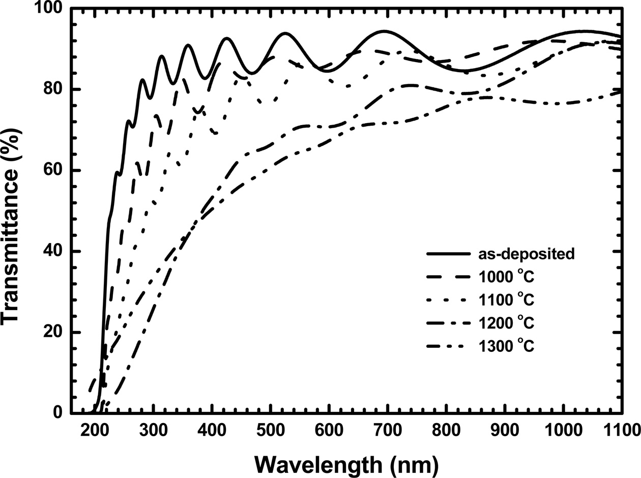
The optical transmission spectra were measured for
the Y2O3:Eu films and are presented in Fig. 1 with the variation of annealing
temperatures. The as-deposited films exhibit an optical absorption edge in
ultraviolet region and a high transparency in visible and near-infrared
regions. It can be seen that the transparency is reduced as the annealing
temperature increases. The as-deposited films have an optical transmittance of
89% at a wavelength of 550 nm. The transmittance reduces to 86.8% after
annealing the films at 1000 °C, and then to 64.5% after annealing at 1300 °C.
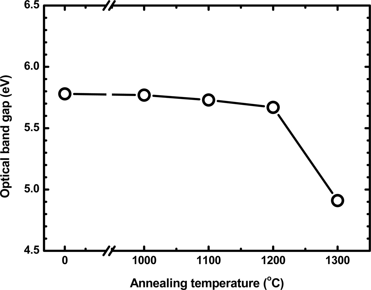
The optical band gap, Eg of the Y2O3:Eu films can be estimated using the
following equation [15]:
(α hn )2 = A(hn - Eg) (1)
where α is the optical absorption
coefficient, hν is the photon energy, and A is the constant. The obtained Eg
values are presented in Fig. 2 as a function of annealing
temperature. The Eg is found to be 5.78 eV for the as-deposited
films, which is comparable with the value reported for
yttrium oxide [16]. The Eg slightly decreases
as the annealing temperature increases to 1200 °C. A significant reduction
in Eg for the films annealed at 1300 °C is considered to be due
to the formation of Y2SiO5 phase, as will be discussed
below with the X-ray diffraction data.
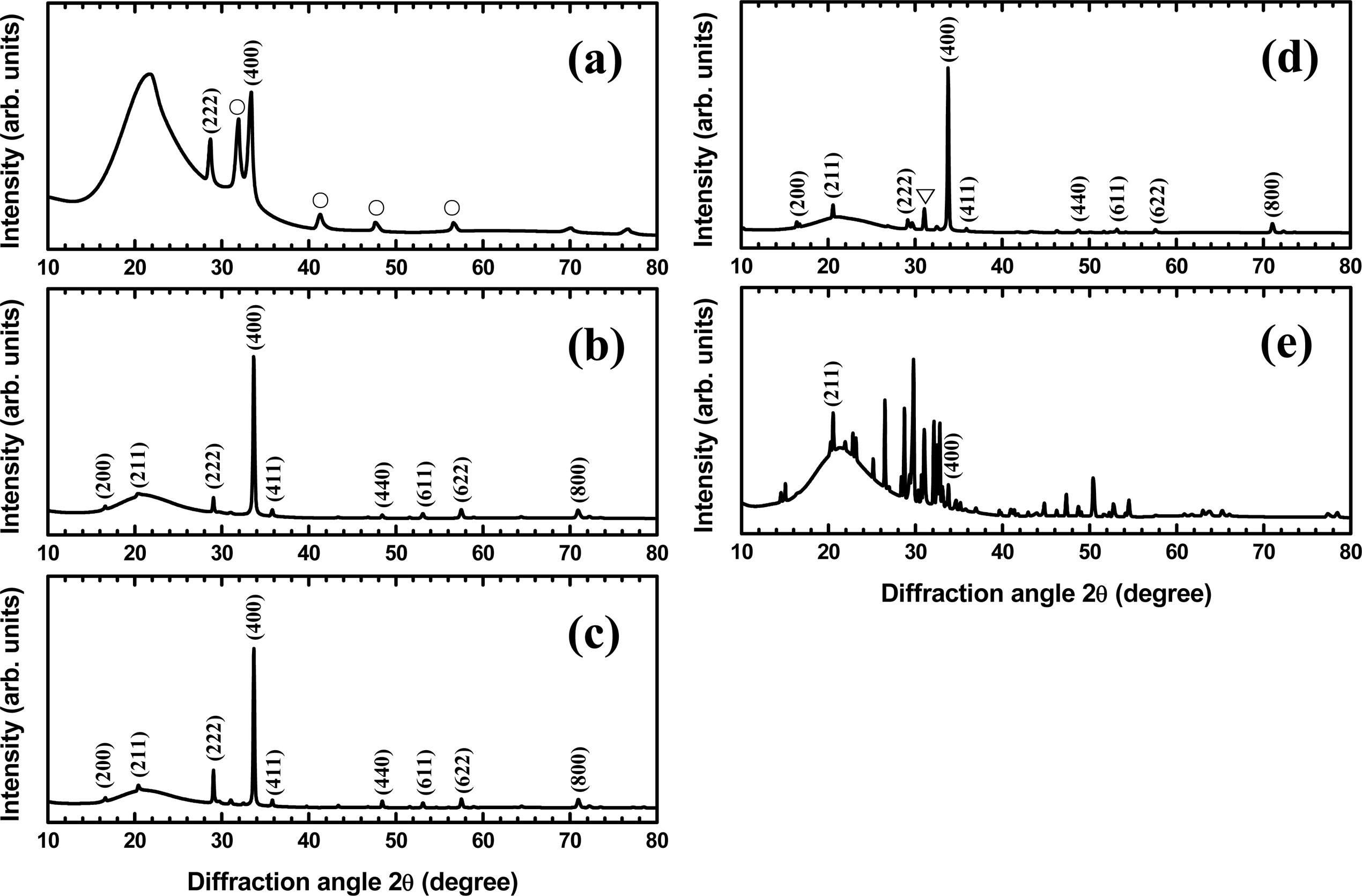
Fig. 3 presents the X-ray diffraction patterns of
the as-deposited Y2O3:Eu films and the films annealed at
different temperatures. It can be found in Fig. 3(a) that the as-deposited
films had a mixed structure of cubic and monoclinic Y2O3
phases. The peaks marked with Miller indices in the pattern are those from the
cubic Y2O3 phase [17]. The peaks
marked with the symbol (○) correspond to the monoclinic Y2O3 phase [18]. After
annealing treatment, the XRD patterns show much more intense and narrower peaks
as compared to those of the as-deposited films, indicating that the crystalline
quality of the films was significantly improved by the anneal. The annealed
films show the peaks from the cubic Y2O3 phase with a
preferential orientation along the (400) plane. After annealing at 1200 °C, as shown in Fig. 3(d), the diffraction peaks attributed to the Y2SiO5
phase start to appear. The peaks marked with the
symbol (5) correspond to the Y2SiO5
phase [19]. At 1300 °C, as shown in Fig. 3(e), the diffraction pattern is dominated by the peaks
from the Y2SiO5 phase as the reaction between the film
and the quartz substrate was accelerated at this high temperature. Most of the
peaks, except for the (211) and (400) peaks of the cubic Y2O3
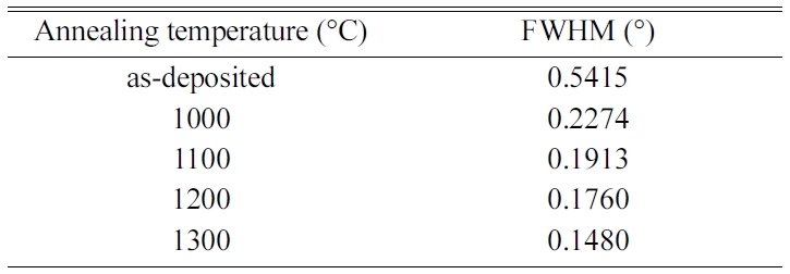
phase, arose from the Y2SiO5 phase. In order to analyze the crystalline quality of the films, we measured the full width at half maximum (FWHM) of the (400) peak from the cubic Y2O3
phase. As shown in Table 1, the FHWM is 0.5415° for the as-deposited films and significantly reduces to 0.2274° by annealing at 1000 °C. The FWHM decreases
with further increasing annealing temperature and reaches 0.1480 at 1300 °C. This clearly indicates the improved crystalline quality at higher
annealing temperature.
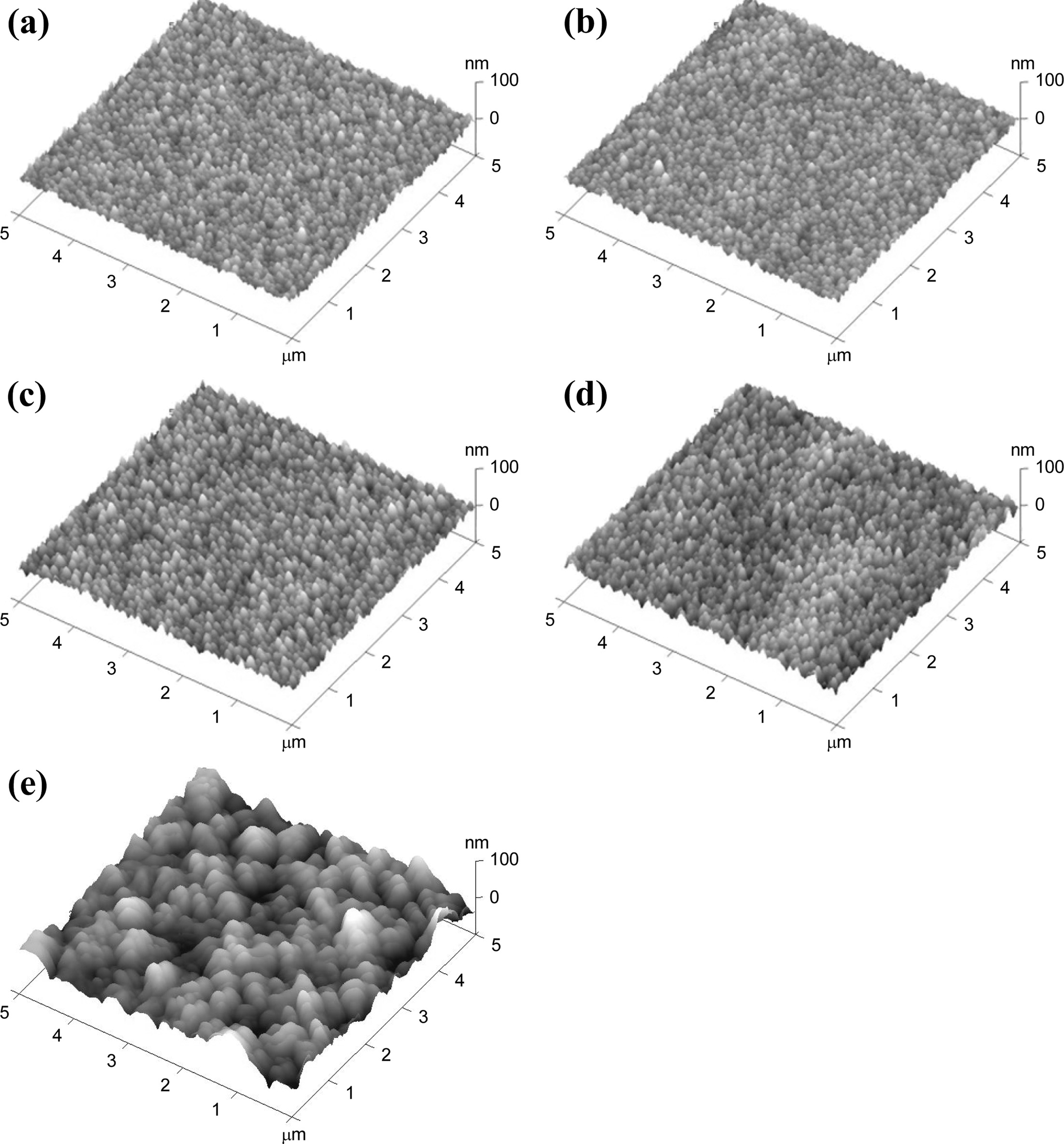
Fig. 4 shows AFM images for the as-deposited and annealed
Y2O3:Eu films. It can be found that no obvious change in
surface morphology was observed after annealing at temperatures up to 1100 °C. The surface of the films became rougher as the
annealing temperature was raised above 1200 °C,
resulting from the reaction between the film and the quartz substrate. It
should be mentioned that cracks appeared at the surface of the samples after
the annealing treatment. It is believed that the cracks were caused during
annealing, probably due to the difference of the thermal expansion coefficient
between the Y2O3:Eu film and the quartz substrate.
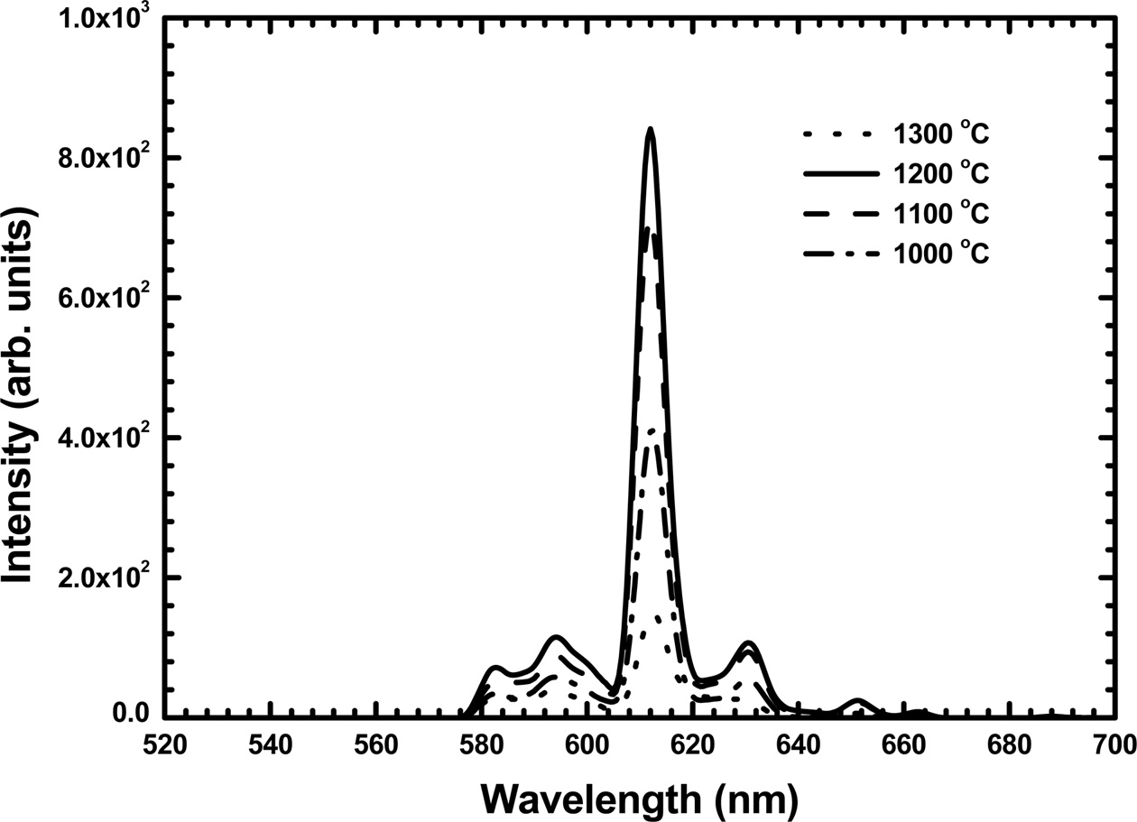
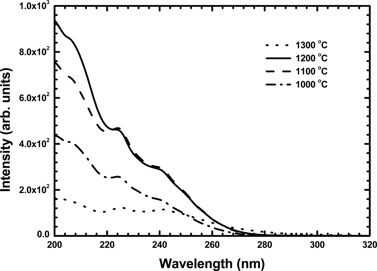
Fig. 5 shows the PL emission spectra of the Y2O3:Eu films annealed at different temperatures. The as-deposited films did not show any PL emission because of their poor crystalline quality. As shown in Fig. 5, several PL emission peaks were detected from the annealed films, which originated from the f – f transitions of Eu3+ ions. These PL spectra are similar to those observed from the Y2O3:Eu powders [8]. The highest emission peak near 612 nm in the red range is associated with the transition from the 5D0 excited state to the 7F2 level. The PL excitation spectra of the Y2O3:Eu films annealed at different temperatures are shown in Fig. 6. The excitation band below 219 nm is due to the absorption of Y2O3 host lattice. Additional bands observed in the range between 219 and 290 nm are related to the charge transfer between O2- and Eu3+ ions [3]. As the annealing temperature increased, the PL emission and excitation intensity increased and showed a maximum at 1200 °C. This was attributed to the improvement in the crystalline quality of the films. The PL emission and excitation intensity decreased at 1300 °C which was due to the formation of Y2SiO5 phase by the reaction of the film with the quartz substrate.
|
Fig. 1 The optical transmittance spectra obtained from the as-deposited Y2O3:Eu films and the films annealed at different temperatures. |
|
Fig. 2 The optical band gap as a function of the annealing temperature. |
|
Fig. 3 XRD patterns of the Y2O3:Eu films (a) as-deposited and annealed at (b) 1000 °C, (c) 1100 °C, (d) 1200 °C, and (e) 1300 °C. |
|
Fig. 4 AFM images of the Y2O3:Eu films (a) as-deposited and annealed at (b) 1000 °C, (c) 1100 °C, (d) 1200 °C, and (e) 1300 °C. |
|
Fig. 5 Photoluminescence emission spectra of the Y2O3:Eu films annealed at different temperatures. |
|
Fig. 6 PL excitation spectra of the Y2O3:Eu films annealed at different temperatures. |
|
Table 1 Full width at half maximum of
the (400) peak measured at different annealing temperatures. |
Optically transparent Y2O3:Eu films were deposited on fused quartz substrates by RF magnetron sputtering. We have shown that the optical transparency, crystalline quality, and luminescent characteristics of the Y2O3:Eu films were strongly affected by the thermal annealing treatment. The as-deposited Y2O3:Eu films showed a transparency of 89% at 550 nm and an optical band gap of 5.78 eV. The transparency and optical band gap of the films were found to decrease with increasing annealing temperature. XRD analysis revealed that the crystalline quality of the films was significantly improved by the thermal annealing treatment. The annealed Y2O3:Eu films showed a PL emission with the highest emission peak near 612 nm. The PL intensity was increased with increasing annealing temperature due to the improvement in the crystalline quality of the films. The PL intensity decreased at 1300 °C resulting from the formation of Y2SiO5 phase.
This work was supported by the National Research Foundation of Korea (NRF) grant funded by the Korea government (MSIT) (No. 2019R1F1A1040480).
- 1. W.-B. Pei, Z.-Y. Jing, L.-T. Ren, Y. Wang, J. Wu, L. Huang, R. Lau, and W. Huang, Inorg. Chem. 57[17] (2018) 10511-10517.
-

- 2. J. Janek, M. Soltys, L. Zur, E. Pietrasik, J. Pisarska, W.A. Pisarski, Mater. Chem. Phys. 180 (2016) 237-243.
-
- 3. G. Blasse and B.C. Grabmaier, in “Luminescent Materials” (Springer-Verlag, Berlin, Heidelberg, 1994) p. 25.
- 4. L. Ji, N. Chen, G. Du, M. Yan, and W. Shi, Ceram. Inter. 40 (2014) 3117-3122.
-
- 5. W. Cheng, F. Rechberger, and M. Niederberger, ACS Nano 10[2] (2016) 2467-2475.
-
- 6. W. Liu, Y. Wang, M. Zhang, and Y. Zheng, Mater. Lett. 96 (2013) 42-44.
-
- 7. D. Den Engelsen, P. Harris, T. Ireland, R. Withnall, and J. Silver, ECS J. Solid State Sci. Technol. 2[9] (2013) R201-R207.
-
- 8. W. Chen, M. Zhou, Y. Liu, S. Fu, Y. Liu, Y. Wang, Z. Li, Y. Li, Y. Li, and L. Yu, J. Alloys Compd. 656 (2016) 764-770.
-
- 9. J.A. Nelson, E.L. Brant, and M.J. Wagner, Chem. Mater. 15[3] (2003) 688-693.
-
- 10. Y. Shimomura and N. Kijima, Electrochem. Solid-State Lett. 7[2] (2004) H1-H4.
-
- 11. S.T. Mukherjee, V. Sudarsan, P.U. Sastry, A.K. Patra, and A.K. Tyagi, J. Alloys Compd. 519 (2012) 9-14.
-
- 12. X. Hou, S. Zhou, Y. Li, and W. Li, J. Alloys Compd. 494 (2010) 382-385.
-
- 13. P. H. Holloway, T. A. Trottier, B. Abrams, C. Kondoleon, S. L. Jones, J. S. Sebastian, and W. J. Thomes, J. Vac. Sci. Technol. B 17[2] (1999) 758-764.
-
- 14. D. Ghosh, P. Ghosh, T. Noda, Y. Hayashi, and M. Tanemura, Phys. Status Solidi-R 7[12] (2013) 1080-1083.
-
- 15. J. Tauc, in “Amorphous and Liquid Semiconductors” (Plenum, New York, 1974) p.159.
-
- 16. T. Das, C. Mahata, S. Mallik, S. Varma, G. Sutradhar, P. K. Bose, and C. K. Maiti, J. Electrochem. Soc. 159[3] (2012) H323-H328.
-
- 17. Joint Committee on Powder Diffraction Standards (JCPDS), Powder Diffraction Files, Inorganic, No. 43-1036.
- 18. Joint Committee on Powder Diffraction Standards (JCPDS), Powder Diffraction Files, Inorganic, No. 47-1274.
- 19. Joint Committee on Powder Diffraction Standards (JCPDS), Powder Diffraction Files, Inorganic, No. 36-1476.
 This Article
-
2019; 20(4): 431-435
Published on Aug 31, 2019
- Received on Apr 30, 2019
- Revised on Jul 22, 2019
- Accepted on Jul 24, 2019
Services
- Abstract
introduction
experimental
results and discussion
conclusions
- Acknowledgements
- References
- Full Text PDF
Shared
Correspondence to
- Joo Han Kim
-
Department of Advanced Materials Engineering, Chungbuk National University, Cheongju 28644, Korea
Tel : +82-43-261-2413
Fax: +82-43-271-3222 - E-mail: joohan@cbnu.ac.kr
Clean-Energy Research Institute(CRI), Hanyang University, 222, Wangsimni-ro, Seongdong-gu, Seoul, 04763, Korea
E-mail: jcpr@hanyang.ac.kr