


- Structural and electrical properties of (Ba0.7Sr0.3)TiO3 thin films for the application of electro-caloric devices
Min-Su Kwona, Sung-Gap Leea,*, Kyeong-Min Kima and Seungkeun Choib
aDept. of Materials Engineering and Convergence Technology, RIGET, Gyeongsang National University, Jinju 52828, Korea
bSchool of Science, Technology, Engineering & Mathmatics, UW, Bothell, WA 98011 USA
This study was conducted on the structural and electrical properties of (Ba0.7Sr0.3)TiO3 thin films prepared by the sol-gel and spin-coating methods in order to investigate their applicability to electrocaloric devices. All specimens showed a tetragonal crystal structure and lattice constants of a = 3.972 Å, c = 3.970 Å. The mean grain size of specimens sintered at 800 °C was about 30 nm, and the average thickness of 5 times coated specimens was 304~311 nm. In the specimen sintered at 750 °C, The relative dielectric constant and loss of specimens measured at 20 °C were 230 and 0.130, respectively, while dependence of the dielectric constant on unit DC voltage was -8.163 %/V. The remanent polarization and coercive fields were 95.5 μC/cm2 and 161.3 kV/cm at 21 °C, respectively. And, the highest electrocaloric property of 2.69 °C was observed when the electric field of 330 kV/cm was applied.
Keywords: (Ba,Sr)TiO3 thin films, sol-gel method, electro-caloric effect, ferroelectric, remanent polarization, dielectric constant
As electronic devices become more sophisticated and multifunctional, miniaturization of their size is rapidly advancing. Consequently, heat generation from these devices and substrates is becoming an important issue, and the electrocaloric (EC) effect emerged to overcome it. The EC effect means an adiabatic and reversible temperature change that occurs in a polar material upon application of an electric field [1]. Recently, the EC effects using various ferroelectric materials have been studied [2-5] and among them, the greatest temperature change (∆T = ~12K) of Pb(Zr0.95Ti0.05)O3 thin film to cooling devices have been reported [6]. However, PZT materials are limited in practical use due to environmental problems of the Pb elements and high curie temperature, despite their excellent EC characteristics.
The BaTiO3 ceramics, one of lead-free ferroelectric materials, exhibits various electrical characteristics such as dielectric, piezoelectric, and pyroelectric dispositions according to manufacturing conditions. And, these characteristics of the BaTiO3 ceramics are used for many applications such as capacitors, piezo-transducers. and infrared sensors [7, 8]. To improve the structural and electrical properties of BaTiO3 ceramics with a crystal structure of ABO3 perovskite, additions of impurities such as Ca, Pb, and Bi in the A-site as well as Zr, Sn, and Nb in the B-site have been studied [9, 10]. Especially, the (Ba1-xSrx)TiO3 (BST) ceramics has been studied for its applicability to microwave devices by using properties that can control phase transition temperatures according to Sr composition ratios [11-14]. There are a few studies of the EC effect of the BST bulk ceramics, but there are few studies of thin films [15, 16].
In this study, in order to investigate the BST films’ applicability to EC devices, the (Ba0.7Sr0.3)TiO3 composition was selected to obtain excellent dielectric properties at a phase transition temperature near room temperature. The BST thin films were prepared by the sol-gel and spin coating methods, which have the advantages of large area deposition with thickness uniformity, a precise stoichiometry control, relatively low temperature process and simple equipment. After that, structural and electrical properties of the BST films were measured.
This study selected the composition of (Ba0.7Sr0.3)TiO3 at a phase transition temperature near room temperature [13], which exhibited good dielectric properties based on temperature changes. And then, the thin films were fabricated by changing sintering temperatures. This was done by using the sol-gel and spin coating methods, since these methods allowed easier control of stoichiometric composition without a high production cost. BST precursor solutions were prepared by the sol-gel method from barium acetate (Junsei Chemical Co., Japan, 99.0%), strontium acetate 0.5-water (KANTO Chemical Co., Japan, 99.0%), titanium(IV) iso-propoxide (Junsei Chemical Co., Japan, 99.0%), as starting materials, with acetic acid and 2-methoxyethanol as solvents. The BST solution was passed through a syringe filter; then it was spin-coated onto Pt (100 nm)/Ti(10 nm)/SiO2 (100 nm)/p-Si (100) substrates using a spin coater operated at 3000 rpm for 25 s, followed by a drying step at 200 ℃ for 20 min in air to form gel films and a conducting pyrolysis step at 400 ℃ for 20 min to remove the organic materials, and finally annealed in the range 650-800 ℃ by using the rapid thermal annealing process. The crystalline structure of the BST thin films was analyzed via X-ray diffraction (XRD), and the surface and cross-sectional morphologies of the films were examined using scanning electron microscopy (SEM). For ferroelectric property measurements, Pt films were DC sputter-deposited onto the BST films as the top electrode with a diameter of 500 μm. The P-E hysteresis loops were analyzed using a ferroelectric test system (RT66B; Radiant Technologies Inc., Albuquerque, NM, USA).
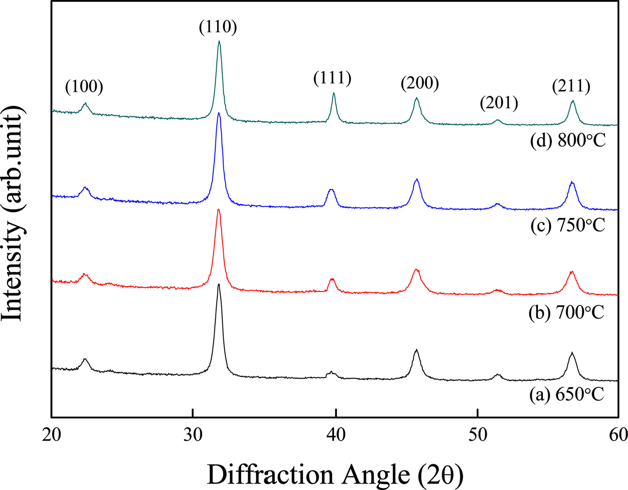
Fig. 1 shows the X-ray diffraction (XRD) patterns according to sintering temperatures of the BST thin film. At the sintering temperatures ranging from 650 °C to 800 °C, no XRD pattern of the second materials, like a pyrochlore phase, was observed. Although all specimens showed a tetragonal crystal structure, no dependence on sintering temperature occurred. The lattice constants were a = 3.972 Å, c = 3.970 Å, and they were smaller than those of the bulk specimen (a = 3.97~4.00 Å) [17]. This could have been caused by stress at the interfaces of the lower substrates during the crystallization process.
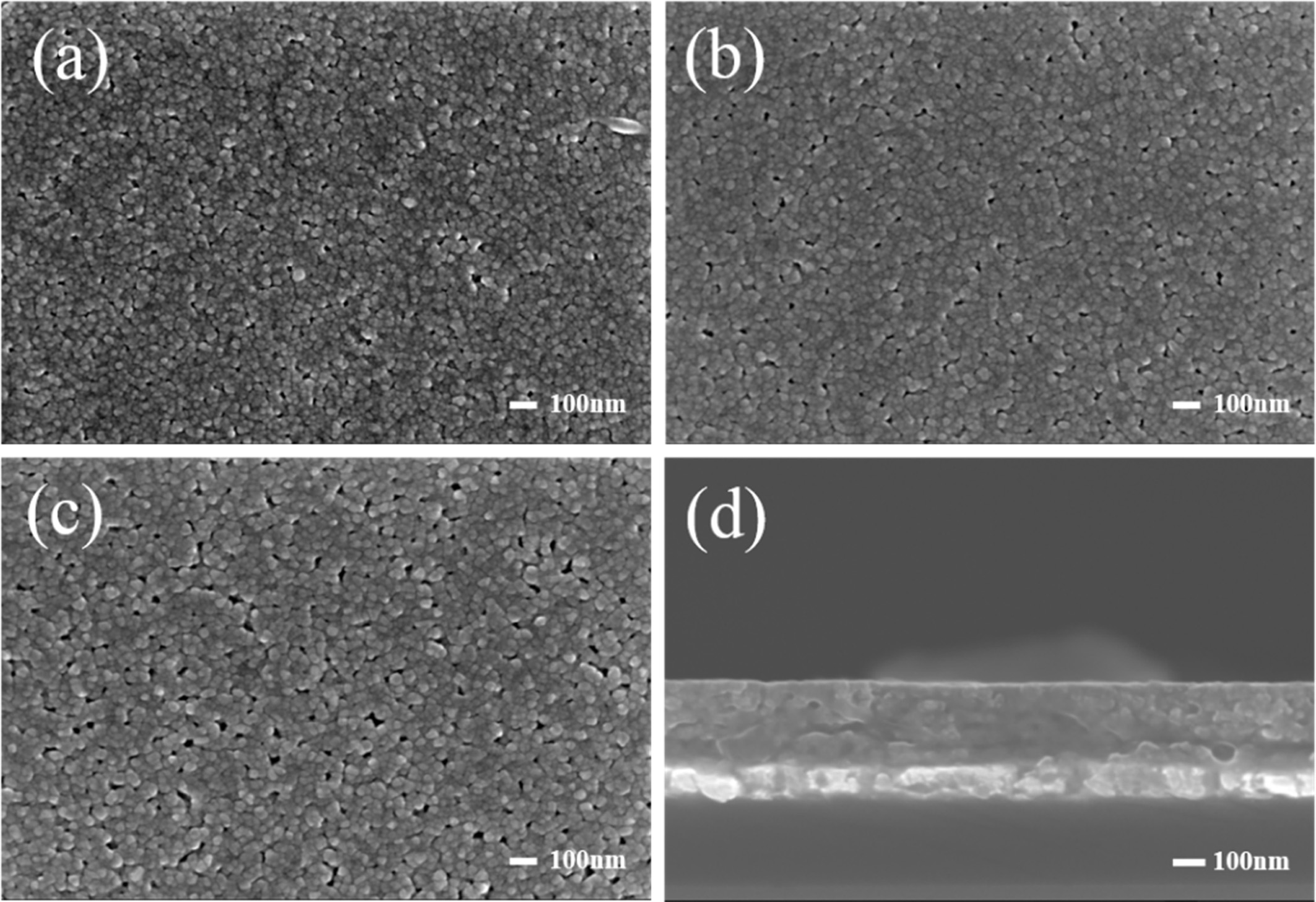
Fig. 2 shows the surface and cross-sectional microstructure of BST thin films with the variation of sintering temperatures. As a sintering temperature increased, the average grain size also increased. At the same time, the films showed a small and uniform grain distribution as well as a flat and compact cross-sectional structure. However, the specimen sintered at 800 °C showed an increase in pore distribution. The average grain size and thickness of BST thin film sintered at 750 °C were about 30 nm and 305 nm, respectively.
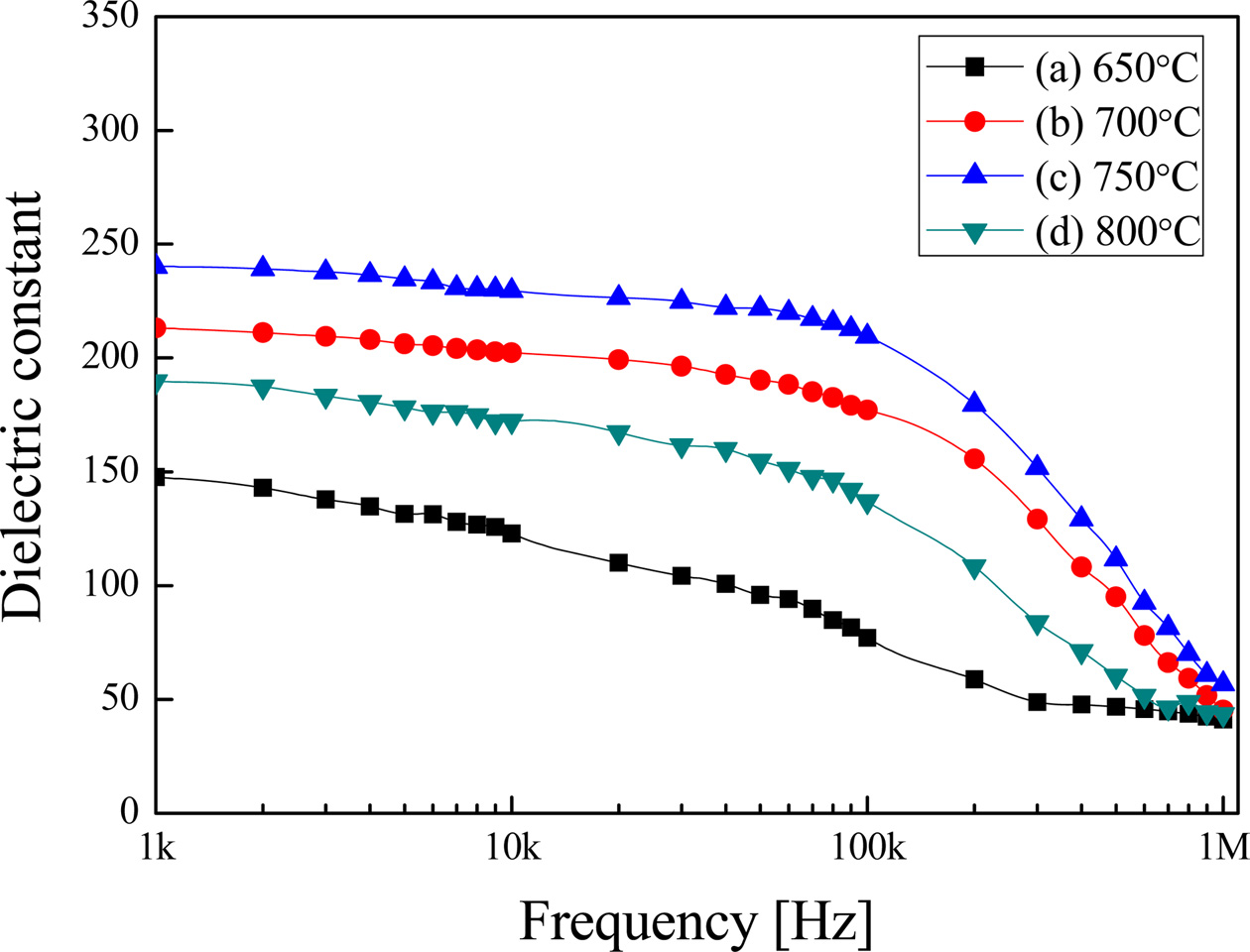
Fig. 3 shows the relative dielectric constant with the variation of applied frequency of BST thin films. It shows a typical characteristic of dielectric relaxation [18] in which the dielectric constant decreases when the applied frequency increases. As shown in Fig. 3, the BST thin film sintered at 750 °C showed the highest relative dielectric constant. The decrease of the relative dielectric constant at a frequency around 200 kHz could have been caused by suppressed polarization of space charge inside the specimen [19]. The specimens sintered at 800°C showed the largest average grain size, while the dielectric constant decreased as the pore distribution increased.
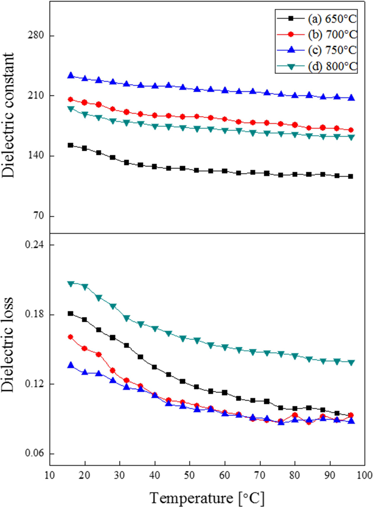
Fig. 4 shows the relative dielectric constant and loss of BST thin films by temperature. The relative dielectric constant decreased when the temperature was raised. This could be attributed to the fact that the phase transition temperature was lower than the measurement temperature’s range of 10~90 °C. Also, it could be attributed to increase in disorder of dipole arrangement due to characteristics of thermal energy and diffused phase transition. The dielectric constant and loss at 20 °C of the specimens sintered at 750 °C were 230 and 0.13, respectively.
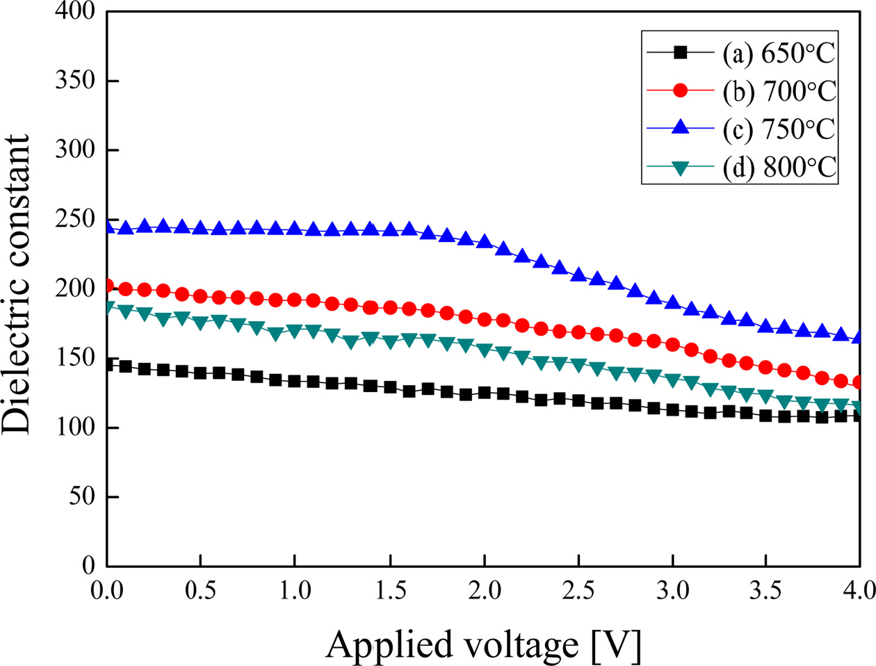
Fig. 5 shows the relative dielectric constant of BST thin films by applied DC voltage. The relative dielectric constant decreased when the applied DC voltage was raised. This is due to a clamping effect of suppressing the rotation and displacement of dipoles by an externally applied DC electric field. When a DC voltage was applied to the BST thin films sintered at 750 °C, the relative dielectric constant decreased at a slope of -8.163 %/V.
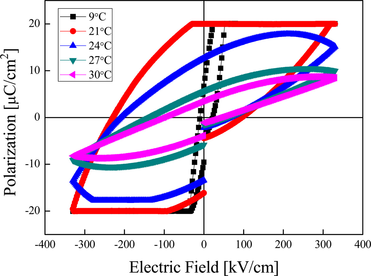
Fig. 6 shows the hysteresis loops of BST thin films sintered at a temperature of 750 °C. When the temperature became higher, the polarizations and coercive fields decreased due to increase in disorder of dipoles inside the crystal. The polarization and coercive field at 21 °C exhibited excellent properties of 95.5 μC/cm2 and 161.3 kV/cm, respectively. In a case of specimens sintered at 800 °C (not shown in this paper), the polarization decreased due to presence of pores. As shown in Fig. 4, the phase transition of the BST thin film was distributed at a temperature below 10 °C. And, the phases of ferroelectric and transition coexisted due to characteristics of diffused phase transition. Therefore, the polarization and coercive field properties exhibited at about 20 °C due to polarization induced by the applied electric field in measurement of hysteresis curve.
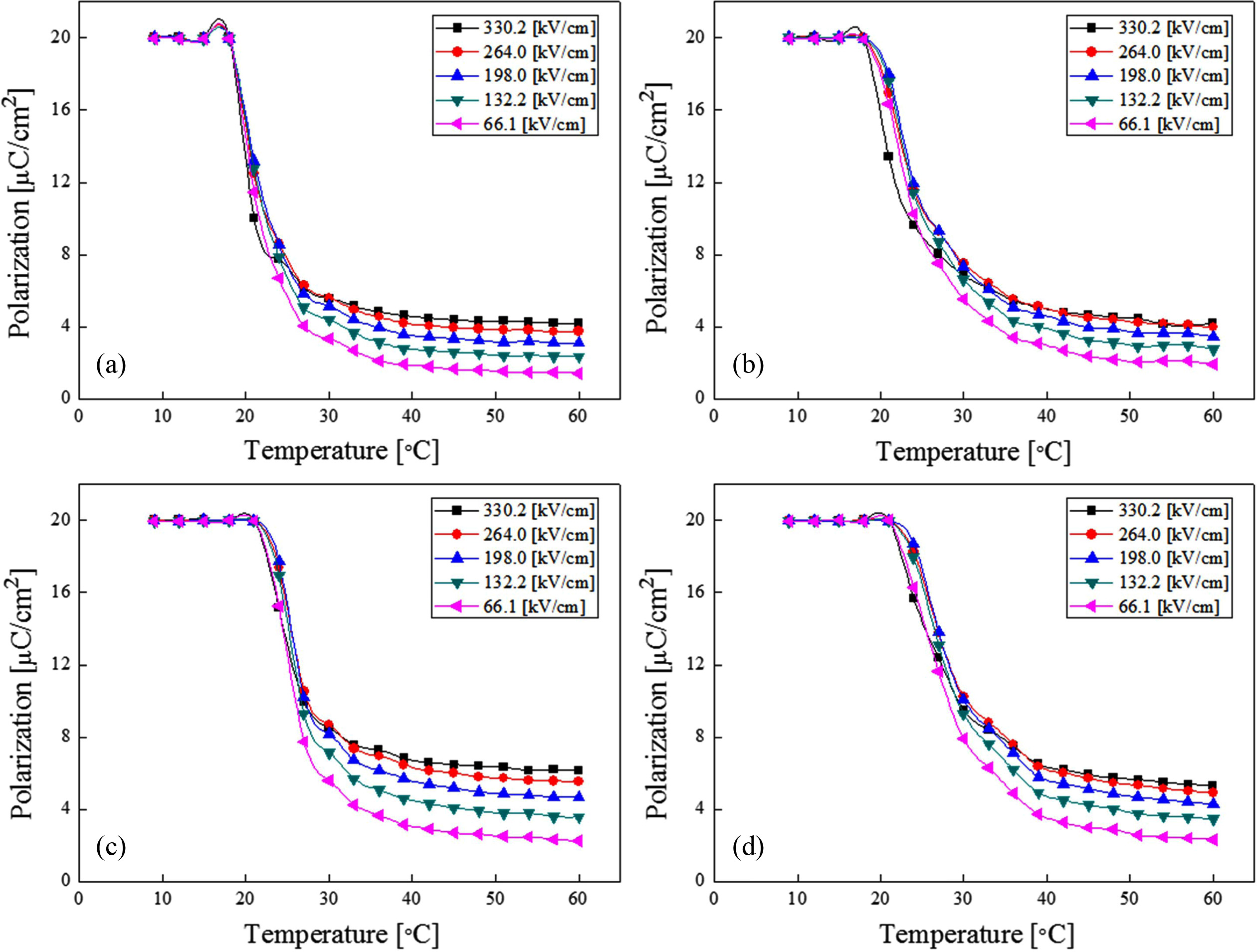
Fig. 7 shows the polarization of BST thin films by temperature change and applied electric field. While the maximum polarization of each thin film was fixed at 20 μC/cm2, the relative reduction properties by temperature change were shown. The remanent polarization could have rapidly decreased to a degree between 20 and 25 °C due to its critical temperature. At this temperature, the disorder of dipole array rapidly increased as the temperature in the vicinity of the phase transition region also increased. Also, the polarization increased when the applied DC field was raised. This is because the disorder of dipole distribution by thermal energy exhibited the field-induced ferroelectric state, as it was rearranged by the externally applied DC electric field.
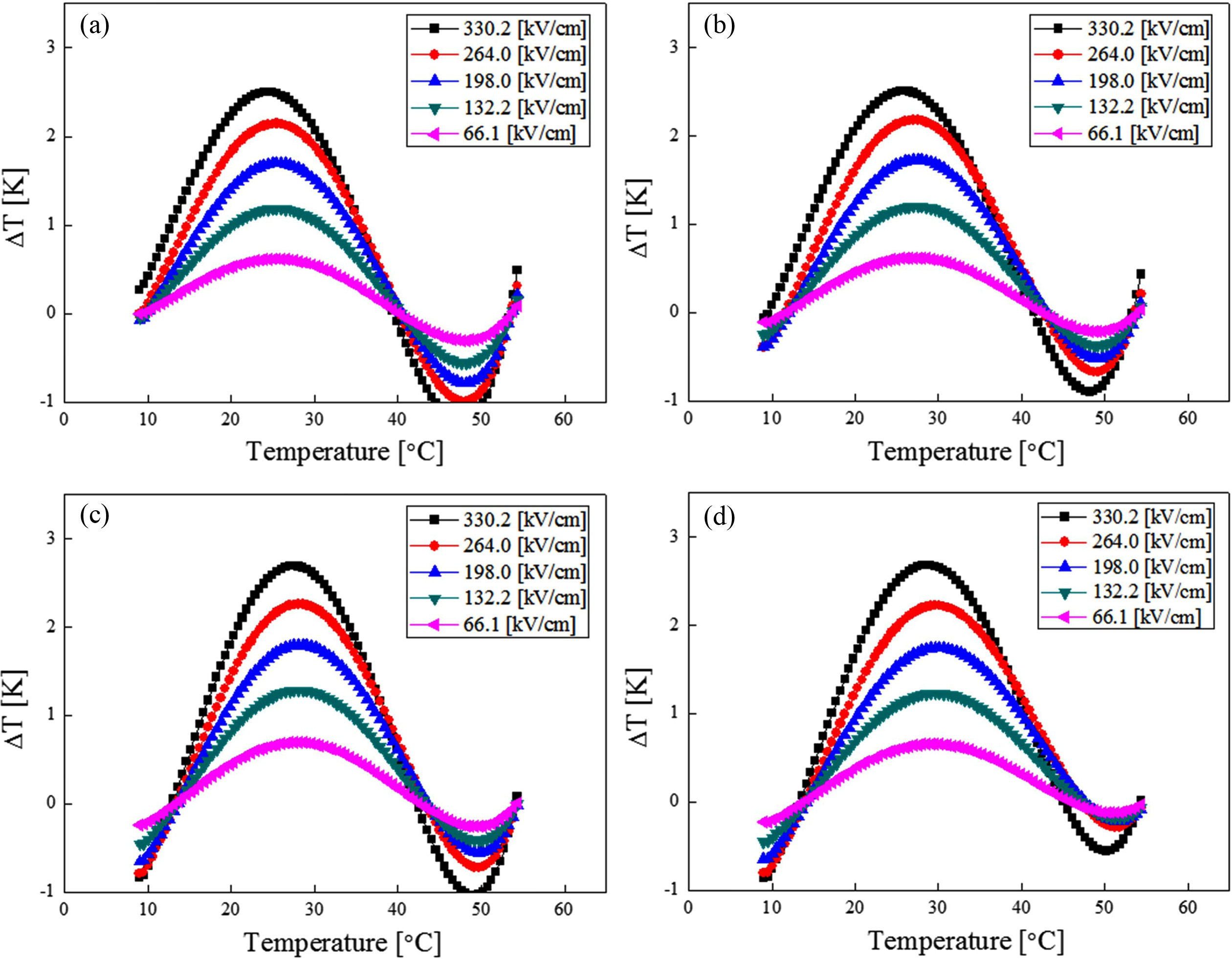
Fig. 8 shows the EC properties (ΔT) of BST thin films by temperature change. When the electric field of 330 kV/cm was applied to the thin films sintered at 750 °C, the highest EC property of 2.69 °C was shown at around 30 °C. All specimens exhibited excellent EC properties at a temperature little higher than the Curie temperature. This could have been caused by the EC properties that were maximized close to a certain temperature. At this temperature, the dependency of the dipole rearranged by the electrical field became maximum due to coexistence of the ferroelectric and paraelectric phases.
|
Fig. 1 X-ray diffraction patterns of (Ba0.7Sr0.3)TiO3 thin films with the variation of sintering temperature. |
|
Fig. 2 Surface and cross-sectional microstructure of (Ba0.7Sr0.3)TiO3 thin films with the variation of sintering temperature; (a) Surface, 700 ℃, (b) Surface, 750 ℃, (c) Surface, 800 ℃, and (d) Cross-section, 750 ℃. |
|
Fig. 3 Relative dielectric constant of (Ba0.7Sr0.3)TiO3 thin films with the variation of the applied frequency. |
|
Fig. 4 Relative dielectric constant and dielectric loss of (Ba0.7Sr0.3)TiO3 thin film with the variation of temperature change. |
|
Fig. 5 Fig. 5. Relative dielectric constant of (Ba0.7Sr0.3)TiO3 thin film with the variation of DC voltage applied. |
|
Fig. 6 Hysteresis loops of (Ba0.7Sr0.3)TiO3 thin films sintered at 750 ℃ with the variation of temperature change. |
|
Fig. 7 Polarization of (Ba0.7Sr0.3)TiO3 thin film with temperature change and applied electric field; (a) 700 ℃, (b) 750 ℃, (c) 800 ℃ and (d) 850 ℃. |
|
Fig. 8 Electro-caloric properties (ΔT) of (Ba0.7Sr0.3)TiO3 thin film with temperature change; (a) 700 ℃, (b) 750 ℃, (c) 800 ℃ and (d) 850 ℃. |
This study was conducted on the structural and electrical properties of thin (Ba0.7Sr0.3)TiO3 films prepared by the sol-gel method in order to investigate the films’ applicability to operating EC devices at room temperature. The specimens sintered at temperatures between 650 °C and 800 °C showed a tetragonal crystal structure. Also, neither a secondary phase nor unreacted material was observed. The average grain size increased when the sintering temperature was raised. At the same time, a flat and dense cross-sectional structure was obtained. The relative dielectric constant decreased when the applied frequency was increased. The decrease of the dielectric constant at a frequency of 200 kHz or higher could have been caused by decrease in polarization of internal space charge. The EC effect showed the highest value at a temperature slightly higher than the Curie temperature, while the ferroelectric and paraelectric phases coexisted.
This work was supported by Basic Science Research Program through the National Research Foundation of Korea (NRF) funded by the Ministry of Education (No. 2017R1D1A3 B03032164) and by the Gyeongsang National University Fund for Professors on Sabbatical Leave, 2018.
- 1. A.L. Moore, L. Shi, Mater. Today 17 (2014) 163-174.
-

- 2. X. Yan, M. Zhu, Q. Wei, S.-G. Lu, M. Zheng and Y. Hou, Scripta Materialia 162 (2019) 256-260.
-
- 3. Z. Jiang, G.-P. Zheng and S. Ullah, Ceramics International 45 (2018) 2876-2880.
-
- 4. Y. Liu, J. F. Scott and B. Dkhil, Appl. Phys. Rev. 3 (2016) 031102.
-
- 5. R. Pirc, Z. Kutnjak, R. Blinc, and Q. M. Zhang, J. Appl. Phys. 110 (2011) 074113.
-
- 6. T. Zhang, W. Li, W. Cao, Y. Hou and W. Fei, Appl. Phys. Lett. 108 (2016) 162902.
-
- 7. H. Kishi, Y. Mizuno and H. Chazono, Jpn. J. Appl. Phys. 42 (2003) 1-15.
-
- 8. A.S. Bhalla, R. Guo and R. Roy, Mat. Res. Innovat. 4 (2000) 3-26.
-
- 9. Han. Y. H, J.B. Appleby and D.M. Smyth, J. Am. Ceram. Soc. 70 (2003) 96-100.
-
- 10. B. Garbarz-Glos, K. Bormanis and D. Sitko, Mat. Res. Ferroelectrics, 417 (2011) 118-123.
-
- 11. B. Su, J.E. Holmes, C. Meggs and T.W. Button, J. Eur. Ceram. Soc. 23 (2003) 2699-2703.
-
- 12. M. Noda, T. Yamada, K. Seki, T. Kamo, K. Yamashita, H. Funakubo and M. Okuyama, IEEE Trans. Ultrason. Ferroelectr. Freq. Control 57 (2010) 2221.
-
- 13. A. Ghandouria, S. Sayouria, T. Lamcharfi, L. Hajji, J. Ceram. Process. Res. 19[3] (2018) 154-170.
- 14. K. J. Lee, C. H. Lee, S. K. Jung, G. H. Lee, W. S. Cho and W. S. Hwang, J. Ceram. Process. Res. 18[1] (2017) 45-50.
- 15. Z. Xu, H. Qiang, Materials Letters 191 (2017) 57-60.
-
- 16. X. Liu, T. Chen, M. Fu, Y. Wu, X. Chen, Ceramic International 40 (2014) 11269-11276.
-
- 17. H. HE, W. Cai, R. Gao, G. Chen, X. Deng and C. Fu, Advanced Funtional Materials (2011) 587-598.
-
- 18. S.Y. Wang, B.L. Cheng, Can Wang, W. Peng, S.Y. Dai, Z.H. Chen, Key Engineering Materials 280-283 (2005) 81-84.
-
- 19. S. Dash, R.N.P. Choudhary, P.R. Das and A. Kumar, Can. J. Phys. 93 (2015) 738-744.
-
 This Article
-
2019; 20(4): 395-400
Published on Aug 31, 2019
- Received on Mar 15, 2019
- Revised on Jul 5, 2019
- Accepted on Jul 5, 2019
Services
- Abstract
introduction
experimental
results and discussion
conclusions
- Acknowledgements
- References
- Full Text PDF
Shared
Correspondence to
- Sung-Gap Lee
-
Dept. of Materials Engineering and Convergence Technology, RIGET, Gyeongsang National University, Jinju 52828, Korea
Tel : +82-55-772-1687 - E-mail: lsgap@gnu.ac.kr
Clean-Energy Research Institute(CRI), Hanyang University, 222, Wangsimni-ro, Seongdong-gu, Seoul, 04763, Korea
E-mail: jcpr@hanyang.ac.kr